 50.002 CS
- Using Verilog with Alchitry Labs
- Installation
- Module (Verilog)
- Net types and Variable types
- The
alwaysBlock - Simulation (Verilog + Icarus)
- Value assignment
- Inputs, interactivity, and bit-flow in Simulation
- Arrays in Verilog
- Putting it all together
- Auto truncation, auto extension, and width mismatches
- Other
alwaysforms (preview) - A Caveat: Evaluation Order
- Summary
- Epilogue: How are Modules Realised?
- From Simulation to Real Hardware
- Appendix
50.002 Computation Structures
Information Systems Technology and Design
Singapore University of Technology and Design
(Verilog) Lab 1: Digital Abstraction with Hardware Design Language
This is a Verilog parallel of the Lucid + Alchitry Labs Lab 1. It is not part of the syllabus, and it is written for interested students only.
We are using Verilog-2005 and not SystemVerilog for simplification and educational purposes. Verilog-2005 is a subset of SystemVerilog so it would still be compatible with SystemVerilog. Another major motivation is that Alchitry Labs also support Verilog interopability.
You add Verilog modules and instantiate them from Lucid, hence allowing you to easily integrate them into Lucid projects should some of your group members still prefer to work in Lucid.
If you are reading this document, we assume that you have already read Lab 1 Lucid version, as some generic details are not repeated (e.g: FPGA Toolchain used in 50.002, what FPGA is for, etc). This lab has the same objectives and related class materials so we will not paste them again here. For submission criteria, refer to the original lab 1 handout.
Using Verilog with Alchitry Labs
This alternate Verilog-track version exists for students who already have some prior exposure to HDL, or who want a closer look at what Lucid is ultimately translated into.
Alchitry Labs can create and edit Verilog modules, and Verilog can be part of an FPGA project. However, the convenient Alchitry Labs IO simulation panel (buttons, switches, LEDs, etc.) is intended for Lucid simulations, so your Verilog modules will not “show up” in that same interactive simulator view.
Therefore, in this lab, we will do simulation only using Icarus Verilog:
- write Verilog (
.v) modules and a testbench- compile with
iverilog- run with
vvp
Later, once you are comfortable reading and writing basic Verilog, we can return to Alchitry Labs and show how Verilog modules fit into the full FPGA toolchain (constraints, build, and hardware programming). We will only do this in Lab 4.
Analogy
A good analogy is learning programming with Python before C. Python helps you focus on core computational ideas without fighting low-level details on day one. C forces you to be explicit about more details and gives you more control, but also more ways to make mistakes. In the same way, Lucid is the “high-level on-ramp” for 50.002, while Verilog is a “closer-to-the-metal” view for those who are curious.
Choosing Lucid does not put you at a disadvantage for this course. The Verilog track is here primarily to satisfy advanced interest, not because Lucid is lacking.
Installation
For this introductory lab, you do not need Vivado (yet), and you do not need Alchitry Labs to transpile anything because we are not going to load the binary to the hardware yet. Instead, you will compile and run Verilog simulations locally using Icarus Verilog (iverilog + vvp).
What you need for now:
iverilog(compiler)vvp(simulation runtime)
After installing, confirm both commands work by running:
iverilog -V
vvp -V
If both print version information, your setup is done.


You can see the installation step-by-step in the appendix.
Files and folder layout
Create this structure:
lab1_verilog/
  src/
  test/
How to compile and run
From inside lab1_verilog/, compile the corresponding source file and testbench:
iverilog -g2005 -o lab1.vvp src/<FILENAME>.v test/<FILENAME>.v
vvp lab1.vvp
If compilation and run succeed, you should see printed output from the testbench.
-g2005 option enable syntax/features aligned with IEEE Verilog-2005 (often also labeled “Verilog 2005”).
Module (Verilog)
Modules are the core building blocks of any HDL project. They encapsulate specific functionality, allowing you to design complex circuits by breaking them into smaller, manageable components. Each module can have parameters and ports that define how it interacts with other parts of the design.
In Verilog, a module looks like this:
module module_name #(
  // optional parameter list
) (
  // port list
);

  // module body

endmodule
By organizing your design into modules, you create reusable, testable blocks that can be combined to form larger systems.
Here is one example:
    module invert8 (
        input  [7:0] a,
        output [7:0] y
    );
        assign y = ~a;
    endmodule
Port List
Each module should have a list of ports, which are like the input and output of a function. Ports are declared with input and output. In Verilog, you may also see a type written together with the port declaration, most commonly wire or reg. Read this section to find out the difference.
In port list declaration, inputs are wires entering the module, while outputs are also wires leaving the module.
Example (outputs driven by continuous assignments, so plain outputs are fine):
module example_block (
  input        a,         // 1-bit input wire
  input  [7:0] b,         // 8-bit input bus (8 wires)
  output       y,         // 1-bit output (driven by assign)
  output [7:0] z          // 8-bit output bus (driven by assign)
);
  assign y = a;
  assign z = b;
endmodule
Example (outputs driven by an always @* block, so they must be declared reg):
module example_block2 (
  input        a,
  input        b,
  output reg   y
);
  always @* begin
    y = a & b;
  end
endmodule
You can declare N bit ports using the [MAX:MIN] syntax. In the example above:
ais 1 wire (1 bit)b[7:0]is 8 wires bundled into one bus
Module Body
The module body defines connections and logic that exist in this module.
A typical module body contains:
- Internal signals (wires/regs) used to connect pieces inside the module
- Module instances (instantiations of other modules)
- Combinational logic (
always @*) and/or sequential logic (always @(posedge clk))
However, the most direct way to express pure combinational wiring is a continuous assignment with the assign keyword.
module invert8 (
  input  [7:0] a,
  output [7:0] y
);
  assign y = ~a;   // 8 NOT gates in parallel
endmodule
You use always @* when the combinational logic needs procedural structure or when you want a “default then override” pattern. For simple combinational expressions, assign is preferred and clearer.
module clamp1 (
  input  a,
  input  force_zero,
  output reg y
);
  always @* begin
    if (force_zero) y = 1'b0;
    else            y = a;
  end
endmodule
This is still purely combinational, but if needs an always @* block.
always Construct and Sensitivity Lists
The
alwaysblockIn Verilog, an
alwaysblock is a procedural region that re-evaluates whenever its event control triggers. For combinational modules, the intent is that the block re-runs whenever any input it depends on changes, so the output continuously reflects the current inputs (no state).
With an explicit sensitivity list, the designer enumerates which signals trigger re-evaluation. This is correct only if the list is complete.
// 2:1 MUX with an explicit sensitivity list (must be complete)
always @(a or b or sel) begin
  if (sel) y = b;
  else     y = a;
end
A common beginner error is omitting a read signal from the list. The code may still synthesize to the intended hardware, but simulation can become misleading because the block simply does not run when the omitted signal changes.
// Buggy for simulation: sel is read but not in the sensitivity list
always @(a or b) begin
  if (sel) y = b;
  else     y = a;
end
To avoid this class of errors, combinational logic is typically written with always @*, which instructs the simulator to make the block sensitive to all signals read within it.
// Recommended combinational style
always @* begin
  if (sel) y = b;
  else     y = a;
end
If you’d like to go into a deep dive about sensitivity lists, read this article.
Internal Signals (wire and reg)
Inside a module, you often need internal connections, which you can declare as wire or reg. Similar to port list:
wireis used for signals driven by continuous assignments (assign) or by outputs of other modulesregis used for signals assigned inside analwaysblock
Examples of internal declarations:
wire       x;       // 1-bit internal wire
wire [7:0] y;       // 8-bit internal bus

reg        s;       // 1-bit signal assigned in always
reg  [3:0] state;   // 4-bit signal assigned in always
Example usage for wire:
module wire_example (
  input  a,
  output y
);
  wire nota;
  assign nota = ~a;     // nota is driven by continuous assignment
  assign y    = nota;   // y is connected to nota
endmodule
Example usage for reg:
module reg_example (
  input  a,
  input  b,
  output y
);
  reg tmp;

  always @* begin
    tmp = a & b;        // tmp is assigned in an always block
  end

  assign y = tmp;
endmodule
Module Instances (Instantiation)
A module can use other modules by instantiating them. This is the heart of building bigger systems from smaller blocks.
Example: suppose you have a module child:
module child (
  input  a,
  output y
);
  assign y = ~a;
endmodule
You can instantiate it inside another module:
module parent (
  input  a,
  output y
);

  // internal wire to connect signals
  wire y_internal;

  // instantiate child
  child u1 (
    .a(a),
    .y(y_internal)
  );

  // connect internal wire to output
  assign y = y_internal;

endmodule
The syntax is simple:
<module_type> <instance_name>(.<port_name>(<value>),...)
In HDL, instantiation is like placing a component on a circuit: like when you want to build a computer and you “instantiate” (buy) a CPU, few RAM sticks, and GPU.
The port connections (the .a(a) and .y(y_internal)) are literally “wiring it up”
Named vs positional port connections
There are two ways to connect the ports. It is recommended to use the named connection:
child u1 (
  .a(a),
  .y(y_internal)
);
Positional assignment is allowed but really easy to mess up:
child u1 (a, y_internal);
Parameters
Parameters let you make modules configurable (for width, number of stages, etc.). However, we do not use it much here until the later labs.
Syntax:
module thing #(
  parameter WIDTH = 8
) (
  input  [WIDTH-1:0] a,
  output [WIDTH-1:0] y
);
  assign y = a;
endmodule
When instantiating:
thing #(.WIDTH(16)) u1 ( .a(a16), .y(y16) );
Net types and Variable types
In Verilog, signals fall into two broad categories:
Net types (wires)
A net represents a physical connection, like a wire on a schematic. Nets do not “store” values. They must be driven by something else.
Common net type:
wire(the one you will use almost all the time in this lab)
A net is driven by:
- a continuous assignment (
assign) - the output port of another module
Example:
module net_demo (
  input  a,
  output y
);
  wire nota;
  assign nota = ~a;   // continuous driver
  assign y    = nota; // y is a net driven by assign
endmodule
If you write output y; with no extra keyword, y is a net by default. Nets can have multiple drivers in the language (advanced and specific niche usage), but for our lab style you should assume: one net, one driver.
Variable types (reg)
A variable is something you assign inside procedural blocks like always or initial.
Common variable type:
reg
Example:
module var_demo (
  input  a,
  input  b,
  output reg y
);
  always @* begin
    y = a & b;        // procedural assignment
  end
endmodule
If a signal is assigned inside an always block, it must be a variable type (reg). reg does not automatically mean “memory element”. Memory depends on how you write the always block (complete assignments vs missing branches, clocked vs combinational).
In 50002, you only need these:
-
wireUse for signals driven byassignor module outputs. -
regUse for signals assigned insidealways @*(combinational) or inside testbenchinitial. -
localparamNamed constants to avoid magic numbers (bit positions, widths, masks).
Example:
localparam integer LED_XOR = 7;

always @* begin
  led = 8'h00;
  led[LED_XOR] = io_dip[0] ^ io_dip[1];
end
These will show up in later labs, but you do not need them to finish this one:
parameter(module configuration values)genvar+generate(repeated structures)integer(loop counters in testbenches, sometimes indexing)- signed signals (
signed) and signed casting rules - tri-state nets (
tri) and pullups/pulldowns (rare in our coursework)
A reg does NOT automatically mean “memory element”, or a dff like in our sequential logic lecture in the later weeks. It only means “this signal is assigned in a procedural block”. Whether you create memory depends on the style of always block and whether assignments are complete. More about this in the coming labs.
The always Block
The always block
In HDL, the
alwaysblock is how we describe logic that updates signals. It is not a step-by-step program running on a CPU. It is a way to describe hardware relationships that are continuously maintained.
There are two major styles you will see:
- Combinational logic: outputs depend only on current inputs
- Sequential logic: outputs update on a clock edge (has state). You will learn more about this in the later weeks.
We focus on combinational logic for now.
Combinational always @*
Combinational logic is written as:
always @* begin
  // combinational mapping
end
This means whenever any input used inside changes, recompute outputs. The block describes a pure mapping from inputs to outputs, like how you solder wires together. If written correctly, it implies no storage.
@* means re-evaluate this block whenever any signal that the block reads changes.
Example: a 1-bit AND/OR/XOR block
module gate_demo (
  input  a,
  input  b,
  output reg y_and,
  output reg y_or,
  output reg y_xor
);
  always @* begin
    y_and = a & b;
    y_or  = a | b;
    y_xor = a ^ b;
  end
endmodule
Static Discipline in Practice
The static discipline
For valid digital inputs, the circuit must produce valid digital outputs.
In combinational logic, EVERY output must be assigned for ALL input patterns.
A good pattern is to assign defaults first and then override when needed
Example:
always @* begin
  y = 1'b0;           // default assignment
  if (sel) y = in1;   // override if condition true
end
This is well-defined for both sel=0 and sel=1.
Bad pattern: incomplete assignment implies memory
If you do not assign a signal on some paths, the tool must “keep the previous value” to make sense. That implies a latch (memory), which we do NOT want in this lab.
Here’s a bad pattern:
always @* begin
  if (sel) begin
    y = in1;
  end
  // missing else: what is y when sel=0?
end
When sel=0, y is not assigned in this block, so it must retain its previous value. That is not pure combinational behaviour.
Sequential always @(posedge clk)
Sequential logic updates on clock edges:
always @(posedge clk) begin
  q <= d; // nonblocking assignment
end
This is how you deliberately create registers and state. Don’t worry if you don’t get this yet. We will cover this in later weeks.
Blocking = vs nonblocking <= assignments
Verilog has two assignment operators used inside procedural blocks (always, initial):
=blocking assignment<=nonblocking assignment
Even though hardware is parallel, an always block is written in a procedural style. These operators control how the simulator applies updates within that one block evaluation, which matters a lot for correctness.
Here’s a general rule to live by in this course:
- Use blocking
=in combinational blocks:always @* - Use nonblocking
<=in clocked/sequential blocks:always @(posedge clk)
For Lab 1, we only write combinational logic, so inside always @* you should stick to =. In the later labs when we explore sequential logic, we shall use <=.
If you are curious about how blocking and nonblocking assignment works, read this appendix section.
Simulation (Verilog + Icarus)
As practice, we shall simulate some code snippets by compiling Verilog locally with Icarus Verilog.
Instead of seeing an interactive LED panel like we did in Alchitry Labs Simulator, we will observe signals in two ways:
- Console output using
$display - A waveform dump file (
.vcd) that we will view later using VSCode extensions like VaporView.
A simple “LED output” module for this lab
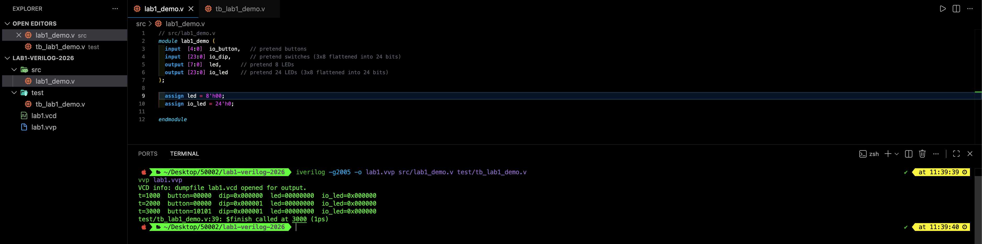
Create src/lab1_demo.v:
// src/lab1_demo.v
module lab1_demo (
  input  [4:0]  io_button,   // pretend buttons
  input  [23:0] io_dip,      // pretend switches (3x8 flattened into 24 bits)
  output [7:0]  led,      // pretend 8 LEDs
  output [23:0] io_led    // pretend 24 LEDs (3x8 flattened into 24 bits)
);

  assign led   = 8'h00;
  assign io_led = 24'h0;

endmodule
This module is not connected to real hardware. It just produces output signals that we can observe in simulation. Right now, we just assign led and io_led to a constant 0, we have yet to use the input. We will do that later, let’s simulate first.
Testbench: drive inputs and print outputs
Create test/tb_lab1_demo.v:
// test/tb_lab1_demo.v
`timescale 1ns/1ps

module tb_lab1_demo;
  reg  [4:0]  io_button;
  reg  [23:0] io_dip;
  wire [7:0]  led;
  wire [23:0] io_led;

  lab1_demo dut (
    .io_button(io_button),
    .io_dip(io_dip),
    .led(led),
    .io_led(io_led)
  );

  task show;
    begin
      $display("t=%0t  button=%b  dip=0x%h  led=%b  io_led=0x%h",
               $time, io_button, io_dip, led, io_led);
    end
  endtask

  initial begin
    // waveform dump for later (Vapor)
    $dumpfile("lab1.vcd");
    $dumpvars(0, tb_lab1_demo);

    io_button = 5'b00000;
    io_dip    = 24'h000000;
    #1; show();

    io_dip[0] = 1'b1;
    #1; show();

    io_button = 5'b10101;
    #1; show();

    $finish;
  end
endmodule
Running vvp lab1.vvp prints the signal values. It also writes lab1.vcd waveform which we will use later with Vapor.
Testbench walkthrough
This file is a testbench. It is a Verilog module written for simulation only. A testbench is not meant to be synthesized into hardware. Its job is to:
- Provide input values to the design-under-test (DUT)
- Observe the DUT outputs
- Print or record those outputs so you can verify behavior
timescale
At the top, we can always define the timescale of our simulation. It is common to write:
`timescale 1ns/1ps
This sets the simulation time unit and precision:
1nsmeans#1is 1 nanosecond1psmeans the simulator can represent time down to 1 picosecond resolution
The testbench module has no ports
module tb_lab1_demo;
A testbench typically has no input/output ports because nothing outside “connects” to it: no switches, no LEDs, no 7 Segments. It is the top-level for the simulator.
Internal wiring
We usereg for inputs we drive, wire for outputs we observe
reg  [4:0]  io_button;
reg  [23:0] io_dip;
wire [7:0]  led;
wire [23:0] io_led;
io_buttonandio_dipare declared asregbecause the testbench assigns them in procedural code (initialblock).ledandio_ledarewirebecause they are driven by the DUT’s outputs.
Recap
Procedural assignment requires a variable type (
reg), while module outputs are nets (wire) from the testbench point of view.
Instantiation: creating the DUT and connecting ports
lab1_demo dut (
  .io_button(io_button),
  .io_dip(io_dip),
  .led(led),
  .io_led(io_led)
);
This instantiates the module lab1_demo (defined in ../src/lab1_demo.v) and names this instance dut.
The .(port)(signal) syntax is named port connection:
.io_button(io_button)means: connect the DUT portio_buttonto the testbench signalio_button- and so on for the other ports
Recap
Named port connections are the safer style because the wiring does not depend on port order.
A small helper function: task show
  task show;
    begin
      $display("t=%0t  button=%b  dip=0x%h  led=%b  io_led=0x%h",
               $time, io_button, io_dip, led, io_led);
    end
  endtask
A task is like a small reusable procedure in Verilog, kinda like a function. It is just a way to avoid repeating the same $display line many times.
$displayprints one line to the console%0tprints simulation time ($time)%bprints in binary%hprints in hex
Printing in Simulation
This is how we “observe LEDs” in simulation: we print the output bit patterns.
The stimulus: initial begin ... end
In a testbench, initial is where you write your stimulus sequence. This is the sequential code that “runs” the simulation.
  initial begin
    // waveform dump for later (Vapor)
    $dumpfile("lab1.vcd");
    $dumpvars(0, tb_lab1_demo);

    io_button = 5'b00000;
    io_dip    = 24'h000000;
    #1; show();

    io_dip[0] = 1'b1;
    #1; show();

    io_button = 5'b10101;
    #1; show();

    $finish;
  end
An initial block runs once at time t=0 when the simulator starts. It works sequentially (like plain software code, not hardware code). This is what each line does:
$dumpfile("lab1.vcd")selects the waveform output file name$dumpvars(0, tb_lab1_demo)tells the simulator what signals to record into the waveform file- The assignments set the testbench inputs to known values
#1;advances simulation time by 1ns (because oftimescale)show();prints the current input/output values$finish;ends the simulation
Add a tiny delay with #1
After changing inputs to DUTs in the testbench, we should insert a tiny delay (e.g.,
#1) before checking outputs. This gives the simulator one step to re-evaluate the DUT so the outputs have “settled”. Use#1for a simple real-time wait (1 ns here).When testing sequential logic in the later weeks, there’s some subtle tweaks. We will explain to you later on.
Refer to the appendix section if you’d like to know more about how to write a testbench. We will also cover this in the next lab.
Simulation Duration
In Icarus, the simulation runs until something ends it, typically:
- the first
$finish;, or - there are no more scheduled events left to process
If you have the following testbench:
io_button = 5'b00000;
io_dip    = 24'h000000;
#1; show();

$finish;
- The
initialblock starts at t = 0 #1advances time by 1 ns (because of`timescale 1ns/1ps)- Then it calls
show()at t = 1 ns - Then
$finishends the simulation
So it simulates up to t = 1 ns (plus some zero-time “delta cycles” the simulator uses internally, but wall-clock simulation time is 1 ns).
If you later add a loop like:
for (i = 0; i < 16; i = i + 1) begin
  io_dip = i;
  #1;
end
$finish;
Then it ends at t = 16 ns.
Total simulated time is the sum of all #<delay> steps that occur before $finish.
Therefore in our testbench above tb_lab1_demo.v, we simulate at least 3000ps (3ns).
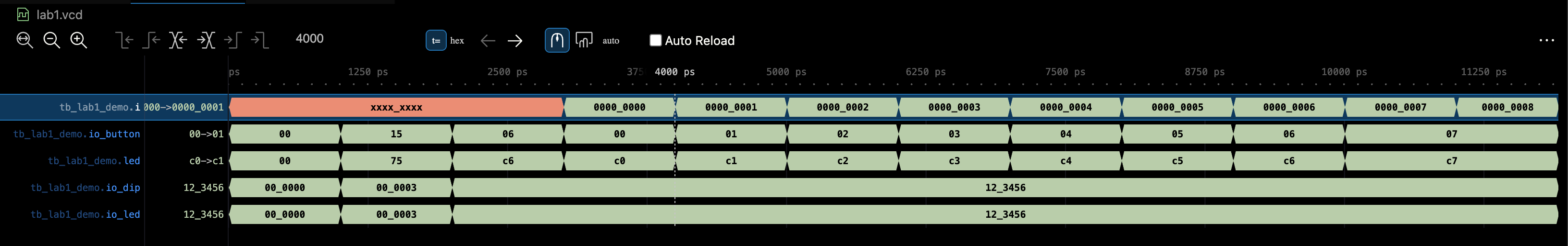
Viewing the .vcd file
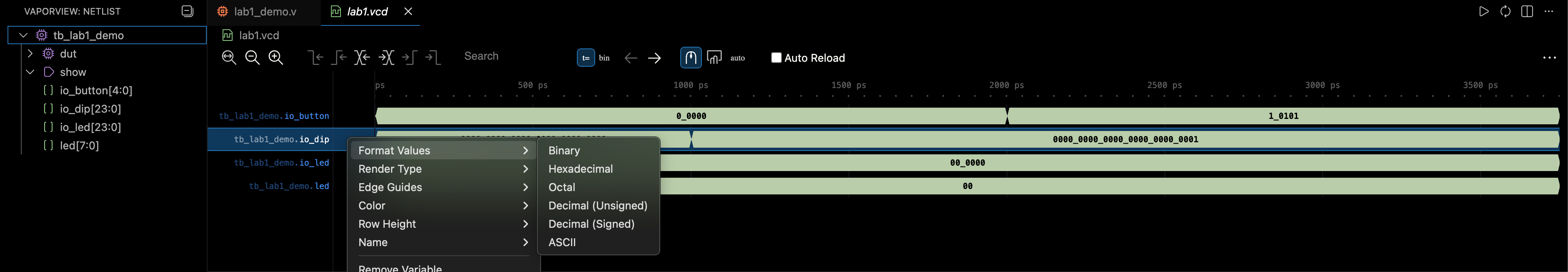
You can open the vcd file to view the waveform with extensions like VaporView.
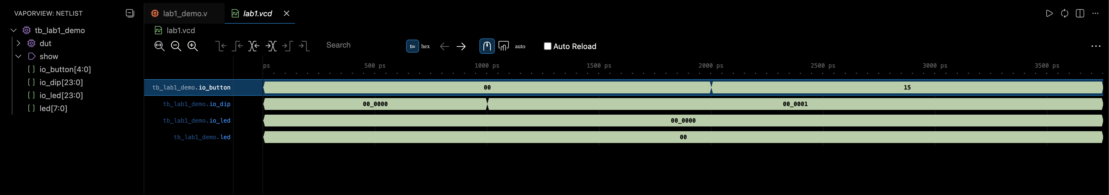
- We can add variables to the plot to inspect as we wish. Here we add all 4 from the testbench file
- The values are set to be displayed in hex (you can right click on the graph and change the viewing mode to decimal, binary, etc)
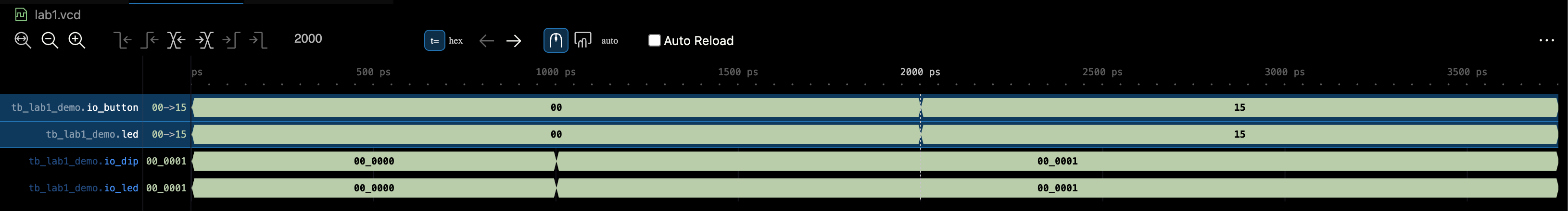
- At 2ns above,
io_buttonis set to0x15(5’b10101`), which match what we set in the testbench io_ledandledvalues are undetermined (red bars) because we didn’t set it in the testbench
About parameters (not used yet)
This testbench does not use parameters, but you will see something like this later:
some_module #(.WIDTH(8)) inst_name ( ... );
That means: instantiate some_module with a parameter override. We will use that in the next lab when we start building reusable multi-bit modules.
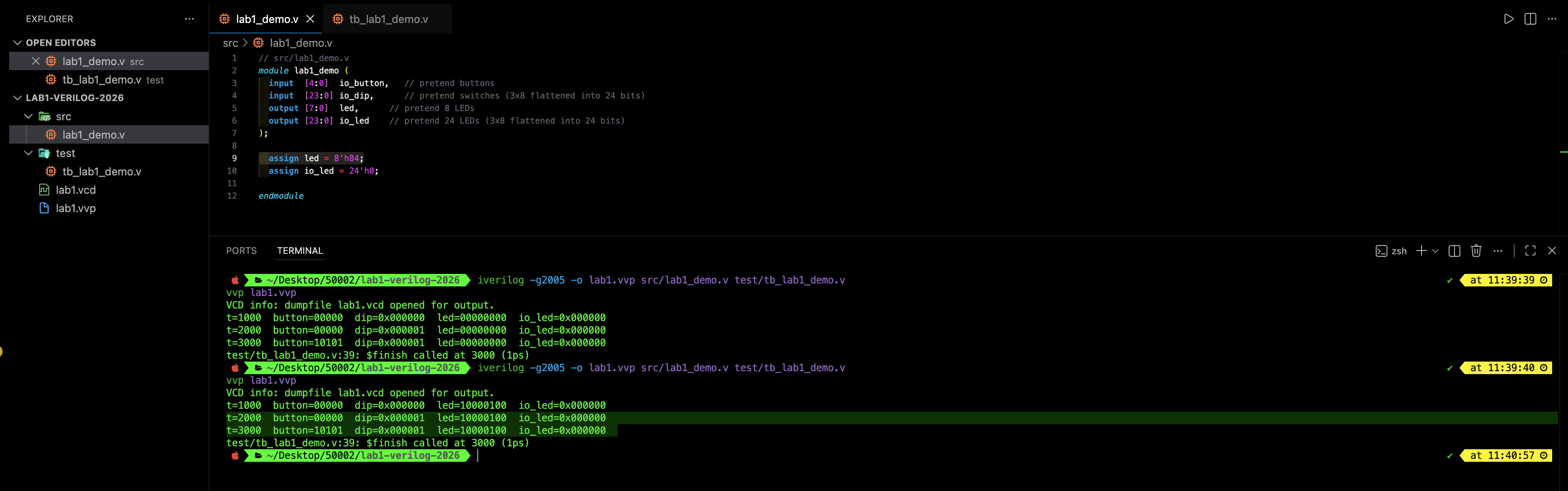
Change LED value
Right now, led = 8'h00, so all 8 bits are 0.
To turn on the rightmost LED bit, change the assignment in lab1_demo.v:
led = 8'b00000001;
Try other patterns (choose one):
led = 8'b10000000;
led = 8'h80;
led = 8'd10;
led = 8'h84;
Value assignment
In Verilog, constants usually follow this format:
<width>'<base><value>
Examples:
8'b00000001   // 8 bits, binary
8'h84         // 8 bits, hexadecimal
8'd10         // 8 bits, decimal
Understanding the bases
These represent the same 8-bit pattern:
| Syntax | Meaning | Binary form |
|---|---|---|
8'b00001010 |
8-bit binary | 00001010 |
8'h0A |
8-bit hexadecimal | 00001010 |
8'd10 |
8-bit decimal | 00001010 |
Width Matters
Verilog allows unsized numbers like:
led = 12;
In Verilog, an unsized decimal like 12 is treated as a 32-bit constant, then assigned into led[7:0] using truncation rules (see below).
For small values, this often appears to “work”, but it can hide cases where bits are silently discarded. Good practice is to always write widths when driving hardware-sized signals:
led = 8'd12;
Unsized numbers can trigger silent resizing (see section below on truncation) and sign-extension rules. For this course, always write widths when driving buses. For predictable hardware, prefer sized constants.
Named Constants
If you want to name constants, use localparam:
localparam [7:0]  LED_OFF   = 8'h00;
localparam [7:0]  LED_DEMO  = 8'h84;
localparam [23:0] IOLED_OFF = 24'h0;
You can use localparam anywhere you would normally write a literal.
module lab1_demo (
  input  [4:0]  io_button,
  input  [23:0] io_dip,
  output [7:0]  led,
  output [23:0] io_led
);
  localparam [7:0]  LED_PREFIX = 8'b0000_0000;
  localparam [23:0] IOLED_OFF  = 24'h0;

  assign led    = LED_PREFIX;
  assign io_led = IOLED_OFF;
endmodule
Multiple value settings in an always @* block
Similarly, assign an always @* begin ... end, later assignments override earlier ones when they target the same bits.
Example:
always @* begin
  led = 8'b00000000;
  led[0] = 1'b1;
end
Final value of led (8 bits) is set to be 00000001. Assignments in always block in HDL is NOT about time passing. It is how priority is expressed when multiple statements drive the same signal in the same combinational block.
Inputs, interactivity, and bit-flow in Simulation
Since we are not using the Alchitry IO panel here, “buttons” and “switches” are just input signals that the testbench drives.
Update lab1_demo.v to connect inputs to outputs.
// src/lab1_demo.v
module lab1_demo (
  input  [4:0]  io_button,   // pretend buttons
  input  [23:0] io_dip,      // pretend switches (3x8 flattened into 24 bits)
  output [7:0]  led,      // pretend 8 LEDs
  output [23:0] io_led    // pretend 24 LEDs (3x8 flattened into 24 bits)
);


  assign led = {3'b000, io_button};      // led[7:5]=000, led[4:0]=io_button
  assign io_led = io_dip ;

endmodule
Now, changing io_button and io_dip inside the testbench will immediately change led and io_led. In this screenshot below, we see how the led values follow io_button fed by the testbench, and how io_led values follow the io_dip values accordingly.
Illegal multiple assign
Do NOT have multiple assign statements driving the same net. It’s not going to take precedence with the last one like in always block. Read more about this in the appendix.
This is what happens if we have multiple assign, you have x (undetermined) values at the led and io_led because the drivers have conflicting values.
Every output must be driven
In simulation, if an output is never assigned, it will show up as x (unknown). That is the simulator telling you the signal has no defined driver. In real hardware, an undriven output is not meaningful either. You cannot “leave a pin floating” and expect deterministic behavior.
This most commonly happens when:
- you declare many output ports but forget to drive some of them,
- you use an
always @*block but only assign outputs in some branches (ifwithoutelse, incompletecase, etc.)
// src/lab1_demo.v  (BAD)
module lab1_demo (
  input  [4:0]  io_button,
  input  [23:0] io_dip,
  output [7:0]  led,
  output [23:0] io_led
);

  // led is driven
  assign led = {3'b000, io_button};

  // io_led is NOT driven at all
  // assign io_led = ...;   // forgot

endmodule
What you will see:
ledfollowsio_buttonio_ledstays xxxxxxxxxxxxxxxxxxxxxxxx in waveform and prints
Always ensure that you have complete assignment and practice good static discipline.
always @* evaluation
In a testbench, always @* re-evaluates when something in its auto-generated sensitivity list changes. That list is built from signals that are read on the right-hand side inside the block.
If we have a block like this:
// src/lab1_demo.v
module lab1_demo (
  input  [4:0]  io_button,   // pretend buttons
  input  [23:0] io_dip,      // pretend switches (3x8 flattened into 24 bits)
  output reg [7:0]  led,      // pretend 8 LEDs
  output reg [23:0] io_led    // pretend 24 LEDs (3x8 flattened into 24 bits)
);

  always @* begin
    led = 8'h4;
    io_led = 24'h1;
  end

endmodule
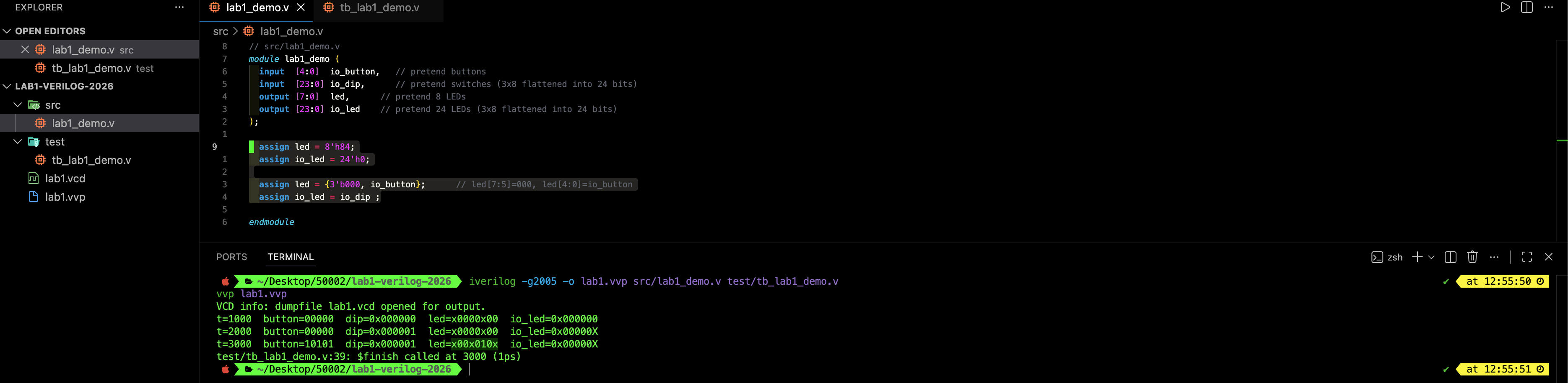
there are no reads at all in that entire always block, only constant writes. So the inferred sensitivity list is effectively empty. In Icarus, that means that always block never triggers, so led and io_led stay at their default uninitialized value, which is x.
Therefore if the output ALWAYS constant for the entire block, the clean way is to use continuous assignments (assign) and keep the outputs as plain wire-style outputs. This is what we did before.
// src/lab1_demo.v  (CONSTANT OUTPUTS)
module lab1_demo (
  input  [4:0]  io_button,   // unused for now
  input  [23:0] io_dip,      // unused for now
  output [7:0]  led,
  output [23:0] io_led
);

  assign led    = 8'h04;
  assign io_led = 24'h000001;

endmodule
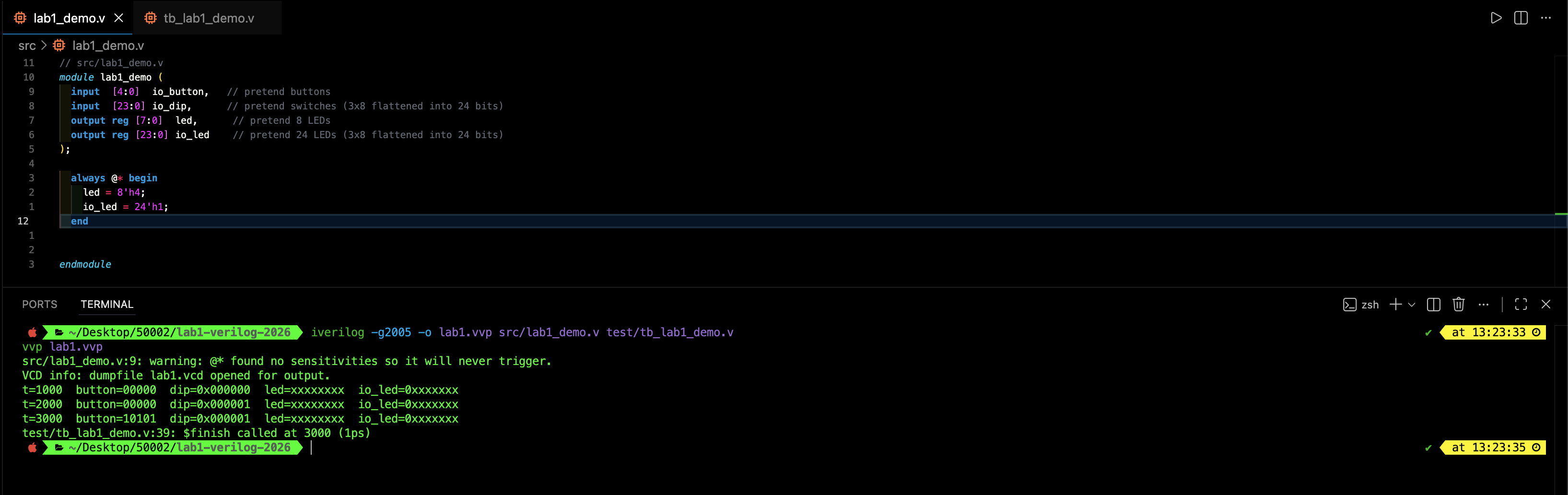
To stress the point further: this code works as expected because now the always @* block reads an input (io_dip) on the right-hand side. Recall how we need to declare reg in the output port because now we assign its value in the always block.
Recap
If a signal is assigned inside an
alwaysblock, it must be a variable type, so it needs to be declared asreg.
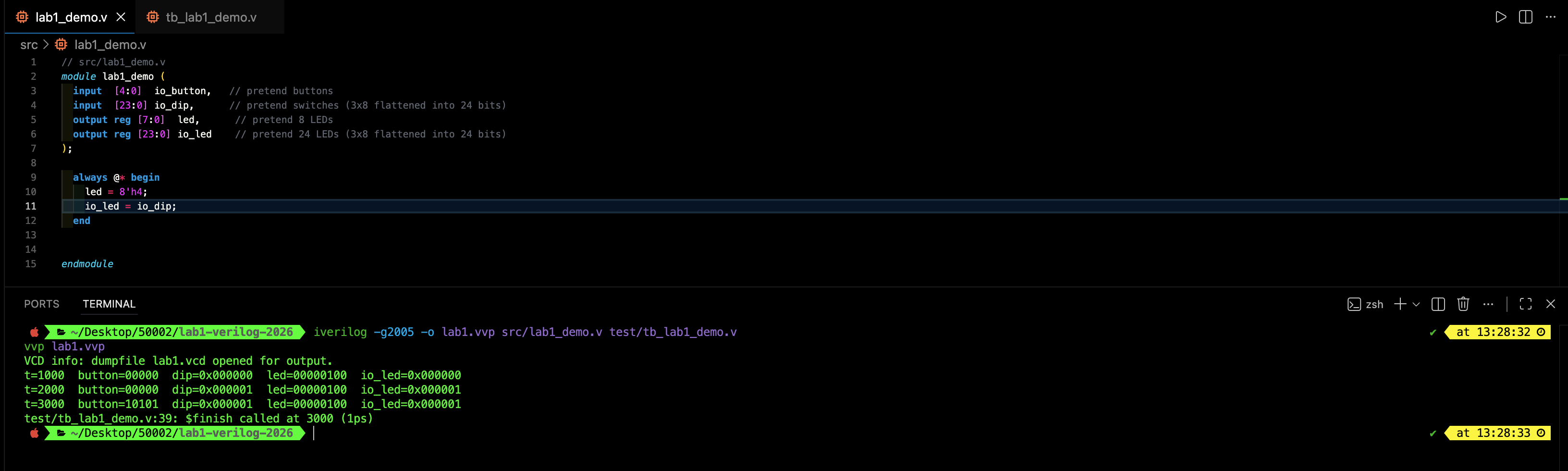
// src/lab1_demo.v
module lab1_demo (
  input  [4:0]  io_button,   // pretend buttons
  input  [23:0] io_dip,      // pretend switches (3x8 flattened into 24 bits)
  output reg [7:0]  led,      // pretend 8 LEDs
  output reg [23:0] io_led    // pretend 24 LEDs (3x8 flattened into 24 bits)
);

  always @* begin
    led = 8'h4;
    io_led = io_dip;
  end

endmodule
That single read is enough for @* to build a non-empty sensitivity list that includes io_dip. As soon as the testbench assigns io_dip (including at time 0), io_dip changes value and the block triggers, so both io_led and led get assigned.
If we had written another form always @(/* empty */), this does execute once at t = 0 and then never again. always @* explicitly replaces that pattern with automatic sensitivity, and when it infers an empty list, it truly never fires. This is how most simulators actually behave, but to be really sure you should check with the documentation.
Arrays in Verilog
In Verilog, an “array” or “bus” is not an abstract data structure. It is a fixed set of signals, like a bundle of wires.
A vector like wire [7:0] led is literally eight wires bundled together, and a “2D-style” array like reg [7:0] row [0:2] is three bundles of eight wires (24 wires total). When you concatenate or slice ({array1, array2}, [3:0], etc.), you are selecting and wiring specific bits from those bundles*.
Nothing stretches or shrinks at runtime. If widths do not match, Verilog will apply its truncation/extension rules (see below), which may compile but can silently change which wires are actually connected.
The following sections about array manipulation is actually the materials of later labs, but it is essential to introduce it now for the Verilog version since we are working with flattened arrays due to reasons listed below.
Array replication (duplication) and concatenation
Verilog uses the following syntax for:
- concatenation:
{a, b, c} - replication:
{N{a}}(note the braces around replication)
Example (24-bit “3×8 all zeros”):
io_led = {3{8'h00}}; // 8'h00 repeated 3 times
Example (only the last 8-bit group is 1):
io_led = {8'h00, 8'h00, 8'h01};
Concatenation order matters. In {led2, led1, led0}, led2 becomes the top 8 bits [23:16], led1 becomes [15:8], and led0 becomes the bottom 8 bits [7:0].
2D Arrays
Lucid supports 2D buses directly in the port list, such as io_dip[3][8]. Verilog can represent “2D-like” structures too, but the syntax and tool support are less uniform, especially for module ports.
In this lab, we did a “workaround” by flattening that into a single 24-bit bus:
- row 0:
io_dip[7:0] - row 1:
io_dip[15:8] - row 2:
io_dip[23:16]
Bit slicing (selecting sub-buses)
This is a direct part-select:
wire [7:0] row0 = io_dip[7:0];
wire [7:0] row1 = io_dip[15:8];
wire [7:0] row2 = io_dip[23:16];
And this is an indexed part-select:
wire [7:0] row0b = io_dip[0  +: 8];   // 8 bits starting at bit 0
wire [7:0] row2b = io_dip[16 +: 8];   // 8 bits starting at bit 16
base +: width means “take width bits starting from base going upward”. There is also base -: width for selecting downward.
You can also use localparams (named constants) to define bit positions when slicing:
localparam integer LED_AND = 5;
localparam integer LED_OR  = 6;
localparam integer LED_XOR = 7;

always @* begin
  led = 8'h00;
  led[LED_AND] = io_dip[0] & io_dip[1];
  led[LED_OR]  = io_dip[0] | io_dip[1];
  led[LED_XOR] = io_dip[0] ^ io_dip[1];
end
Array of vectors
In Verilog-2001, the most common way to model a 2D structure is an array of 1D vectors (often used for memories, but it also works for small row arrays). We can define such 2D internal signals:
reg  [7:0] io_dip [0:2];   // 3 rows, each row is 8 bits
wire [7:0] io_led [0:2];   // 3 rows, each row is 8 bits
This gives you exactly what you want conceptually:
io_dip[0]is an 8-bit rowio_dip[1]is an 8-bit rowio_dip[2]is an 8-bit row
Example use:
assign io_led[0] = io_dip[0]; // “row 0 LEDs show row 0 switches”
Toolchain Inconsistencies
However, these 2D arrays are awkward on module ports. Inside a module, 2D arrays are fine. The annoying issue appears when you try to place them in the port list and pass them between modules because some tools accept this style, others are picky, and it becomes harder to keep the lab setup consistent across Windows/macOS/Linux toolchains.
So while you can write code that looks like a Lucid port list, it is not the most reliable choice for a portable Verilog code.
Flatten at ports
The simplest cross-tool method is:
- Keep the port as a single flat bus (24 bits)
- Slice it into 8-bit “rows” internally
- Concatenate rows back into a flat output bus
// flat input bus
input  [23:0] io_dip;
output [23:0] io_led;

// row views (8-bit each)
wire [7:0] dip0 = io_dip[7:0];
wire [7:0] dip1 = io_dip[15:8];
wire [7:0] dip2 = io_dip[23:16];

wire [7:0] led0;
wire [7:0] led1;
wire [7:0] led2;

assign led0 = dip0;
assign led1 = 8'h00;
assign led2 = 8'h00;

// pack rows back into 24-bit output
assign io_led = {led2, led1, led0};
This preserves the “3×8 rows” idea while avoiding 2D-port tool issues.
Logic Gates (AND / OR / XOR) in Verilog
Essential Verilog Operators
This section uses a small subset of Verilog operators like boolean, bitwise, reduction, and some arithmetic. The key idea is that many operators work on 1-bit signals or on buses, and some operators produce a 1-bit true/false result. Most of them are self-explanatory, but you can view the appendix section if needed.
In lecture, logic gates are introduced using truth tables. In Verilog, we usually do not build gates explicitly. Instead, we write Boolean expressions, and the synthesis tool maps them to FPGA hardware. The logic itself is the same.
Single-bit logic gates in Verilog use bitwise operators:
| Gate | Operator | Description |
|---|---|---|
| AND | & |
Output is 1 only if both inputs are 1 |
| OR | | |
Output is 1 if either input is 1 |
| XOR | ^ |
Output is 1 if the inputs are different |
| NOT | ~ |
Bitwise invert (recommended for “gate NOT”) |
You are probably familiar with !, which is a logical NOT (it reduces to 1-bit true/false), and not bitwise. For 1-bit signals, !a and ~a often behave the same, but for “gate thinking”, use ~.
Exploring gates using DIP switches
Use two DIP switches as logic inputs, then drive three LEDs using different logic gates like so.
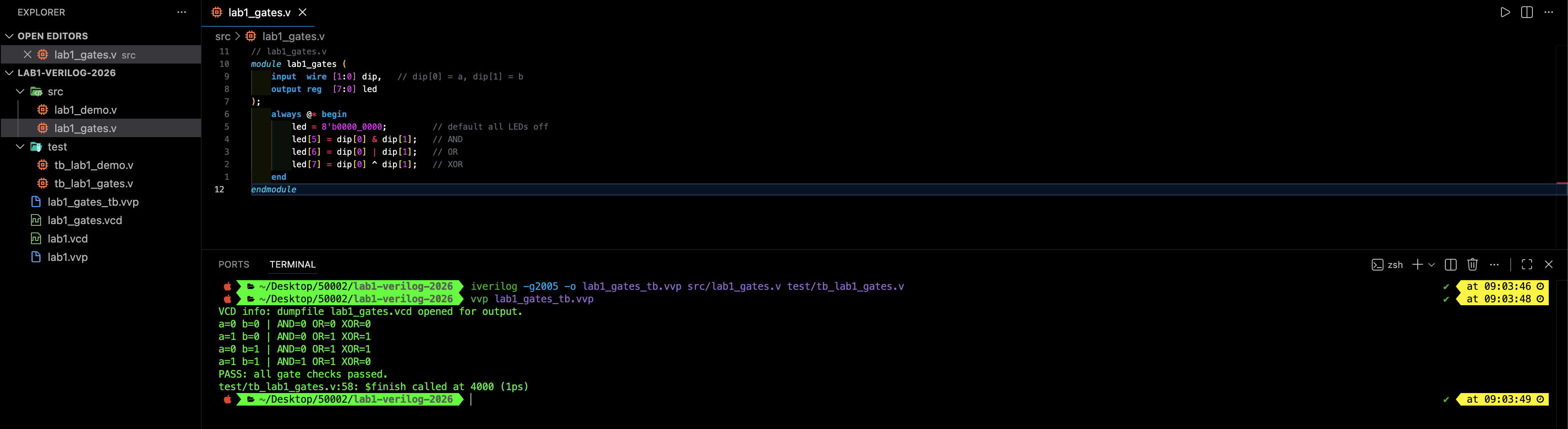
Example module (maps dip[0] and dip[1] to led[5..7]):
// src/lab1_gates.v
module lab1_gates (
    input  wire [1:0] dip,   // dip[0] = a, dip[1] = b
    output reg  [7:0] led
);
    always @* begin
        led = 8'b0000_0000;         // default all LEDs off
        led[5] = dip[0] & dip[1];   // AND
        led[6] = dip[0] | dip[1];   // OR
        led[7] = dip[0] ^ dip[1];   // XOR
    end
endmodule
We can toggle the dip values using a testbench through all four input combinations and verify the led outputs match the truth table.
| a | b | AND | OR | XOR |
|---|---|---|---|---|
| 0 | 0 | 0 | 0 | 0 |
| 0 | 1 | 0 | 1 | 1 |
| 1 | 0 | 0 | 1 | 1 |
| 1 | 1 | 1 | 1 | 0 |
This testbench runs all 4 input cases and checks led[5], led[6], led[7].
// test/tb_lab1_gates.v
`timescale 1ns/1ps

module tb_lab1_gates;
    reg  [1:0] dip;
    wire [7:0] led;

    integer i;
    integer errors;

    // Device Under Test
    lab1_gates dut (
        .dip(dip),
        .led(led)
    );

    initial begin
        errors = 0;

        // Optional waveform dump
        $dumpfile("lab1_gates.vcd");
        $dumpvars(0, tb_lab1_gates);

        // Try all 4 combinations: 00, 01, 10, 11
        for (i = 0; i < 4; i = i + 1) begin
            dip = i[1:0];
            #1; // allow combinational logic to re-evaluate (delta cycle)

            // Expected results (a = dip[0], b = dip[1])
            if (led[5] !== (dip[0] & dip[1])) begin
                $display("FAIL AND: a=%0d b=%0d led[5]=%0d expected=%0d",
                         dip[0], dip[1], led[5], (dip[0] & dip[1]));
                errors = errors + 1;
            end

            if (led[6] !== (dip[0] | dip[1])) begin
                $display("FAIL OR : a=%0d b=%0d led[6]=%0d expected=%0d",
                         dip[0], dip[1], led[6], (dip[0] | dip[1]));
                errors = errors + 1;
            end

            if (led[7] !== (dip[0] ^ dip[1])) begin
                $display("FAIL XOR: a=%0d b=%0d led[7]=%0d expected=%0d",
                         dip[0], dip[1], led[7], (dip[0] ^ dip[1]));
                errors = errors + 1;
            end

            $display("a=%0d b=%0d | AND=%0d OR=%0d XOR=%0d",
                     dip[0], dip[1], led[5], led[6], led[7]);
        end

        if (errors == 0) begin
            $display("PASS: all gate checks passed.");
        end else begin
            $display("FAIL: %0d errors.", errors);
        end

        $finish;
    end
endmodule
Run with Icarus Verilog (Verilog-2005) as usual:
iverilog -g2005 -o lab1_gates_tb.vvp src/lab1_gates.v test/tb_lab1_gates.v
vvp lab1_gates_tb.vvp

Logic gates are not written as modules
In FPGA designs, you typically do not create separate AND/OR/XOR “gate modules”. The FPGA fabric already implements logic internally, and writing Boolean expressions directly is clearer and scales better.
For example, an AND gate as a standalone module is functionally correct, but awkward:
module and2 (
    input  wire a,
    input  wire b,
    output wire y
);
    assign y = a & b;
endmodule
Using it adds noise:
wire y_and;

and2 g_and (
    .a(dip[0]),
    .b(dip[1]),
    .y(y_and)
);

// then later: led[5] = y_and (via assign/always)
Instead, write the logic directly where you need it:
// direct expression (recommended)
led[5] = dip[0] & dip[1];
In later labs, you will build larger modules such as adders, multiplexers, and state machines, not individual logic gates.
Putting it all together
Now is the time to do the following to practice what we learned above:
- uses a flattened 24-bit bus to represent a 3×8 “2D-style” signal
- slices it into 8-bit rows internally
- concatenates rows back to a 24-bit output
- uses concatenation to pack io_button into the lower 5 bits of led
- generates a VCD waveform you can inspect later
Study the following demo code:
// src/lab1_demo.v
module lab1_demo (
  input  [4:0]  io_button,  // pretend buttons
  input  [23:0] io_dip,     // pretend switches (3x8 flattened into 24 bits)
  output reg [7:0]  led,    // pretend 8 LEDs
  output reg [23:0] io_led  // pretend 24 LEDs (3x8 flattened into 24 bits)
);

  // Named constants (localparams) are the usual way to define widths and indices.
  localparam integer ROW_W   = 8;
  localparam integer LED_AND = 5;
  localparam integer LED_OR  = 6;
  localparam integer LED_XOR = 7;

  // Slice the 24-bit input into three 8-bit "rows".
  // Indexed part-select: base +: width
  wire [ROW_W-1:0] dip0 = io_dip[0*ROW_W +: ROW_W];  // bits [7:0]
  wire [ROW_W-1:0] dip1 = io_dip[1*ROW_W +: ROW_W];  // bits [15:8]
  wire [ROW_W-1:0] dip2 = io_dip[2*ROW_W +: ROW_W];  // bits [23:16]

  // Combinational gates from two switch bits (row 0, bits 0 and 1)
  wire gate_and = dip0[0] & dip0[1];
  wire gate_or  = dip0[0] | dip0[1];
  wire gate_xor = dip0[0] ^ dip0[1];

  always @* begin
    // Defaults: every output gets a value
    led   = 8'h00;
    io_led = 24'h0;

    // “Inputs drive outputs” mapping
    led[4:0] = io_button;       // upper 3 bits remain 0 unless overridden below
    io_led   = io_dip;          // flat copy (same as {dip2, dip1, dip0})

    // Override specific LED bits with gate outputs
    led[LED_AND] = gate_and;
    led[LED_OR]  = gate_or;
    led[LED_XOR] = gate_xor;
  end

endmodule
Then let’s have a more comprehensive test bench:
// test/tb_lab1_demo.v
`timescale 1ns/1ps

module tb_lab1_demo;
  reg  [4:0]  io_button;
  reg  [23:0] io_dip;
  wire [7:0]  led;
  wire [23:0] io_led;

  lab1_demo dut (
    .io_button(io_button),
    .io_dip(io_dip),
    .led(led),
    .io_led(io_led)
  );

  task show;
    begin
      $display("t=%0t  button=%b  dip=0x%h  led=%b  io_led=0x%h",
               $time, io_button, io_dip, led, io_led);
    end
  endtask

  integer i;

  initial begin
    $dumpfile("lab1.vcd");
    $dumpvars(0, tb_lab1_demo);

    // Start with known inputs
    io_button = 5'b00000;
    io_dip    = 24'h000000;
    #1; show();

    // Set dip row 0 bits [1:0] = 2'b11 so AND/OR/XOR become 1/1/0
    // Format is {row2, row1, row0}
    io_button = 5'b10101;
    io_dip    = {8'h00, 8'h00, 8'h03};
    #1; show();

    // A more "random-looking" pattern
    io_button = 5'b00110;
    io_dip    = {8'h12, 8'h34, 8'h56};
    #1; show();

    // Small sweep of button patterns (purely to generate more waveform transitions)
    for (i = 0; i < 8; i = i + 1) begin
      io_button = i[4:0];
      #1; show();
    end

    $finish;
  end
endmodule
Compiling and running the code above should give you:
Open lab1.vcd in your waveform viewer later and inspect:
io_buttonchanging over timeled[4:0]matchingio_buttonled[7:5]changing based onio_diprow0bits[1:0]io_ledmatchingio_dip(same bits, just repacked through slices and concatenation)
How long does this simulation run for?
This testbench advances time using #1 delays and ends at $finish. In the code above:
- 3 explicit #1 steps
- 8 loop iterations, each has
#1Total simulated time is about 11 ns, and it ends exactly when$finishexecutes.
Auto truncation, auto extension, and width mismatches
Verilog will silently resize values to make an assignment fit. This is convenient, but it also means you can wire the wrong bits without getting an error.
Truncation (wide RHS to narrow LHS)
If the RHS has more bits than the LHS, Verilog keeps the least-significant bits and discards the extra most-significant bits.
wire [7:0] a;
assign a = 16'h12AB;   // RHS is 16 bits, LHS is 8 bits

// a becomes 8'hAB   (the top 8 bits 16'h12 are discarded)
Another common accidental case is assigning an 8-bit bus into a 5-bit field:
wire [4:0] b;
assign b = 8'b1010_1100;   // b becomes 5'b0_1100 (LSBs kept)
Extension (narrow RHS to wide LHS)
If the RHS has fewer bits than the LHS, Verilog extends it to match the LHS width.
wire [7:0] c;
assign c = 4'hF;        // RHS is 4 bits: 1111

// c becomes 8'h0F  (upper bits filled with 0)
This often happens when you forget to write a width:
wire [7:0] d;
assign d = 12;          // unsized decimal literal (special case)
Unsized number literals in Verilog have rules that surprise beginners. In practice, do not rely on implicit sizing. Prefer:
assign d = 8'd12;
Danger to beginners
A width mismatch still produces SOME wiring, so simulation “works”, but it may not be the wiring you intended.
Example: You meant to light LED bit 7 only, but accidentally wrote a 9-bit value:
wire [7:0] led;
assign led = 9'b1_0000_0000;   // 9 bits, LHS is 8 bits

// truncation keeps the lower 8 bits -> led becomes 8'b0000_0000 (all off)
Example: You meant an 8-bit hex constant but forgot the width:
wire [7:0] led;
assign led = 'h80;   // In plain Verilog, this is not a safe habit.
You should use explicit widths as stated above.
assign led = 8'h80;
Good value assignment habits
- Always write widths on constants that drive buses:
8'h84,24'h0,5'b10101.- When combining signals, make the width obvious with concatenation:
assign led = {3'b000, io_button}- When selecting bits from a wider bus, slice explicitly:
assign io_led[7:0] = io_dip[7:0]
If you cannot clearly state which bits on the RHS end up on which wires on the LHS, treat the assignment as suspect even if it compiles.
A Very Dangerous Bug
This happens when there’s a module input width. Suppose a submodule expects an 8-bit input:
module child (
  input  [7:0] in,
  output       y
);
  assign y = ∈   // y=1 only if all 8 bits are 1
endmodule
Now in the parent, you intended to feed the SAME 1-bit signal into all 8 bits.
A correct way to do this is to replicate 1 bit into 8 bits:
wire SIGNAL;          // 1 bit
wire y;

child u0 (
  .in({8{SIGNAL}}),   // 8 copies of SIGNAL
  .y(y)
);
If SIGNAL=1, then in=8'b11111111 and y=1.
If SIGNAL=0, then in=8'b00000000 and y=0.
However it is common to make this mistake. The code will succesfully compile due to auto-extension:
child u0 (
  .in(SIGNAL),   // SIGNAL is 1 bit, but in is 8 bits
  .y(y)
);
Verilog will extend the 1-bit RHS to 8 bits. In most contexts, it becomes:
SIGNAL=1:in = 8'b00000001SIGNAL=0:in = 8'b00000000
So y becomes 0 even when SIGNAL=1, because &in is only 1 when all bits are 1. You accidentally wired only the LSB to your signal, and the other 7 bits got filled with zeros.
This is a classic HDL bug as the code compiles, but the hardware does not behave the way you wanted it to. If you mean “copy this bit into a whole bus”, you must write replication explicitly: {N{bit}}.
Other always forms (preview)
always @* is not the only pattern of the always block. In Verilog there are many different types. Here are some for your knowledge.
Old-style combinational sensitivity list (manual)
Example
// Combinational (manual list): re-evaluates when any listed signal changes
always @(a or b or sel) begin
  if (sel) y = a;
  else     y = b;
end
Explanation
This is the older style of writing combinational logic: you must manually list every signal that affects the result. If you forget one, simulation can miss updates. That is why modern code uses always @* instead.
Clocked sequential logic (a register)
Example
// Sequential: updates only on rising clock edges
always @(posedge clk) begin
  q <= d;
end
Explanation
This models a flip-flop. The block runs only on posedge clk. Use <= (nonblocking) for registers so multiple registers update together at the clock edge.
Clocked logic with asynchronous reset
Example
// Async reset: reset can take effect immediately, not waiting for the clock
always @(posedge clk or posedge rst) begin
  if (rst) q <= 1'b0;
  else     q <= d;
end
Explanation
The event control says: run the block on either a clock edge or a reset edge. This is a standard pattern you will see later when we add reset behavior.
Testbench-only periodic always (clock generator)
Example
// Testbench clock generator (not meant for synthesis)
always #5 clk = ~clk;   // toggles every 5 time units
Explanation
This is procedural simulation stimulus. It schedules events with delays (#5). It is great for testbenches, but it is not describing combinational logic or “real hardware wiring” the way assign or always @* does.
Plain always begin ... end (avoid in this course)
Example
// Usually a bad idea unless you REALLY know what you are doing
always begin
  // no event control or delay -> infinite zero-time loop
end
Explanation
Without an event control (@(...), @*) or a delay (#...), this can become an infinite zero-time loop and effectively hang the simulator. In our course style, you should always see always @* for combinational or always @(posedge clk ...) for sequential.
Note: SystemVerilog variants (FYI)
Example
// SystemVerilog (not Verilog-2005):
// always_comb, always_ff, always_latch
Explanation
If you later move to SystemVerilog, these forms add extra safety checks. For this lab we stick to Verilog-2005 (iverilog -g2005), so we use always @* and always @(posedge clk ...).
A Caveat: Evaluation Order
Combinational always is parallel hardware, but blocking (=) assignments are resolved in order.
In Verilog, the hardware you build is still just wires and gates operating in parallel. There is no “line 1 runs, then line 2 runs” at runtime. However, inside a combinational always @* block, blocking assignments (=) are evaluated in order.
That ordering affects what value is used when you read a signal in the middle of the block, even though the final result is still a purely combinational circuit.
Consider this tricky example:
module foo (
    input  wire a,
    output reg  out,
    output reg  cval
);

    wire c_value;
    counter c (.clk(1'b0), .rst(1'b0), .value(c_value));

    reg x;

    always @* begin
        x    = a;
        out  = x;

        x    = c_value;
        cval = c_value;
    end
endmodule
Even though out is assigned from x, it does not “follow” the later change to x the way pointer does in software. When the simulator and synthesis tool EVALUATE out = x;, the current value of x is the one from x = a;, so out becomes a function of a.
The later line x = c_value; overwrites x, but it does not retroactively change what out was computed from earlier in the same block.
After synthesis, the circuit is effectively equivalent to:
assign out  = a;
assign x    = c_value;
assign cval = c_value;
This is why the common best practice is “defaults first, overrides later.” If you want out to depend on c_value, you must assign x = c_value before out = x, or drive out directly from c_value.
Summary
This Verilog-track Lab 1 mirrors the Lucid version but runs in simulation only using Icarus Verilog (iverilog + vvp) plus a testbench (prints via $display and waveforms via .vcd).
It introduces Verilog modules (ports, instances, basic parameters), the wire vs reg split (nets driven by assign or module outputs, variables assigned in always/initial), and the core combinational style always @* with the static discipline (every output assigned on all paths, “default then override” to avoid latches).
It also covers practical bus handling (constants with explicit widths, concatenation/replication, flattening 3×8 into 24 bits, slicing with [15:8] and base +: width), plus common pitfalls like multiple drivers on a net (multiple assign), undriven outputs showing x, always @* depending on what signals are read, and silent truncation/extension bugs from width mismatches.
Here’s what we have covered so far:
- Tooling: write DUT + testbench, compile with
iverilog -g2005, run withvvp, inspect.vcd. - Core HDL concepts: modules, named port connections,
wirevsreg,assignvsalways @*, blocking=for combinational. - Correctness rules: one driver per signal, drive every output, complete assignments to avoid latches.
- Buses: sized literals, concatenation
{}, replication{N{}}, flatten/slice/pack 24-bit “3×8”. - Pitfalls: multiple
assignconflicts, missing drivers ->x, width mismatch truncation/extension, forgetting replication for 1-bit to N-bit.
Epilogue: How are Modules Realised?
A Verilog module is not “run” like a program. It is a circuit blueprint. When you instantiate a module, the tool creates the corresponding hardware structure inside the FPGA fabric.
- More instances usually means more LUTs / flip-flops.
- Wider buses usually means more wiring and more logic.
For this lab, you do not need to optimize any of this. The goal is to write correct combinational mappings and understand how signals are driven in simulation.
From Simulation to Real Hardware
Right now, we are simulating a standalone module using Icarus Verilog. Your “inputs” come from the testbench, and your “outputs” are observed in the waveform or printed with $display.
To connect the same logic to the FPGA board, you still need the same high-level structure you saw in the Lucid track:
- A top module that represents “the whole design on the FPGA” and exposes the external ports (clock, reset, LEDs, buttons, IO shield signals, etc.).
- Your design module (the one you are building in this Verilog track) gets instantiated inside the top module.
- The top module wires your module’s ports to the board-level ports.
- A constraint file maps those top-level ports to the actual FPGA pins that physically connect to LEDs, switches, buttons, and the IO shield.
So the difference is only where the “stimulus” comes from:
- In simulation: the testbench drives
io_button/io_dip. - On hardware: the FPGA pins (via the top module + constraints) drive
io_button/io_dip.
Alchitry Labs can still be used as the project container and build pipeline. It just will not show the Lucid-style IO simulator panel for Verilog modules. The wiring step still happens, but you validate behavior either through waveforms (simulation) or by observing real LEDs/buttons after you build and load onto the board.
Appendix
Iverilog Installation
macOS (Homebrew)
- Install Homebrew if you do not already have it.
- Install Icarus Verilog:
brew install icarus-verilog
Verify:
iverilog -V
vvp -V
Windows
Recommended: use WSL (Windows Subsystem for Linux) so your workflow matches Linux.
- Install WSL (Ubuntu).
- In the WSL terminal:
sudo apt update
sudo apt install iverilog
Verify:
iverilog -V
vvp -V
Alternative (native Windows): if you already have a working Icarus Verilog install on Windows and can run iverilog and vvp from PowerShell, that is acceptable. WSL is still recommended for consistency.
Linux (Ubuntu/Debian)
sudo apt update
sudo apt install iverilog
Verify:
iverilog -V
vvp -V
Linux (Fedora)
sudo dnf install iverilog
Verify:
iverilog -V
vvp -V
Writing Stimulus
Inside a testbench, initial is procedural code that executes in a defined order, so using a procedural like a for loop is normal and useful, and it works like a regular loop, not parallel connection as in HDL (e.g: repeat in Lucid)
It is imperative to remember that initial (testbench stimulus) is sequential simulation control. It schedules input changes over time using delays like #1.
Also, always @* (combinational logic in the DUT) describes continuous combinational logic. There is no “step-by-step” notion INSIDE the hardware it represents.
You can add a loop later to sweep many input patterns. There are two common patterns as follows.
Sweep a bus through many values
integer i;

initial begin
  $dumpfile("lab1.vcd");
  $dumpvars(0, tb_lab1_demo);

  io_button = 5'b00000;

  for (i = 0; i < 16; i = i + 1) begin
    io_dip = i;     // low bits change, rest stay 0
    #1; show();
  end

  $finish;
end
Randomized stimulus
integer k;

initial begin
  $dumpfile("lab1.vcd");
  $dumpvars(0, tb_lab1_demo);

  for (k = 0; k < 20; k = k + 1) begin
    io_button = $random;
    io_dip    = $random;
    #1; show();
  end

  $finish;
end
The DUT’s always @* will “react immediately” (in simulation terms, in the same time step) whenever the testbench assigns a new input value. The #1 delay is there so each stimulus step occurs at a different simulation time, making waveforms and printouts readable.
Multiple assign
In Verilog, we generally must not have multiple assign statements driving the same net. It is not “last one take precedence”.
If you write:
wire [7:0] led;

assign led = 8'h00;
assign led = 8'h84;
both are continuous drivers on the same wire. Verilog treats led like a net with multiple sources.
Net
In Verilog, a net is a signal type that represents a physical connection (a wire) that can be driven by one or more sources.
The result is not priority-based. It is resolved by net resolution rules, and you will often get:
- compile-time errors (common with stricter tool settings), or
xin simulation when drivers disagree, because the net is being driven to conflicting values
The correct Verilog pattern
If you want “default then override”, do it in a single driver. We have a few options.
One assign with an expression
Inline expressions are allowed:
assign led = io_button[0] ? 8'h84 : 8'h00;
Use an always @* block (procedural priority)
reg [7:0] led;

always @* begin
  led = 8'h00;        // default
  if (io_button[0])
    led = 8'h84;      // override if condition true
end
Here, “last assignment wins” is true within the same procedural block because it is procedural code assigning a single reg.
When multiple drivers are allowed
Multiple drivers make sense only when you intentionally model something like:
- tri-state buses (
assign bus = enable ? value : 1'bz;) - wired-OR / wired-AND nets (rare in modern FPGA-style coding)
For this course, we should exactly follow these rules:
- One signal should have exactly one driver.
- Use one
assignor onealways @*to drive an output.
Blocking vs nonblocking assignments
In Verilog, there are two assignment operators you will see inside procedural blocks:
=is blocking<=is nonblocking
They do not mean “fast vs slow”, and they do not change the fact that hardware is parallel. They are simulation and modeling semantics that help you describe two different kinds of hardware behavior correctly.
The key idea to keep straight is as follows:
- Hardware is parallel overall.
- But inside an
alwaysblock, Verilog is a procedural description used to define that hardware. - So, within a single
alwaysblock, the simulator executes statements in order to determine what values the block drives.
That is where “blocking” vs “nonblocking” matters.
What “blocking” means (=)
Blocking assignment (=) updates the left-hand side immediately within the procedural flow of that block. That means the next line in the same block will see the updated value.
This does not mean hardware is “running sequentially”. It means: “when the simulator evaluates this block, treat later statements as using the latest values computed earlier in the same block.”
Example: blocking in combinational logic (step-by-step calculation)
always @* begin
  y = a;        // y becomes a immediately (within this block evaluation)
  y = y & b;    // uses the updated y, so final y becomes (a & b)
end
Explanation
- This is a valid way to describe combinational logic, especially when you want to compute intermediate results.
- The final hardware is still just gates. The “step-by-step” is only a convenient way to write the logic.
Equivalent one-liner
always @* begin
  y = a & b;
end
Both have the same hardware meaning. The first version is sometimes easier to read when the expression is long.
What “nonblocking” means (<=)
Nonblocking assignment (<=) does NOT update the left-hand side immediately. Instead, it schedules the update to happen after the block finishes evaluating (conceptually, “at the end of the current time step” or “at the clock edge update”).
Within the same always block, later statements still see the old value (the value from before this block triggered), not the newly scheduled one.
This matches how real registers (dff) behave: multiple registers sample inputs at the clock edge and then update “together”.
Example: nonblocking in sequential logic (a register)
always @(posedge clk) begin
  q <= d;
end
Explanation
- This models a flip-flop: at each rising edge,
qtakes the value ofd. - If you update multiple registers in the same block,
<=ensures they behave like real hardware registers: all sample, then all update.
You might need to read the sequential logic lecture ahead to understand this.
Why always @* is still “hardware”, not “a program”
An always @* block is intended to model combinational logic: outputs are a function of current inputs.
Even though the block is written procedurally, you are still describing a circuit.
- The
always @*block is a RECIPE for how to compute the outputs from the inputs. - The simulator runs that recipe whenever an input changes.
- The resulting hardware is still parallel gates, but you wrote it as a recipe.
Because it is a recipe, it is normal (and expected) that ordering within the recipe matters for intermediate computations. That is why blocking = is the default for combinational code.
Rule of thumb (for this course)
These two rules alone prevent accidental bugs for most beginners.
Combinational block: use blocking =
always @* begin
  // use =
end
Example: “default then override” (the safest Lab 1 pattern)
always @* begin
  led = 8'h00;          // default: all off
  if (io_button[0])
    led = 8'h84;        // override whole bus
end
Explanation
- This is not “time passing”.
- This is one combinational driver that always produces a defined
led. - When
io_button[0]=0,ledstays at the default. - When
io_button[0]=1,ledbecomes8'h84.
This avoids incomplete assignments, so it avoids accidental latches.
Example: override only some bits
always @* begin
  led = 8'h00;          // default all bits
  led[4:0] = io_button; // override lower 5 bits only
end
Explanation
- You are describing wiring that ties
led[4:0]toio_button. - The remaining bits stay at the default value.
This is a clean way to make it obvious that led is always driven.
Clocked block: use nonblocking <=
always @(posedge clk) begin
  // use <=
end
You are not doing this in Lab 1, but you will see it soon. The reason it exists is to model “registers update together”.
Example: two registers updated on the same clock
always @(posedge clk) begin
  r1 <= in1;
  r2 <= in2;
end
Explanation
r1andr2both update on the same clock edge.- There is no “r1 updates first, then r2” in hardware.
<=matches that behavior.
Why using = in a clocked block is risky
The easiest way to feel the difference is: does the second line accidentally see the updated first line?
Example: broken swap with blocking =
always @(posedge clk) begin
  a = b;
  b = a;
end
Explanation
- Line 1 immediately changes
atob. - Line 2 then assigns
bfrom the newa(which is alreadyb). - Result: both end up equal, swap fails.
Example: correct swap with nonblocking <=
always @(posedge clk) begin
  a <= b;
  b <= a;
end
Explanation
- Both updates are scheduled based on old values.
- After the edge, they “commit together”.
- Result: swap works as intended.
Another common example: shift register
This example requires prior knowledge on how shift registers work. Please do your own study if you do not know what a shift register does.
The following perform a correct shift with nonblocking <=
always @(posedge clk) begin
  q0 <= in;
  q1 <= q0;
  q2 <= q1;
end
Explanation
q1gets the oldq0q2gets the oldq1- This matches a real shift register.
This example results in a wrong shift:
always @(posedge clk) begin
  q0 = in;
  q1 = q0;
  q2 = q1;
end
Explanation
q0becomesinimmediatelyq1becomes that newq0(so it becomesin)q2becomes that newq1(so it becomesin)- You lose the “shifted history”.
Operators quick reference
Bitwise and logical operators
Example: bitwise operators on 1-bit signals
// Bitwise ops on single bits behave like gate truth tables
assign y_and = a & b;
assign y_or  = a | b;
assign y_xor = a ^ b;
assign y_not = ~a;
Explanation
& | ^ ~ are bitwise operators. On 1-bit signals, they match the usual AND/OR/XOR/NOT gates. On buses, they operate bit-by-bit across the whole vector (widths should match).
Example: bitwise operators on buses
wire [7:0] mask = 8'h0F;
assign low_nibble = in & mask;   // keeps only lower 4 bits
assign inv        = ~in;         // inverts all 8 bits
Explanation
Bitwise operators treat vectors as bundles of wires and apply the operation on each bit position.
Example: logical operators produce a 1-bit truth value
assign is_zero = (in == 8'h00);
assign ok      = (a != 0) && (b != 0);
assign bad     = !in;            // 1 if in is exactly 0, else 0
Explanation
! && || are logical operators. They treat an expression as “true” when it is non-zero, and “false” only when it equals zero. The result is always 1 bit.
Comparison operators
Example: comparisons (result is 1 bit)
assign eq  = (a == b);
assign ne  = (a != b);
assign lt  = (a <  b);
assign ge  = (a >= b);
Explanation
Comparisons return a single-bit result: 1 if true, 0 if false. For beginners: comparisons are often used to drive control signals (like “is this input zero?”).
Addition and subtraction
Example: add/subtract
wire [7:0] sum  = a + b;
wire [7:0] diff = a - b;
Explanation
+ and - do normal binary arithmetic. Be careful with width: if you care about carry/borrow, explicitly widen the result.
Example: widening to keep carry
wire [8:0] sum9 = {1'b0, a} + {1'b0, b}; // 9-bit sum keeps carry-out
Explanation
Without widening, the carry-out bit can be lost depending on how you size/assign the result. Widen explicitly when it matters.
Multiply, divide, remainder (modulo)
Example: multiply and widen intentionally
wire [15:0] prod = a * b; // 8x8 multiply fits in 16 bits
Explanation
Multiplication increases the number of bits needed. A common safe habit is to widen the product so you do not silently drop upper bits.
Example: divide and remainder
wire [7:0] q = a / 3;   // integer division
wire [7:0] r = a % 3;   // remainder
Explanation
/ and % are integer operations in synthesizable Verilog. In hardware, division and modulo can be expensive unless the divisor is a power of 2. For Lab 1 simulation they are fine to demonstrate, but in real FPGA designs you typically avoid arbitrary division in the datapath unless you mean it.
Shifts (logical vs arithmetic)
Example: logical shifts (zeros shift in)
wire [7:0] x  = 8'b1100_0000;
wire [7:0] l1 = x << 1;   // 1000_0000
wire [7:0] r2 = x >> 2;   // 0011_0000
Explanation
<< and >> are logical shifts for unsigned vectors in typical Lab 1 code. Bits shifted in are zeros. Shifts are a very common way to build masks, pack fields, or implement power-of-2 multiply/divide.
Example: arithmetic right shift preserves sign (signed only)
wire signed [7:0] sx = -8'sd4;     // 1111_1100
wire signed [7:0] ar = sx >>> 1;   // 1111_1110  (stays negative)
Explanation
>>> is arithmetic right shift: if the value is signed, the top bit (sign bit) is replicated to preserve the sign. If the value is not signed, it behaves like a logical right shift. For Lab 1, you can treat >>> as “for signed numbers later”.
Example: power-of-2 divide and remainder using shifts and masks
wire [7:0] q = a >> 3;      // a / 8
wire [2:0] r = a[2:0];      // a % 8 (remainder is the low 3 bits)
Explanation
Dividing by 2^k is a right shift by k. The remainder for 2^k is simply the low k bits.
Reduction operators (collapse a bus to 1 bit)
Example: reduction AND/OR/XOR
assign all_ones = ∈   // 1 only if every bit in in is 1
assign any_one  = |in;   // 1 if any bit in in is 1
assign parity   = ^in;   // 1 if odd number of 1 bits
Explanation
Reduction operators apply the operation across all bits of a vector and return a single bit. These show up often in “is anything set?”, “are all bits set?”, and simple parity checks.
Operator precedence
Example: explicitly use parentheses for mixed operators
assign y = (a & b) | c;      // clear intent
assign z = (a == b) && en;   // comparisons then logic
Explanation
Verilog has precedence rules, but users routinely misread mixed expressions. In this course, treat parentheses as the default when you mix operator types. It prevents subtle bugs and makes your wiring intent obvious.