 50.002 CS
- Overview
- A Digital Processing Element: Combinational Device
- Voltage to encode information
- The Static Discipline
- Voltage Specifications and Noise Margin
- Voltage Transfer Characteristic Function (VTC)
- Summary
- Next Steps
- Appendix
50.002 Computation Structures
Information Systems Technology and Design
Singapore University of Technology and Design
Digital Abstraction
You can find the lecture video here. You can also click on each header to bring you to the section of the video covering the subtopic.
Detailed Learning Objectives
- Explain the Purpose of Digital Abstraction:
- Explain how digital circuits encode information using voltage levels to represent binary values.
- Explain the concept of digital abstraction for transforming continuous analog signals into discrete digital values.
- Apply the Static Discipline in Digital Systems:
- Explain how static discipline is used as a contract ensuring predictable behaviour in digital systems.
- Discuss how the static discipline guarantees that valid inputs lead to valid outputs, ensuring system reliability.
- Discover Combinational Digital Systems:
- Define combinational devices and systems, detailing their properties and operational criteria.
- Differentiate between combinational and sequential logic devices, emphasizing the memory-less nature of combinational systems.
- Discover Voltage Encoding and Noise Margin:
- Explain the concept of using voltage levels to encode binary data, including defining thresholds for ‘0’ and ‘1’.
- Defend the importance of noise margins in maintaining signal integrity across digital devices.
- Examine Voltage Specifications and Their Impact:
- Justify the need for specifications for valid voltage levels and how they are used to prevent errors due to noise.
- Discuss how noise margins are established to enhance the robustness of digital systems against external disturbances.
- Analyze the Voltage Transfer Characteristic (VTC) Functions:
- Analyze the VTC function to determine the behaviour of digital systems under various input conditions.
- Evaluate the VTC to ensure that digital devices comply with the static discipline and effectively handle noise.
- Set up for Practical Applications:
- Integrate the theoretical knowledge of voltage levels, static discipline, and combinational logic into designing and evaluating digital circuits.
These objectives aim to equip us with a solid foundation in digital systems, emphasizing the translation of theoretical concepts into practical applications in digital electronics and circuit design.
Overview
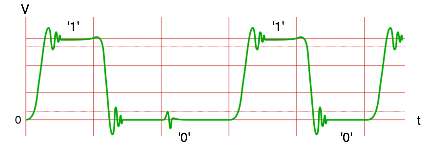
One of the cheapest ways to encode information in terms of 0s and 1s is using voltage levels, illustrated in the diagram below.
Digital Abstraction
The method of determining discrete values out of analog voltage (which value is originally made up of real number, and therefore continuous and infinite) is called the digital abstraction.
This is how digital circuits work. We need to find a reliable framework to determine digital signal values out of analog voltage values. This framework is called the Static Discipline.
What are the benefits of the digital abstraction?
- The digital abstraction is where one interprets voltage values as binary values, thus allowing us to encode information using voltages.
- Using voltages to encode bits of 0’s and 1’s provides a cheap and stable way for us to exchange information through digital devices.
- We can also manipulate or change information encoded using voltages very easily.
The voltages that represent digital bits are generated by semiconductor devices (MOSFET) – something that we will learn in the next chapter. The benefit of using semiconductors the ease of generation, and that they require zero power in steady-state. The drawbacks however, is that the voltages generated by these semiconductors are easily affected by external disturbances, and hence they may be unstable.
To preserve the integrity of information encoded in digital devices made of semiconductor materials, we need to set some contracts between these interconnected digital devices. In this notes, we are going to learn how we can use voltages to encode information in a stable way that follows a particular contract called the static discipline to guarantee the behaviour of each processing block in the system.
A Digital Processing Element: Combinational Device
A digital device is any device that uses voltages to encode information in terms of “low voltage” (bit 0) and “high voltage” (bit 1).
A combinational digital device is a type of digital device where its output is a pure function of the present input only (there’s no memory of past inputs). It is stateless and has the following criteria:
- It requires one or more digital inputs
- It produces One or more digital outputs
- It has a functional specification that details the value of each output for each possible combination of inputs (can be illustrated in terms of truth table / boolean expression)
- It has a timing specifications: propagation delay and contamination delay (later)
You have seen this in our previous chapter: the \(A>B\) 2-bit comparator device is a combinational device, consisted of pure logic gates and behave like a pure function.
Examples include: logic gates (AND, OR, XOR, INV, etc), simple devices like multiplexers, demultiplexers. Later on you will learn another type of digital logic devices called the sequential logic device, whose output depends not only on the present input but also on the history of the inputs, hence having a memory.
Combinational Digital System
A combinational digital system is a larger, more complex digital system made up entirely of combinational circuits.
It has the following criteria:
- Each circuit element is also combinational with no directed cycles (no feedback loop), and
- That very device’s input is connected to exactly one output of another device or to some vast supply of
0s and1s.
Examples include: Arithmetic logic units (ALUs), Control Unit for CPU or memory address decoding.
Voltage to encode information
Combinational devices operate based on logical functions, producing outputs determined solely by current inputs. The inputs and outputs of these devices are represented as binary values (0s and 1s). Binary values are not abstract—they are implemented using voltage levels in hardware.
Voltage is the medium used to encode binary information.
The most naive way to use voltage to encode information is to use ‘low’ voltage to encode valid ‘0’ and ‘high’ voltage to encode valid ‘1’, and define the low and high threshold for each valid ‘0’ and ‘1’.
Anything that is between the low and high threshold value is called the invalid zone because it does not unambiguously represent a binary value. The figure below illustrates a range of low and high voltages accepted by a digital device/system. Out of these voltage values, we can define specific voltage ranges and map them to logic levels.

The values of operating voltage in practice: e.g LVCMOS33 standard is commonly set to be 0.3V for low voltage (binary value 0) and 3.3V for high voltage (binary value 1).
Combinational circuits like AND, OR, and NOT gates rely on these voltage representations to interpret inputs and produce outputs. This encoding must be robust enough to handle noise and imperfections in the physical world.
The Static Discipline
The static discipline is one of the contracts bound for all logical elements making up a digital system.
The Static Discipline
The static discipline is a framework that establishes a contract between digital devices.
The contract: A digital system must be able to produce a valid output (for the next device connected at its output terminal) according to its specification if it is given a valid input.
Purpose: It ensures that circuits are designed to tolerate variations (like noise) and still maintain correct logical behaviour.
Physical implementation: 4 voltage specifications and noise margins to ensure reliable communication between digital devices. These standards define valid voltage ranges for “0” and “1”, and not just single voltage points.
This contract guarantees the behaviour for each processing block in a system, so that a set of such interconnected devices may work properly (are able to pass and compute valid information at the end of the chain of connections). This is necessary so that the system has a predictable behaviour.
A combinational logic device always obeys the static discipline, as it guarantees that the outputs produced will meet the required voltage levels to be correctly interpreted by the next stage of the system, provided the inputs also meet their valid voltage ranges.
However this doesn’t mean that the opposite is true.
A device receiving invalid input does not necessarily produce invalid output. The output from a combinational logic device given invalid input remains unpredictable.
An unconnected terminal or a dangling wire in a digital circuit is not considered a valid low digital signal. In digital electronics, each signal line or terminal must have a definite state: high (1), low (0), or sometimes a high-impedance state.
Voltage Specifications and Noise Margin
A case without noise margin
Consider two digital devices connected in series as shown in the figure below.
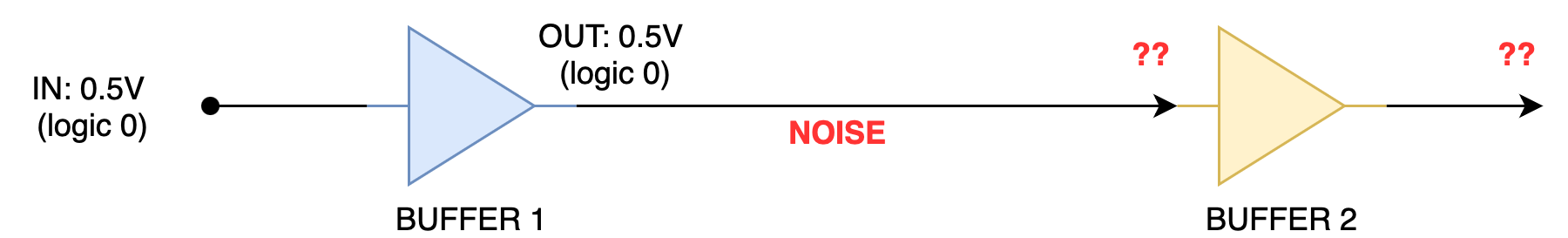
These devices are called a buffer, meaning they pass the same logic level through—if they receive a low voltage, they output a low voltage, and if they receive a high voltage, they output a high voltage.
Buffer
Buffer devices are used to restore signal integrity—even though they don’t alter the logic level (in == out), they help drive stronger signals, isolate circuit stages, and ensure that degraded or noisy signals remain within valid logic ranges.
If we were to naively decide that any voltage below \(V_{low}\)=0.5V as digital bit 0, and any voltage above \(V_{high}\)=2.5V as digital bit 1, then our device may violate the static discipline.
Suppose we supply 0.5V and the first buffer is able to produce also 0.5V as an output, which means digital bit0 .
- Problem: A wire, that connects two or more combinational devices together is susceptible to noise.
- The voltage value that is received at the second 2 may be slightly higher than 0.5V, for example: 0.55V instead, and therefore according to our specification, it is no longer a valid bit
0.
Noise can knock the voltage both up and down because it is a random disturbance caused by factors like electromagnetic interference, power fluctuations, and thermal noise. If noise increases voltage, it might push a 0 into the undefined region or even falsely register as a 1. Conversely, if noise decreases a voltage, it might push a 1 into the undefined region or even falsely register as a 0 under extreme circumstances.
Buffer 1 in the figure would violates the contract because given a valid input, it may be unable to produce a valid output (to reach the next buffer 2), because the 0.5V produced at the output of buffer 1 may meet some disturbances that caused it to be slightly off, e.g: 0.55V.
To ensure noise tolerance and reliable signal transmission, the range for valid output voltages must be narrower than the range for valid input voltages, so that small noise-induced changes do not cause a signal to be misinterpreted as the wrong logic level. This create noise margins that absorb small fluctuations and prevent logic errors.
The 4 Voltage Specifications
We need to account for the presence of some light noise. Instead of naively setting some voltage \(V_{high}\) and \(V_{low}\) as we did above, we need to set a range of Voltages as valid bit 1 and 0 respectively. These ranges of valid voltages gives rise to noise margin, which purpose is to tolerate noise.
Definition
There are 4 voltage specifications: Vol (V output low), Voh (V output high), Vil (V input low), and Vih (V input high) used as a framework to establish static discipline.
It is important that \(V_{ol}\)< \(V_{il}\)< \(V_{ih}\) < \(V_{oh}\). This way, output amplifies the input via regeneration to ensure binary logic levels are maintained reliably across a digital circuit. See appendix for further explanation.
These 4 voltage specifications define the valid voltage ranges for inputs and outputs in a digital system to ensure reliable operation. They define what range of voltage values signifies a valid digital bit
1and a valid digital bit0for ALL combinational logic component in the system.
\(V_{ol}\) (voltage output low) and \(V_{oh}\) (voltage output high) is the voltage that a digital device outputs.
- A voltage value less than \(V_{ol}\) is regarded as digital bit
0 - A voltage value higher than \(V_{oh}\) is regarded as digital bit
1 - The output of a digital system is going to be received by another system after traversing through some wire.
\(V_{il}\) (voltage input low) or \(V_{ih}\) (voltage input high) is the voltage that a digital device receives as input from digital system.
- A voltage value less than \(V_{il}\) is regarded as digital bit
0 - A voltage value higher than \(V_{ih}\) is regarded as digital bit
1
To ensure static discipline, there must be a gap between the output and input specifications, forming the noise margins.
Noise Margin
The noise margin illustrated as the yellow region in the figure below. It adds as a precaution against external disturbances (noise).

The absolute difference between \(V_{ol}\) and \(V_{il}\) is called the low bit noise margin, and the absolute difference between \(V_{oh}\) and \(V_{ih}\) is called the high bit noise margin.
Low-bit/high-bit noise margin is formally defined as the maximum voltage amplitude of extraneous (erroneous) signal that can be added to the noise-free input level without causing a drastic change in the output voltage and that it is still within the valid logic level.
Noise Immunity
The noise immunity (like an “overall” or “effective” noise margin) is the minimum between the high bit noise margin and the low bit noise margin.
Note that the value of \(V_{ol}\) is less than \(V_{il}\), because we would want to have some buffer (margin) against noise. A device always outputs a lower voltage value to signify digital bit 00 and accepts a slightly higher low-voltage value as digital bit 00. The same logic applies for the higher region as well, as \(V_{oh}\) is greater than \(V_{ih}\)
In our previous case earlier, if \(V_{ol}\) is set to be 0.5V, and \(V_{il}\) is set to be 0.6V, then Device 2 will be able to tolerate up to 0.1V of noise (if any). Therefore, 0.55V in our example above is still ‘seen’ as a valid bit 0 when it arrives at the input terminal of Device 2, thus making Device 1 obeys the static discipline.
Once set and chosen, these four voltage specifications: \(V_{ol}\), \(V_{oh}\), \(V_{il}\), and \(V_{ih}\) are to be obeyed by every digital device in an entire combinational logic circuit, e.g: your computer. Think of it like some sort of operating standard across all components in your digital system.
Voltage Transfer Characteristic Function (VTC)
The VTC is a plot between the input voltage (\(V_{in}\)) to a digital system/device vs the output voltage (\(V_{out}\)) of this digital system. It is used to come up with proper values for the 4 voltage specifications in practice, so that these values are well within the physical limitations of the digital device.
- For example, if a device is unable to produce voltage value lower than 0.2V, then we should not set its Vol to be 0.1V
VTC does not tell us how fast the device is. It just captures the static behaviour of the device and tells us what kind of device it is.
The figure below shows the VTC of a buffer: a low \(V_{in}\) gives a low \(V_{out}\) and vice versa.
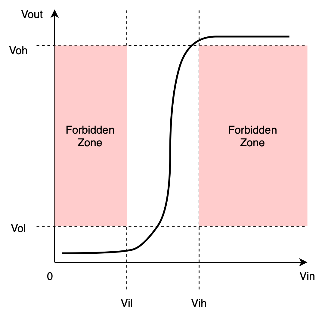
Forbidden zone is not equal to invalid zone. Invalid Zone is the zone where a voltage value does not correspond to digital bit 0 or 1 while Forbidden Zone is the zone whereby static discipline is violated because a valid input voltage does not produce a valid output voltage.
Explanation:
- The red zone is called the forbidden zone. It is formed by the four voltage specifications: \(V_{ol}\), \(V_{oh}\), \(V_{il}\), and \(V_{ih}\) that we set for the entire system.
- The name ‘forbidden zone’ comes from the fact that any value within this zone means that the device receives valid input (less than vil or more than vih) but is unable to produce a valid output hence violating the static discipline and cannot be used as a combinational logic device.
Think!
What will the VTC of an inverter look like?
Purpose of Plotting VTC
The purpose of plotting a VTC (typically obtained from device measurements, i.e: we supply input voltages at intervals and measure the output) is to help us to determine whether or not a digital device can be used as a combinational logic device. We plot the VTC so that we can find a set of four voltage specifications: \(V_{ol}\), \(V_{oh}\), \(V_{il}\), and \(V_{ih}\) for the device so that the device obeys the static discipline.
Semiconductor engineers and circuit designers (from large manufacturers) typically does this work during manufacturing process. They determine the four voltage specification and plot VTCs from various transistor types primarily to design and manufacture logic gates and digital ICs. Small manufacturers typically don’t do this and rely on pre-defined specs from transistor manufacturers.
As a digital circuit engineer, your steps would be:
- Prototype & Characterize: Purchase sample transistors from different manufacturers, build test circuits, and measure their VTC to evaluate their real-world performance.
- Analyze & Define Specs: Compare the measured VTC against proposed digital logic voltage levels (Vol, Vil, Vih, Voh) and noise margins, tweak these proposals if necessary depending on constraints (cost, size, temperature) and selecting the best-performing components.
- Mass Production: Once the chosen transistors meet the system’s static discipline requirements, bulk order them for large-scale manufacturing and integration.
Real Life Example
All commercially available combinational digital devices (logic gate ICs, multiplexers, decoders, etc.) have their voltage specifications clearly documented in their datasheets.
For example, the following device is called the 74HC32 Quad 2-Input OR Gate:
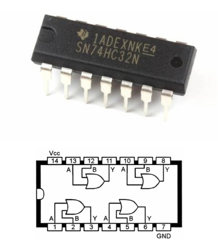
Its datasheet reports the four voltage specs under various conditions (different temps, different voltage source level). Note how the relationship between the voltages is Vol < Vil < Vih < Voh in all conditions.
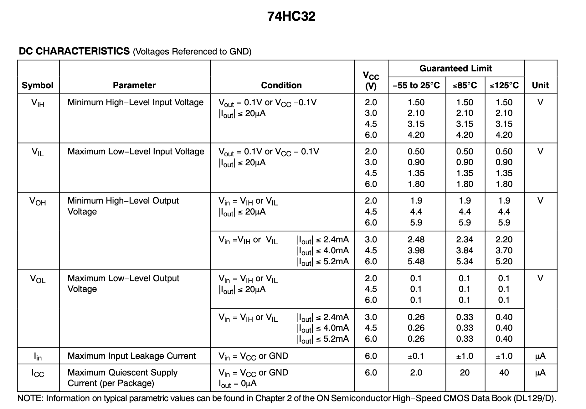
Full specs can be found here.
These 4 voltage specs are always reported in datasheets of digital logic ICs because they define compatibility between logic devices, ensuring reliable signal transmission and correct logic interpretation. Without these specs, designers couldn’t guarantee proper operation, noise margins, or interoperability in digital circuits.
Determining if a digital device can be used as a combinational logic device
You can quickly tell if a digital device can be potentially be used as a combinational logic device iff: you can find a set of these four voltage specifications: \(V_{ol}\), \(V_{oh}\), \(V_{il}\), and \(V_{ih}\) whereby its VTC curve does not cross the forbidden zone and that \(V_{ol}\)< \(V_{il}\) < \(V_{ih}\) < \(V_{oh}\).
Steps:
- We typically begin by setting \(V_{ol}\) and \(V_{oh}\) first which are typically set by the technology standards of the logic family (e.g., TTL, CMOS).
- These ensure that the circuit produces reliable logic levels before worrying about how inputs interpret them
- Then, we can propose \(V_{il}\), and \(V_{ih}\), and check if the curve crosses the forbidden zone (check if static discipline obeyed) formed by these four values.
- If static discipline is violated, we either adjust our guess or find another device.
Goal: we want to choose \(V_{ol}\), \(V_{oh}\), \(V_{il}\), and \(V_{ih}\) that maximises noise immunity.
VTC Characteristics of a Combinational Logic Device
The VTC curve of a combinational logic device must possess both characteristics below:
-
There exist some region in the VTC whereby its absolute
\[\begin{aligned} \text{Gain}(V_{in}) = \frac{d V_{out}}{d V_{in}} \end{aligned}\]Gainis \(>1\) .Gainis actually a function of \(V_{in}\) and is formally defined as:In layman terms you can approximate
\[\text{Gain} \approx \frac{V_{out_l}-V_{out_k}}{V_{in_j}-V_{in_i}}\]Gainduring some transition \(V_{in_i}\) to \(V_{in_j}\) that results in some \(V_{out_k}\) to \(V_{out_l}\) respectively by the simply computing the slope between these two points on the VTC:If you have found four voltage specifications \(V_{ol}\), \(V_{oh}\), \(V_{il}\), and \(V_{ih}\) for which the device still obeys the static discipline, you can approximate device’s maximum
\[\max\text{Gain}\approx \frac{V_{oh} - V_{ol}}{ V_{ih} - V_{il}}\]Gainby computing:If absolute
Gain\(>1\), then there is a finite, positive noise margin. If absoluteGain\(=1\), then there’s zero noise margin. It is impossible to have absoluteGain\(<1\) and still have the four Voltage specifications \(V_{ol}\) < \(V_{il}\) < \(V_{ih}\) < \(V_{oh}\). Also, having absoluteGain > 1maintains integrity of the signal passed through the system as signal loss is inevitable in the real world. -
The device has a Non-linear
Gain, meaning thatGainis a function ofVinand therefore the gradient along the entire curve varies.- The VTC curve for a combinational logic device should not be entirely made of a single, constant gradient like the shape of a plot from a basic line equation, but rather more towards an “S” (or mirrored S) shape.
If both characteristics above aren’t satisfied in the VTC curve, then it is not the VTC of a combinational logic device.
Summary
You may want to watch the post lecture videos here.
Here are the key points from this notes:
- Static Discipline: An important contract (via setting the four voltage specifications), to ensure that the output of a digital component behaves correctly given specific valid input levels. This contract governs all digital devices in a system (not just a single gate!)
- Noise Margin and Noise Immunity: We need to take into account the presence of noise when we establish the voltage specification contract, so that we can still obey the static discipline despite the presence of noise.
- VTC Graph: A plot describing the behaviour (Vout vs Vin) of a digital device. This is very useful to determine reasonable voltage specifications that obey the static discipline. We need to ensure that the graph does not cross the forbidden zone.
Smaller logic gates can be assembled to form more complex units and ultimately entire computer systems. We can be confident that the computer system will work predictably by ensuring that each sub-component obey the static discipline. This layered approach not only simplifies the design and development of digital devices but also ensures that even small components adhere to necessary standards to function correctly within the larger system.
Next Steps
In the next chapter, we will learn about the MOSFET (transistor), that is one of the smallest component (building block) that makes up a digital device, and how we can use them to form a proper combinational logic elements we call gates. These gates can be used to form an even larger combinational circuits such as the adder, shifter, etc, and an even larger one such as the Arithmetic Logic Unit (you will build them in Lab 2 and 3).
Each larger device will provide greater level of abstraction:
- At first we have MOSFETs (transistors) that we can use to make logic gates. Once we are using logic gates, we abstract away the details about our transistors.
- We can then use logic gates to make more complex logic units like ROMs, microcontrollers, multiplexers, registers, and CPU. Realise that once we have a CPU, we abstract away the details about our little logic gates.
- Once we have a CPU, we can create an assembler to help us program an operating system in assembly. We can create more useful programs like compilers to help us create programs easily in higher level language. This is how abstraction works: we create smaller components and use them together so that we can do our job (as programmers) easily.
Therefore, it is imperative that each combinational logic device / component, no matter how small, must conform to the static discipline and the established four voltage specifications (that must be chosen such that it fits with their VTC) so that the larger system can work as intended.
Appendix
In digital systems, the term “output amplifies input” refers to the restoration or regeneration of signal levels by digital gates or devices to maintain distinct and reliable binary states.
Maintain signal integrity across stages
As signals propagate through circuits, they experience degradation due to resistive losses (voltage drops in wires), capacitive effects (slower transitions), and noise accumulation (fluctuations from the environment). Without amplification, these effects accumulate, causing the signal to drift into the invalid zone or become indistinguishable. A gain greater than 1 ensures that outputs regenerate the input to valid logic levels (Vol or Voh), restoring signal integrity for subsequent stages.
How Output Amplifies Input
In digital logic gates, the transfer function ensures that small changes in input voltages near Vil or Vih result in large changes in output voltages, driving them to valid levels Vol for 0 or Voh for 1. A steep transfer function slope (gain > 1) allows the output to “snap” to valid states, effectively amplifying and stabilizing the input signal.
Without Amplification (Gain ≤ 1)
If the gain is 1, the input-output relationship becomes linear, propagating noise directly without restoring valid levels. For gain < 1, signals weaken further, violating voltage specifications (Vol < Vil < Vih < Voh) and causing signals to degrade beyond recovery, making the system unreliable.
In short, amplification restores signal levels to ensure valid logic outputs, counteracting signal loss caused by noise and degradation. It enforces static discipline, guaranteeing that valid inputs produce valid outputs, and prevents cascading errors by regenerating distinct binary levels across multiple circuit stages.
The amplification is not “amplification” in the analog sense (where signals are continuously increased), but rather the regeneration of signals to ensure binary logic levels are maintained reliably across a digital circuit. Without this, digital systems would quickly fail due to noise and signal loss.