 50.002 CS
- Overview
- Storage Device: D-Latch
- Proposed Solution
- DFF as Memory Device
- D Flip-Flop Timing Constraint
- Sequential Logic Device Timing Constraint (t1 and t2)
- \(t_{pd}\) and \(t_{cd}\) of Sequential Logic vs Combinational Logic Devices
- Synchronization with Input
- The Metastable State
- Summary
- Appendix
50.002 Computation Structures
Information Systems Technology and Design
Singapore University of Technology and Design
Sequential Logic and Synchronization
You can find the lecture video here. You can also click on each header to bring you to the section of the video covering the subtopic.
Detailed Learning Objectives
- Distinguish Sequential and Combinational Logic Devices
- Explain the functional differences between sequential and combinational logic devices.
- Explain the role of memory elements in sequential devices which allow them to store and reference past inputs.
- Explain Memory Devices: D Flip-Flops and D-Latches
- Discover the structure and operational modes (write and memory modes) of D Flip-Flops and D-Latches.
- Examine how these memory devices integrate with combinational logic to form sequential logic circuits.
- Identify the Role of the Clock Signal
- Justify the critical role of the clock (CLK) signal in managing the behavior of sequential logic devices.
- Explain how the CLK signal ensures synchronization of inputs for reliable operation.
- Discuss Edge-Triggered D Flip-Flops
- Discuss the design and functionalities of Edge-Triggered D Flip-Flops, focusing on master and slave latch configurations.
- Assess the importance of clock signal inversion and its impact on the operational dynamics of D Flip-Flops.
- Justify Dynamic Discipline Requirements
- Explain the necessity of setup time and hold time to prevent the storage of invalid information.
- Explain how adhering to dynamic discipline ensures the reliability of sequential circuits.
- Analyze Timing Constraints in Sequential Circuits
- Explain the importance of critical timing constraints
t1andt2between sequential logic devices.- Prove how
t1andt2constraints ensure stable and valid outputs throughout clock cycles.- Discuss Synchronization Challenges of External Inputs
- Explain the difficulties in synchronizing external inputs with the clock in sequential circuits.
- Examine potential issues arising from violations of the dynamic discipline.
- Explain the Metastable State in Sequential Logic Devices
- Identify what a metastable state is and the conditions that lead to its occurrence in sequential logic devices.
- Evaluate the consequences and impacts on circuit functionality when a device enters a metastable state.
- Evaluate Methods to Minimize Metastability
- Analyze strategies to reduce the likelihood of a device entering a metastable state.
- Measure the trade-offs involved in these strategies, such as cost, responsiveness, and device size.
The aim of these learning objectives is to thoroughly understand sequential and combinational logic devices, focusing on their differences, integration of memory elements, operational synchronization, and challenges in maintaining reliable and efficient functionality.
Overview
We’ve covered the basics of combinational logic devices, which produce outputs based solely on current inputs and must adhere to specified truth tables. However, external inputs are unreliable and may not persist long enough for the device to process them effectively. To manage this, we need methods to synchronize input signals to ensure sufficient processing time.
Additionally, we need to explore sequential logic devices, which depend on both current and past inputs. Known as finite state machines (FSMs) when they have a limited number of states, these devices incorporate memory to store and reference past inputs. Further details on FSMs will be discussed in the next chapter.
Recap
A simple combinational logic device does not remember its output value. It only gives an output when there’s an input, and the output(s) stay(s) stable for as long as its input(s) is/are stable. A memory device on the other hand, is a device of which we can write new values to and is able to remember this value for a period of time.
We can connect memory device(s) together with combinational logic device(s) to form a sequential logic device. Notice the presence of a CLK signal below. A sequential logic device has a general structure as shown below:

In the next few sections we will learn how to create this memory device labeled as Registers above (or more specifically, it is called D Flip-Flop).
Storage Device: D-Latch
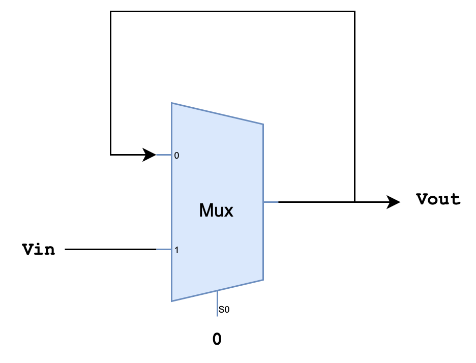
A D Flip-Flop (memory device) is made using another device called a D-latch. A D-latch can be created using a multiplexer with a feedback loop,

This is not the only way to make a D-latch. A simple Google search will present you with some other alternatives. We just use a multiplexer here to explain the idea easily.
How it works:
- In practice, G is clock (CLK) signal. It will periodically switch between
1s and0s (valid high voltage and valid low voltage) as shown in the image below:

- Q is the output of the latch, and D is the (external) input that’s placed at the second input port the latch.
- Q is fed back as Q’, the first input port of the latch.
- If G is 1, then the input signal on wire D will be “passed” to / reflected at output wire Q, independent of the signal on wire Q’.
- Lets call this the
writemode.
- Lets call this the
The term “pass through” is used from this point onwards in this chapter to easily explain the behavior of the MUX, that when G=1, then value at Q always reflects the value at D. However recall from from Week 1 lecture (CMOS) that the signal at Q is actually due to the VDD or GND and D is simply the input at the gate that activates or deactivates the pull-up or pull-down components of the latch.
- If G is 0, then output signal on wire Q reflects the signal on wire Q’, independent of input wire D.
- Lets call this the
memorymode (orreadmode in some textbooks).
- Lets call this the
Before we progress, let’s ensure we understand one thing first:
- The theory of a working D latch is that when G transitions from HIGH to LOW, Q should hold the value present on D at that moment.
- However, a combinational device (the Mux) makes NO output guarantees until \(t_{pd}\) after an input change and may behave unpredictably between \(t_{cd}\) and \(t_{pd}\).
- This is time gap between “remembering old stable value” to “producing new stable value” as input transitions.
So if the falling edge of G briefly invalidates Q, the memory fails because Q is exactly what we are trying to preserve. Therefore, we must ensure that a HIGH-to-LOW transition on G does not disturb Q at all. This is done by the hardware, which is to build a lenient MUX. You can read the appendix section if you’re interested, but as long as you can take at face value that HIGH TO LOW transition on G does not disturb Q at all, as long as some prerequisites about D holds (will be explained below), then you’re good to continue.
Using a D-Latch
A D-latch operates by capturing the input voltage (valid low or high) at the D wire when a valid high voltage is applied to the G wire (also shown as the Clock port in the diagram below). After the voltage at G switches to low, the D-latch retains the value from D at the time G was high, without needing to maintain D’s initial values.
By arranging multiple D-latches in parallel, we can create a stable N-bit output that “remembers” the input values without requiring continuous input at the D ports. This stored output can then serve as a reliable input to a combinational logic device for the duration of its processing time (\(t_{pd}\)), mitigating issues with unreliable external inputs.
The accompanying figure demonstrates a setup with a 4-bit input and a corresponding 4-bit output. Each rectangle (marked with a “>” at its lower left corner) represents a Flip-Flop, which consists of D-latches and will be discussed in a later section.

From this point onwards, 1 simply means valid high voltage, and 0 means valid low voltage .
Problems
There are two problems that arises from using this simple D-latch in our electronic devices without any contract / rules:
1: Storage of invalid information
If G changes from 1 to 0 at the exact moment when D just turned invalid from previously being valid, then we might end up storing that invalid value of D when the latch enters memory mode.
2: Invalid/unstable output due to transition in input
If the existing stable input value in D is flipped, e.g: is changed from 1 to 0 or vice versa, the value at D will be invalid (momentarily) during this transition.
The voltage value at D can also be invalid (unstable, unreliable) due to any disturbance. This will affect the output at Q if G is 1, because it will pass all input from D to the output wire Q, regardless of whether it is a valid or stable input or not (during transition or any disturbance). We end up with potentially unstable/invalid output half the time.
In practice, this is not acceptable because we do not want our electronic devices (e.g: computers) to have invalid output computed (e.g: be unstable, or hang, or freeze) at any point in time, even when D is transitioning. We want it to be robust, and reliable at all times.
Combinational component within an electronic device requires a certain amount of time tpd to produce meaningful results; and over this time-frame we need to hold its input stable, however external input is unreliable, so there’s no guarantee that this requirement is fulfilled.
Proposed Solution
As a solution to this problem we create another device using D-latches called D Flip-Flop (DFF) or more informally a Register to synchronize external input with the circuit’s CLK, and also switch between write and memory mode as we intend it to behave.
A D Flip-Flop with a right Clock setup will be able to produce a valid and stable output for an entire clock period; long enough for any combinational logic connected downstream to finish its computation (\(t_{pd}\)) and produce meaningful output before the next output value is produced.
We address these problems in the next two sections.
The Dynamic Discipline
The dynamic discipline is a contract that is made to address the first problem above: the possibility of storing invalid information in the memory device. It is imperative to never violate the dynamic discipline to ensure any sequential logic circuits to work properly.
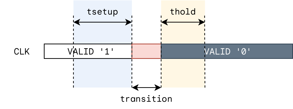
The dynamic discipline states that there are two timing requirements for the input signal supplied at D, named as \(T_{setup}\) and \(T_{hold}\):
- \(T_{setup}\) is defined as the minimum amount of time that the voltage on wire D needs to be valid/stable BEFORE the clock edge changes from
1to0(turning fromwritemode tomemorymode). - \(T_{hold}\) is defined as the minimum amount of time that the voltage on wire D needs to be valid/stable AFTER the clock edge reaches a valid
0from a previous1.
These two values are crucial for later.
\(T_{setup}\) and \(T_{hold}\) are not contiguous. \(T_{setup}\) ends when G begins transitioning from
1toward0, and \(T_{hold}\) begins only when G reaches a valid0. The clock’s own finite transition period sits between them: neither \(T_{setup}\) nor \(T_{hold}\) formally governs D during this interval.
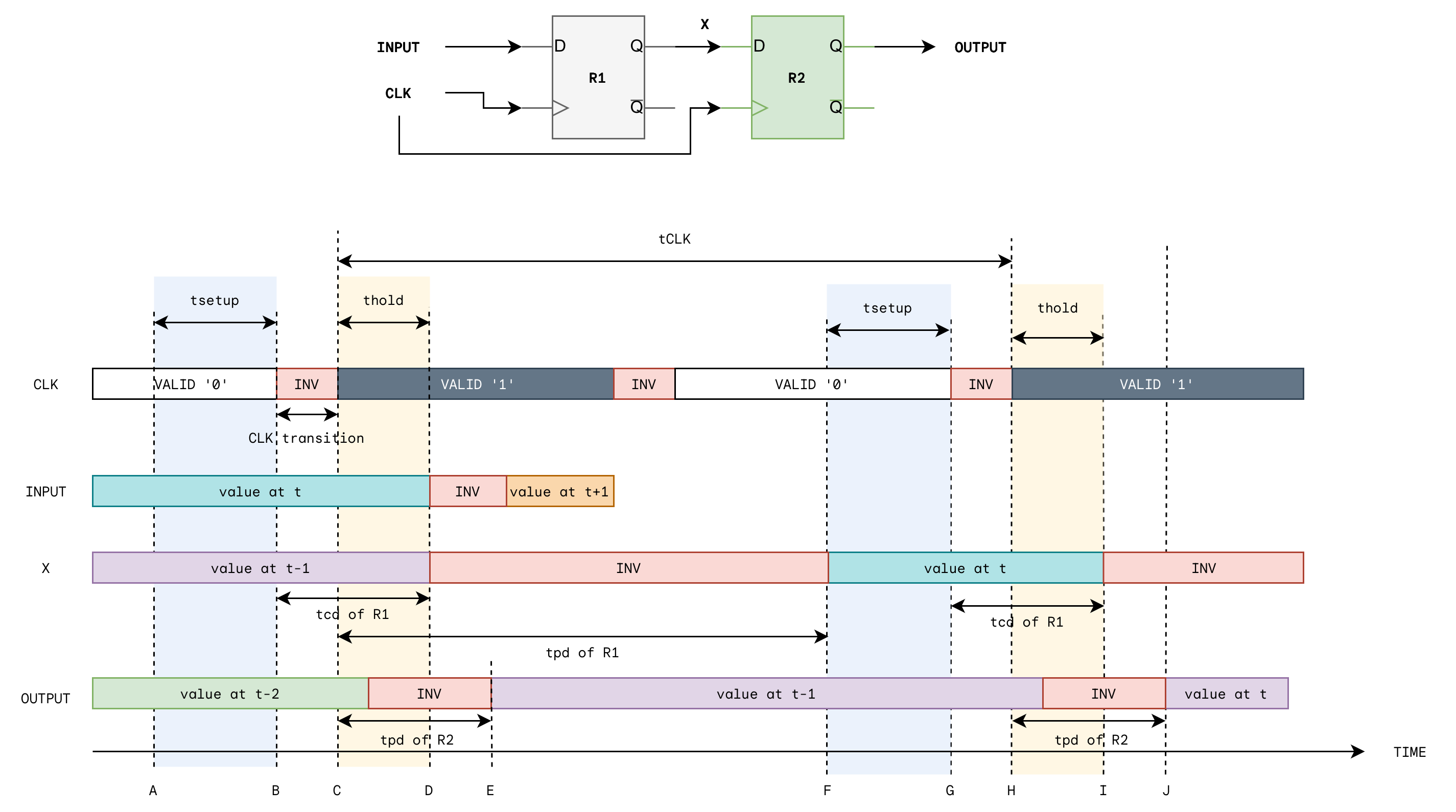
Edge-Triggered D Flip-Flop
To address the second problem: the presence of unstable/invalid output during transition of input, we need to create another device called the Edge-Triggered D Flip Flop (or shortened as DFF) by putting two D-Latches in series as shown:

At first, each of the two rectangles are the symbol of a regular D-latch. Putting them in series (and inverting the CLK signal fed to the first latch) results in a DFF (the rectangular symbol on the right). The difference is that in a DFF, the CLK input port is represented by the > symbol at its lower left corner.
General Anatomy
We can describe the structure of a Flip-Flop as follows:
- The first D-latch that receives the external input D is called the MASTER latch, and the second D-latch is called the SLAVE latch.
- There is an inverter applied on the G input on the master Flip-Flop, so the master latch receives or “sees” the inverted clock signal.
- The star (\(\star\)) symbol represents the intermediary output and its not observable outside of the system.
- The output at the Q port of the slave latch is the observable output of the Flip-Flop.
The Beauty of DFF
How does a Flip-Flop prevent the presence of invalid/unstable output during transition/disturbance of input at D?
The observer/user gets output only from the output wire of the slave latch’s Q port, and the observer/user supplies input only to the master latch’s D port.
Notice that CLK is a signal that periodically changes from 0 to 1 and vice versa.
When CLK signal is 0, the G port of master latch will receive a 1 (due to the inverter) and the G port of slave flip flop will receive a 0 at the same time.
- This means that the master latch is in “
writemode”, i.e: it lets signal from its D wire through to its Q port, while the slave latch is in “memorymode”, i.e: slave’s output depends on its own memory Q’ and not affected by input on \(\star\).
When CLK signal is 1, the G port of master latch will receive a 0 due to the inverter and the G wire of slave latch will receive a 1.
- This means that the master latch is in “
memorymode”, i.e: master’s output depends on its own memory Q’ and is not affected by any value on input port D. - Meanwhile, the slave latch is on “
writemode”, i.e: it lets signal from the \(\star\) wire to be passed through its slave input port D.
Hence, only ONE of the two D-Latches is on “write mode” at a time or equivalently, only one D-latch is on “memory mode” at a time. Unlike a single D-latch alone, this Flip-Flop configuration prevents a direct reflection of the input of the system (supplied by the user) to the output of the system.
The explanation above is illustrated in terms of waveforms below. Take some time to study the waveforms and convince yourselves that they make sense. Note that “Q” here means the overall output of the Flip-Flop, which is the signal produced by the Q port of the slave latch.

Notice two further behaviors in the Flip-Flop:
- Unlike the \(\star\), the signal at Q is stable throughout an entire clock period, and change only in the next clock period. In comparison, the \(\star\) is only stable half the time when the master latch is at
memorymode, but reflects ever-changing D-input signal duringwritemode. - The edge-triggered flip-flop in this particular configuration, where the master is the one that receives the inverted CLK signal produces new value at Q (reflects the input at D) at every rising edge of the CLK.
It is as if we are able to capture the instantaneous value of D at each CLK-rise edge (like a camera shutter), and produce it at Q (stable) for that entire period of the CLK.
You can also make the slave latch to be the one that receives the inverted CLK signal, and the value at Q reflects the input at D at each falling edge of the CLK. The name “edge-triggered” comes from the fact that the output at port Q of the slave changes only when the CLK edge changes (in our case, at every rising edge).
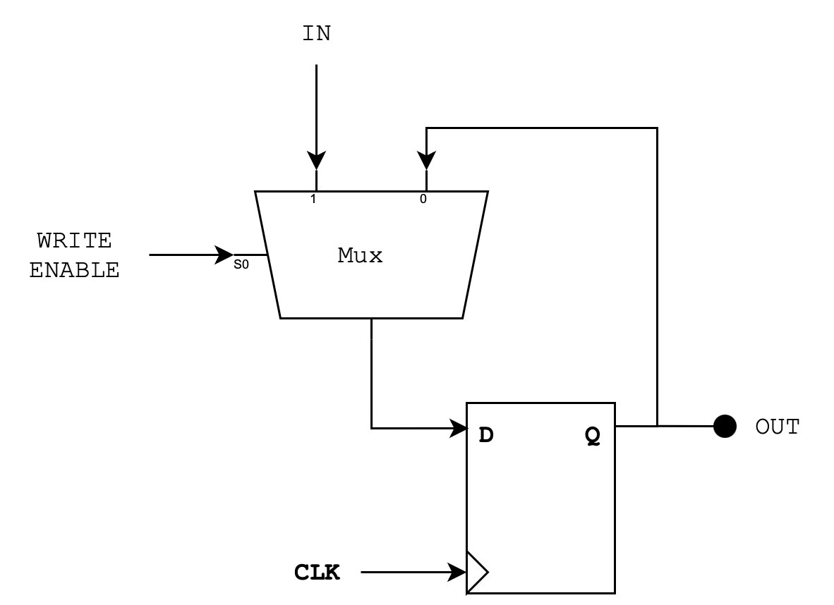
DFF as Memory Device
A DFF always outputs a stable and valid value at its Q port for one clock period (regardless of the actual input at the D port), before changing it to a new updated value. In a way, it is able to memorise whatever value at D was during CLK rising edge for an entire CLK period thereafter.
We can create another circuit using a DFF to allow it to either always output a previously stored value regardless of the CLK, or to load a new IN value into the DFF when needed using a control signal called WRITE ENABLE.
A simplified anatomy is shown below:
You will meet this device later on .
D Flip-Flop Timing Constraint
Recall that the dynamic discipline (\(T_{setup}\) and \(T_{hold}\)) ensure that we do not end up storing invalid input signals. In the flip-flop configuration, we connect two D-latches together. Hence the dynamic discipline for the slave latch has to be obeyed by the master latch because the output of the master latch is the input to the slave latch.
To obey the dynamic discipline, there exist this timing constraint for the D Flip-Flop configuration:
\[t_{CD_{master}} \geq t_{H_{slave}}\]Head to Appendix if you’re interested to learn why.
Sequential Logic Device Timing Constraint (t1 and t2)
We can integrate Flip-Flops into our circuits as ‘synchronization’ or ‘memory’ devices, ensuring stable output for at least one clock cycle. These can be placed either before or after any combinational logic circuit. To ensure reliable operation of such sequential logic circuits or devices, adherence to the dynamic discipline is crucial at all times. This discipline ensures that all parts of the circuit properly manage timing, charge, and signal integrity to function correctly.
Due to Dynamic Discipline, we have two timing constraints called \(t_1\) and \(t_2\) that should always apply in ANY path between two (one upstream and one downstream) connecting Flip-Flops (regardless of how many CLs are there in the middle of the two Flip-Flops) in a SL circuit.
Take into example a very simple circuit as shown in the figure below, consisted of two Flip-Flops and one CL device in between. Let’s name the Flip-Flop R1 on the left as the “upstream” Flip-Flop and the Flip-Flop R2 on the right as the “downstream” Flip-Flop:
Each of these are a DFF! Not slave-master latch setup.
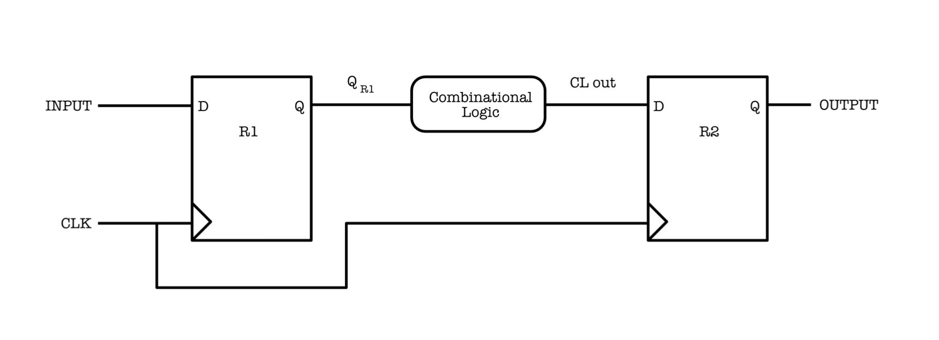
If we were to plot the timing diagram of the CLK, output of R1 (\(Q_{R1}\)), and the output of the CL (CL out), we have the following:

From the diagram above, we can define two timing constraints for this particular scenario where \(t_{CLK}\) is the CLK (clock) period.
- \(t_1\) : \(t_{CD} R_1 + t_{CD} CL \geq t_{H} R_2\)
- \(t_2\) : \(t_{PD} R_1 + t_{PD} CL + t_S R_2 \leq t_{CLK}\)
These formulas assume the clock signal transitions instantaneously: a standard idealization used throughout this course. In reality, every clock edge has a finite transition time \(t_{slope}\), which introduces reference-point mismatches between the timing quantities above. For \(t_1\) this mismatch is self-correcting; for \(t_2\) it introduces an explicit \(t_{slope}\) term. See the appendix for further explanation (not required in the syllabus).
You may read this supplementary document to know more about timing computations for sequential logic device. If you’re interested to find the reasoning behind t1 and t2 constraints, read this appendix section.
\(t_{pd}\) and \(t_{cd}\) of Sequential Logic vs Combinational Logic Devices
In the previous chapter, we learned about the definition \(t_{CD}\) and \(t_{PD}\) for combinational logic (CL) devices, and how to compute these values. For sequential logic (SL) devices, i.e: circuits with Flip-Flops and CLs combined, these timings mean as follows:
- \(t_{CD}\) of a Flip-Flop (or sequential logic devices) is the time taken for an invalid CLK input (not input to the sequential logic circuit), as a result of transition from
0to1, to produce an invalid final output of the SL (Sequential Logic) device. - \(t_{PD}\) of a Flip-Flop (or sequential logic devices) is the time taken for valid
1CLK input (again, not input to the sequential logic circuit), to produce a valid final output of the SL device.
Subtle Difference
In combinational devices, there is no input CLK and units with feedback paths like the Flip Flops involved. \(t_{PD}\) of a combinational device is the time measured from the moment a valid input is fed to the circuit to the moment it produces a valid output of the circuit, and \(t_{CD}\) is the time measured from the moment an invalid input is fed to the circuit to the moment it produces an invalid output.
However in sequential logic devices, our input will be the CLK and not the “user” input, and in particular only are concerned with the CLK transition from 0 to 1, where the D Flip-Flop “captures” a new input value.
Synchronization with Input
In any sequential logic circuit we use a single synchronous clock, meaning that we use one same clock to any D Flip-Flop in the device. Our timing constraints ensure that the CLs are given valid and stable input long enough for it to produce meaningful output. However, we still have one small issue: the external input need to obey the dynamic discipline for the first ‘upstream’ DFF (that directly receives external input) in the circuit.
Why is this an issue?
In practice, it is not possible for any arbitrary input to always be synchronised with the clock, i.e: to obey the \(t_S\) and \(t_H\) requirements (of the external input facing ‘upstream’ DFF) at all times. For instance, when you type on your keyboard, you aren’t able to synchronise that keyboard presses with your CPU clock, are you?
Violating the Dynamic Discipline
Recall that dynamic discipline is crucial for any sequential logic circuit to work properly. We are now going to investigate what happens if dynamic discipline is violated. In the figure below, suppose tH constraint is violated and the D latch captures an invalid voltage range:
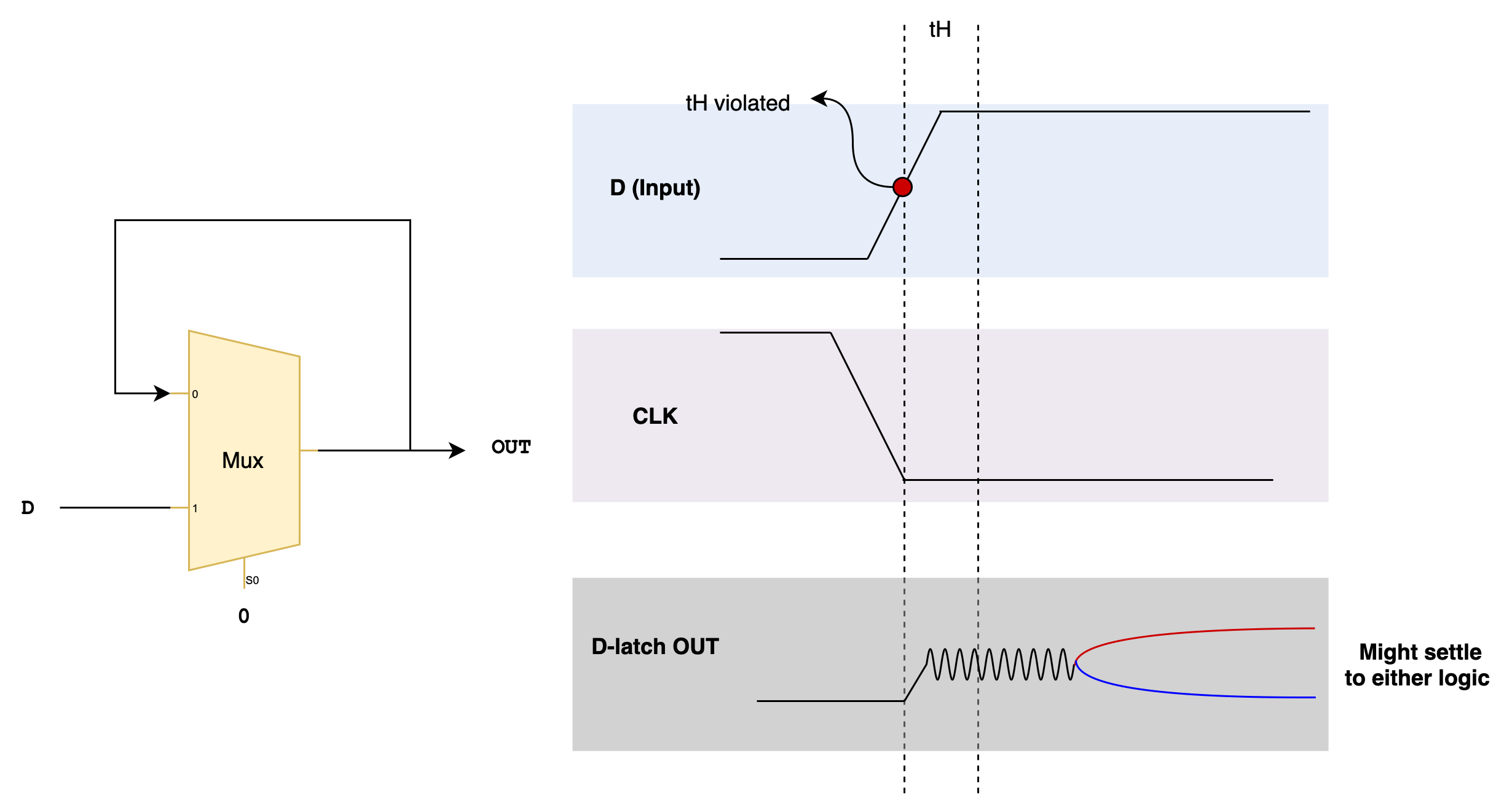
We may end up storing the invalid values during memory mode (CLK is 0) instead of a stable 0 or 1. This condition is what we refer to as the metastable state, where the output is undefined (does not correspond to any valid logic value) and could lead to unpredictable behavior in the system. This is because:
- The output might resolve to either
0or1after an unpredictable delay, meaning different runs on the same circuit could produce different results (non deterministic) - This gets worse in downstream components: If multiple downstream gates receive the metastable signal, some might interpret it as 0 while others as 1, leading to inconsistent logic states and system instability.
- Glitches: If an intermediate or fluctuating voltage is fed into a gate, different transistors inside the gate may interpret it differently, leading to a glitch—a brief, unintended transition in the output. This will affect timing constraints of even more device downstream.
The Metastable State
The metastable state
When the dynamic discipline (t1 and t2 time constraints) is violated, the dff may enter a metastable state, meaning its output is neither a stable 0 nor a stable 1 for an unpredictable duration. The output might still resolve to a valid 0 or 1, but the resolution time is uncertain, and this makes it dangerous.
As mentioned above, if the resolution takes too long, it can violate timing constraints in downstream logic, leading to incorrect or unpredictable behavior.
If metastability propagates, different parts of the circuit might interpret the unstable signal differently, causing divergent outputs and system failures.
Cause
Due to the existence of a feedback loop in the D-latch as shown, it has a unique property where there exist a point in its voltage characteristics function whereby \(V_{in} = V_{out}\).
The VTC plot of the D-latch setup above is as follows:
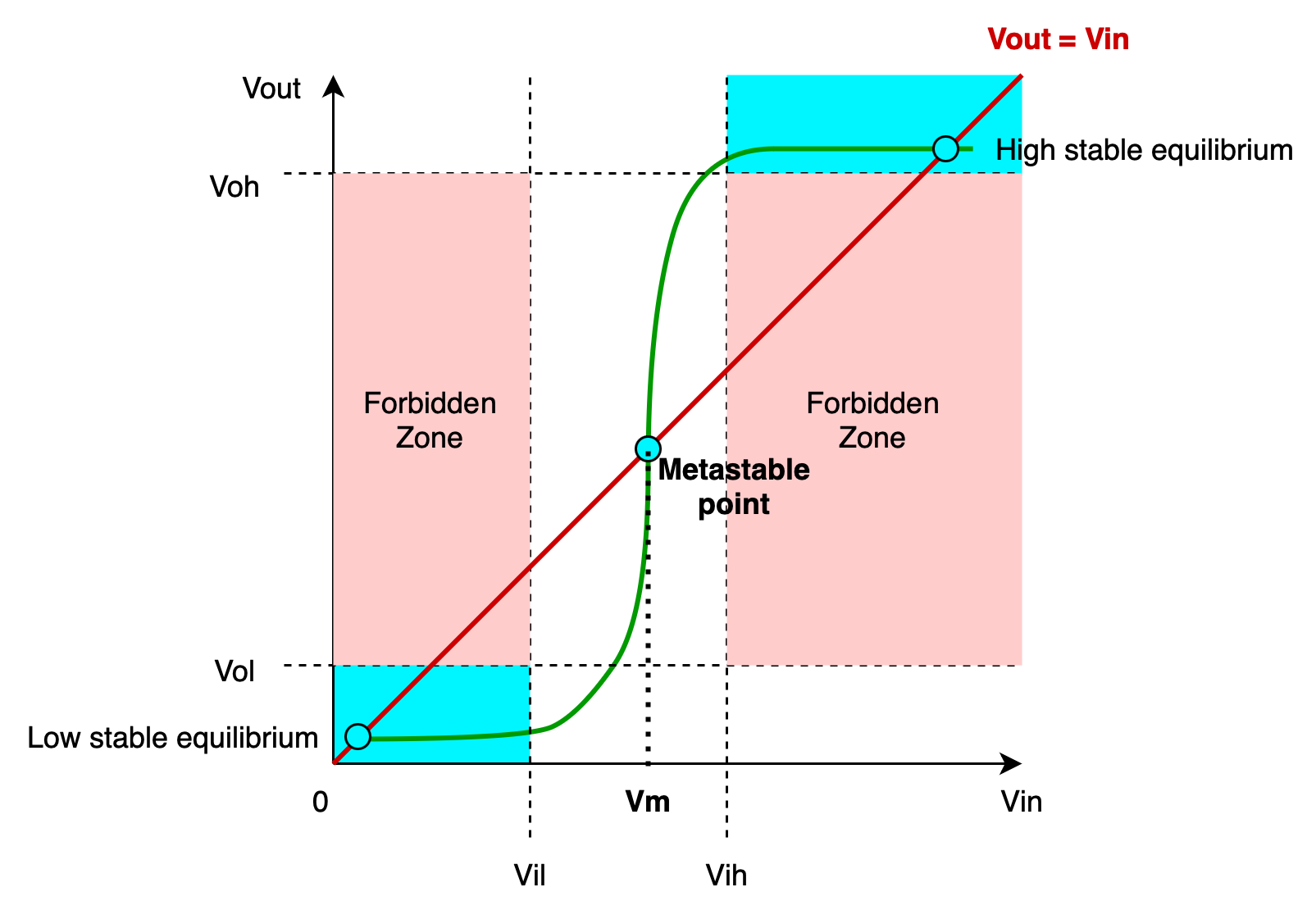
The red line signifies the feedback constraint, where we have Q at \(V_{out}\) to be equivalent to Q’ as \(V_{in}\). This is the effect of the feedback loop.
The green line signifies the VTC of a “closed latch” state, i.e: when the selector bit of the multiplexer receives a 0 as shown in the diagram above.
In the memory mode (closed-latch state), the D-latch passes the value from \(V_{in}\) (Q’) as the output at \(V_{out}\) (Q), and thus we have a shape that resembles that of a buffer.
There are three points formed by the intersections of the red line (feedback constraint) and the green line (VTC of the closed latch), as indicated by the three circles in the figure above:
- Two end points that results in “valid” voltages (either
0or1). These are called low and high stable point. - One middle point that called the METASTABLE point
- The \(V_{in}\) value at this point is denoted as \(V_m\)
What is the significance (meaning) of these solution points?
The stable equilibrium points (high and low) are where the D-latch naturally settles, corresponding to the stored logic
1and logic0states. The metastable point is an unstable equilibrium where the system momentarily balances but will eventually resolve to one of the stable states due to noise or small perturbations.
Thought Experiments
Let’s think about a few scenarios while looking at the VTC plot above.
1: Initial \(V_{in}\) value is well below \(V_m\).
This will land the output voltage at the low stable equilibrium region.
- With initial \(V_{in}\) value « \(V_m\), the device will produce a lower \(V_{out}\)
- This \(V_{out}\) will loop back as \(V_{in}\), and produce an even lower value of \(V_{out}\) at the next iteration
- Eventually, the value of \(V_{out_N}\) after certain N loops traversal tends towards the stable low equilibrium point
2: Initial value of \(V_{in}\) is well above \(V_m\)
This will land the output voltage at the high stable equilibrium region.
- Conversely,with initial \(V_{in}\) value » \(V_m\), the device will produce a higher \(V_{out}\)
- As this \(V_{out}\) loops back and becomes a new \(V_{in}\), it will produce an even higher value of \(V_{out}\) at the next iteration
- Since \(V_{out_i}\) is always greater than \(V_{in_i}\) at each loop \(i\), we will eventually have a \(V_{out}\) value that tends towards the stable high equilibrium point
3: Initial value of \(V_{in}\) is equal or near to \(V_m\)
We are at the metastable point.
- If we have \(V_{in} = V_m\) (exactly at \(V_m\)), then its \(V_{out}\) will be near \(V_m\) again.
- Under noise-free condition, \(V_{out}\) will always be equal to \(V_{in}\) no matter how many times the signal loops (no improvement!)
- We might indefinitely be stuck at this metastable point (invalid voltage value)
Why is invalid logic value a problem?
If an upstream component propagates an invalid (metastable) voltage, downstream logic gates may interpret it inconsistently, leading to unpredictable or divergent outputs. This can cause timing violations, glitches, or delayed resolution, potentially corrupting data or causing system instability.
Unpredictable output: Digital devices receiving invalid voltage input value may produce either
0or1randomly, meaning that different executions of the same operation may yield different results, making the system unreliableDivergent output: If multiple downstream gates receive an invalid signal (metastable), some gates might interpret it as
0(settled to0) while others interpret it as1(settled to1), causing different parts of the circuit to operate on conflicting logic states, leading to glitches, race conditions, or system instability
Noise is Good, Sometimes
Without the presence of noise or external disturbances, if \(V_{in}\) is exactly at \(V_m\) then there is always a chance that we MIGHT wait forever for it to be able to settle to either a stable values. A small presence of noise will drive \(V_{in}\) down or up and eventually it may settle to a stable value, however this is not guaranteed in bounded time.
If we wait for a metastable value to settle, it may resolve to the wrong state (not necessarily the original input), but this is still preferable to remaining in an undefined state indefinitely. Digital systems require a definite
0or1to ensure predictable operation, even if the resolved state doesn’t always match the original input.The actual true value of the input is effectively lost (when it violates the dynamic discipline that caused this metastable state for example).
Properties of Metastable State
The state whereby your SL device is unable to settle to a stable valid value for unknown period of time is called the metastable state. Obviously we do not want this because the output of the device is invalid during this unknown time frame, and therefore rendered useless.
In summary, properties of metastable state are illustrated below:
- It is an unstable equilibrium, a small noise/pertubation may cause it to accelerate towards either ends: a stable
0or1… eventually (but it might not too). - It corresponds to an invalid logic level – the switching threshold of a device
- Depending on how close \(V_{in}\) is to \(V_m\) and presence of noise, it also may take forever to settle towards a stable value (unbounded time).
- Every bistable system exhibits at least one metastable state.
Inevitability
The metastable state is an inevitable risk of synchronization because our active device always have a fixed-point voltage \(V_m\) such that \(V_{in} = V_m\) implies \(V_{out} = V_m\), caused inherently by the feedback loop constraint and the VTC of the multiplexer.
The violation of dynamic discipline may put our feedback loop at some voltage near \(V_m\). The time taken for \(V_{out}\) to eventually settle towards a stable 0 or 1 is inversely proportional to current \(\|V_{out} - V_m\|\), and is theoretically infinite for \(V_{out} = V_m\).
Since there is no lower bound on \(\|V_{out} - V_m\|\), then there is no upper bound for the settling time of eventual \(V_{out}\) value.
In summary, we cannot completely avoid the metastable state. If a SL device enters the metastable state, it might eventually settle to a valid zero… or a valid one, but there is no guarantee when this will happen. It may take a second, or it may take forever to settle.
The only thing we can do is to minimise the metastable state’s probability from happening. We can do that by introducing more delays between the first ‘upstream’ Flip-Flop and the CL devices downstream in the hopes that the signal will somehow settle towards either end before reaching the CL, as illustrated here:

Note that this comes at the cost of price, responsiveness, and size of the device.
Summary
You may want to watch the post lecture videos here:
- Part 1: D-Latch
- Part 2: Timing Specifications
- Part 3: D-Flip Flop or Registers
- Part 4: Synchronisation
We learned about sequential logic devices in this notes and its challenges. Sequential logic device is a type of digital circuit where the output not only depends on the current inputs but also on the history of inputs, storing information about past events.
Hence the name sequential logic comes from the fact that it is a type of logic circuit whose output depends not only on the present value of its input signals but on the sequence of past inputs, (the input history) as well.
This feature is achieved through the use of storage elements like flip-flops or latches. These devices are fundamental in creating memory and more complex processing units within digital systems, enabling the implementation of functions such as counters, shift registers, and state machines.
A sequential logic device has a general structure as shown below:
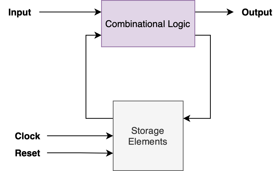
In order for sequential logic devices to work, we need to obey the dynamic discipline and the t1 and t2 constraints. Failure to obey that might put the device into the metastable state.
Here are the key points from this notes:
- General structure of sequential logic devices:
- Dynamic discipline: The hold time constraint (t1) and setup time constraint (t2) ensure the proper operation of sequential circuits by guaranteeing that data is reliably transferred between flip-flops in a sequential circuit. They prevent timing violations that could lead to incorrect operation of the circuit (incorrect propagation of signals). t1 ensures data from the upstream register remains stable long enough after the clock edge to satisfy the hold time of the downstream register. t2 ensures valid data arrives at the downstream register before the next clock edge with sufficient setup time.
- \(t_{cd}\) and \(t_{pd}\) computation of sequential logic devices: \(t_{cd}\) and \(t_{pd}\) are computed based only on the downstream combinational logic relative to the clock input, not user inputs.
- Metastable state: Occurs in flip-flops when the input changes too close to the clock edge, violating setup or hold time. In this state, the output is neither a stable 0 nor 1 and may oscillate or settle unpredictably. It arises because flip-flops internal feedback cannot resolve conflicting signal states quickly. We can mitigate metastability (but cannot completely avoid it) by using synchronizers and ensuring that dynamic discipline is obeyed.
Appendix
\(T_{setup}\) and \(T_{hold}\)
If you’re interested to know why the dynamic discipline has those specific constraints (\(T_{setup}\) and \(T_{hold}\)), read this section. If this is too much for you, you can skip it. You won’t exactly lose in exam if you skip it, just that your knowledge wont be whole.
How long is \(T_{setup}\) and \(T_{hold}\) approximately?
\(T_{setup}\) is approximately measured as \(2 \times t_{pd}\) of the components that make up the D-latch. \(T_{hold}\) is approximately measured as \(t_{pd}\) of the components that make up the D-latch. This \(t_{pd}\) is not the same as the \(t_{pd}\) of the entire sequential logic circuit (see section below)
As explained in the previous notes, \(t_{pd}\) is the propagation delay of the combinational logic devices (components) that make up a D-latch, e.g: a multiplexer, which has a \(t_{pd}\) value. The multiplexer can be made using a handful NAND gates. To clarify, this \(t_{pd}\) is the propagation delay of that multiplexer or components (combinational logic devices) that are used to make up a D-latch.
Think!
Why are the lengths for \(T_{setup}\) and \(T_{hold}\) dependent on the the \(t_{pd}\) of the components that make up the D-latch?
For \(T_{setup}\), you can figure this out by estimating how long you should wait to ensure that the output signal at Q reflects what was supplied at D (requires \(1\times t_{pd}\)), and to ensure that this output at Q maintains this value when CLK at G turns 0 (from Q’, requires another \(1\times t_{pd}\)).
For \(T_{hold}\), you can figure this out by realising that CLK is an input to the D-latch system as well, and the device needs some time (\(1\times t_{pd}\)) to realise that it is in memory mode after CLK turns to a valid 0. Throughout this brief period. of time, the input at D must be held valid/stable.
The Lenient Mux
Notice that Q is also an input to the MUX. We will meet a problem if 1-to-0 transition on G causes the Q output to become invalid at a brief interval (even when D is held stable obeying \(T_{setup}\) and \(T_{hold}\)).
Thus, we assume that the MUX used in a latch is a lenient MUX. A lenient MUX is a MUX where a 1-to-0 transition on G doesn’t affect the validity of Q output if certain prerequisite holds.
In particular, a lenient MUX WILL produce a stable and valid Q as long as either of 3 conditions below is fulfilled:
- When G is 1 (we are loading the latch), once D is valid for as long as half of \(T_{setup}\) (1 \(t_{pd}\)), we guarantee that Q will be stable and valid (reflecting D) independently of Q’ initial value. This allows Q to be unaffected by Q’ as it is overwriting Q’ when new values from D has just arrived.
- When D is valid for as long as \(T_{setup}\), we guarantee that Q will be stable and valid (reflecting D) independently of G. This ensures that a 1-to-0 transition on G doesn’t contaminate Q output
- When G is 0 (memory mode) and Q has been stable for at least \(T_{hold}\), then Q will no longer be affected by subsequent transitions on D input. Note that the only way for Q to be stable for this long when G has just turned to valid 0 is fulfilled by D, it should be held stable for at least \(T_{hold}\) for this effect to happen.
The truth table for the lenient MUX is as follows:
| G | D | Q’ | Q |
|---|---|---|---|
| 1 | 0 | X | 0 |
| 1 | 1 | X | 1 |
| 0 | X | 0 | 0 |
| 0 | X | 1 | 1 |
| X | 0 | 0 | 0 |
| X | 1 | 1 | 1 |
| X | 0 | 1 | X |
| X | 1 | 0 | X |
DFF Timing Constraint
To obey the dynamic discipline, there exist this timing constraint for the D Flip-Flop configuration:
\[t_{CD_{master}} \geq t_{H_{slave}}\]Imagine the exact moment when the INV CLK seen by master (latch) changes from 0 to 1, at the same time, the CLK signal seen by slave (latch) changes from 1 to 0. This transition by the CLK is not immediate and there is a short time window where the CLK goes from (valid) 1 to invalid value to (valid) 0.
This implies that the master goes into write mode while the slave goes into memory mode simultaneously.
However, the \(\star\) at the output of the master cannot change immediately in order to fulfil the \({t_{H}}\) requirement of the slave.
The \(\star\) has to retain its previous valid value (when the clock was valid) and cannot immediately do the following before the \({t_{H}}\) requirement of the slave is fulfilled:
- Become invalid due to transition in the CLK value, or
- Reflect whatever new input is given at D port of the master latch, even though the master latch is at the
writemode.
This means the contamination delay of the master latch (time taken on signal on \(\star\) is be invalid after CLK at G port becomes invalid) has to be at least as large as the hold time of the slave latch so that the Flip-Flop system obeys the dynamic discipline.
t1 and t2 Constraint Derivation
t1 constraint
The \(t_1\) constraint ensures that the \(t_H\) requirement of the downstream register, R2, is fulfilled by the devices thats put upstream (before it), that is CL and R1 in the example above.
- When the CLK rises at \(t_i\), both R1 and R2 are “capturing” different values, simultaneously.
- R1 is receiving current input value at \(t_i\), while R2 is receiving the computed old input value that was produced by R1 at \(t_{i-1}\).
- The devices upstream of R2 has to help to hold on to this old \(t_{i-1}\) values for the \(t_H\) of R2 to be fulfilled before responding to the rising edge of the clock and producing new values.
t2 constraint
The \(t_2\) constraint ensures that the clock period is long enough for three things to complete:
- Valid signal to be produced at the output of R1 and
- Signal to propagate through CL in between, and
- Signal to be set-up at the downstream register R2 (for
memorymode).
Once again, BOTH \(t_1\) and \(t_2\) constraints must be fulfilled within any paths between two connecting DFFs in a circuit, in order for the overall circuit to obey the dynamic discipline.
\(t_{pd}\) of CL
We can call the \(t_{PD} CL\) (propagation delay of the CL) as the time taken to do actual work or logic computation.
It should be clear by now why the input to this CL must be stable for at least \(t_{pd}\) for it to have meaningful output, and how our new circuit with DFFs (obeying dynamic discipline, \(t_1\), and \(t_2\) constraint) guarantees this – something that unreliable external input alone cannot guarantee if it were to be fed directly to the CL units.
The propagation or contamination delays of a Flip-Flop is not considered a logic computation, because unlike combinational logic devices (that can be made to implement functionalities such as addition, subtraction, boolean expressions, etc), a Flip-Flop does not implement any other special functionalities except to function as a memory device.
Non-Ideal Clock and \(t_{slope}\)
The \(t_1\) and \(t_2\) formulas assume the clock transitions instantaneously between valid 0 and valid 1. Under this idealization there is a single well-defined clock edge, and all reference points for \(t_{CD}\), \(t_{PD}\), \(t_H\), and \(t_S\) coincide at that edge. In reality every clock has a finite transition time \(t_{slope}\) during which the voltage is neither valid 0 nor valid 1. This is the same window that sits between \(T_{setup}\) and \(T_{hold}\) as noted earlier.
Consider the timing diagram below using a simple setup with one upstream DFF R1 and one downstream DFF R2 with differing timing specs:
Effect on \(t_1\) (Hold Constraint)
The two quantities in \(t_1\) have mismatched starting reference points:
- \(t_{CD}\) of R1 is measured from when CLK begins rising (leaves valid
0), indicated by timestampBtoDabove. - \(t_H\) of R is measured from when CLK finishes rising (reaches valid
1), , indicated by timestampCtoDabove.
These are separated by exactly some amount of time \(t_{slope}\) (timestamp B to C) which is the transition time of the rising CLK signal. The physically precise constraint is:
However, \(t_{CD}\) and \(t_H\) values reported on datasheets are both measured from the same defined reference point on the clock edge, for instance the 50% VDD threshold crossing somewhere between timestamp B anc C. Because both quantities share the same measurement start time, there is no reference-point mismatch between them in the first place. The standard formula \(t_{CD_{R1}} + t_{CD_{CL}} \geq t_{H_{R2}}\) therefore holds directly with datasheet values, and no explicit \(t_{slope}\) correction term is needed.
Effect on \(t_2\) (Setup Constraint)
The two quantities in \(t_2\) also have mismatched ending reference points:
- \(t_{CLK}\) is measured from when CLK has just reached valid
1to the next valid1(timestampCtoH). This technically includes two \(t_{slope}\). - \(t_H\) of R is measured from when CLK finishes rising (reaches valid
1), indicated by timestampCtoDabove.
This means that \(t_{CLK}\) and \(t_H\) does not have the same ending reference point. The slope at the end of the period therefore eats into the available propagation budget. The physically precise constraint is therefore:
\[t_{PD_{R1}} + t_{PD_{CL}} + t_{S_{R2}} \leq t_{CLK} - t_{slope}\]Similarly in practice this doesn’t matter anyway. \(t_{S}\) and \(t_{CLK}\) values reported on datasheets are both measured to/from the same defined reference point on the clock edge, for instance the 50% VDD threshold crossing of CLK signal. With this same ref point, there is no mismatch between the tsetup deadline and the end of the clock period. The standard formula \(t_{PD_{R1}} + t_{PD_{CL}} + t_{S_{R2}} \leq t_{CLK}\) therefore holds directly with datasheet values, and no explicit \(t_{slope}\) correction term is needed.
Just for curious readers
This whole \(t_{slope}\) discussion is just to show why the idealization is safe, but the practical takeaway is simply that the clock transition is treated as instantaneous. There is therefore no \(t_{slope}\) term in either \(t_1\) or \(t_2\), and the standard formulas hold directly. Everything else in the appendix is just the deeper justification for the curious reader.
About CPU Clock
This is a supplementary knowledge, for those who are curious only.
Throughout this lecture, we have learned how clocks make it easier to synchronize various combinational logic devices.
If you have difficulties remembering why synchronisation is required, remember assembly line. Ever seen an assembly line? People and machines working in sync to get the job done in the fastest and most efficient manner? Remember the sync part, that is the key. How are they so synchronized?
/https://tf-cmsv2-smithsonianmag-media.s3.amazonaws.com/filer/1c/11/1c113495-5153-4040-b7ea-5a37acf4d525/ford_assembly_line_-_1913.jpg)
Our CPU is very similar to that. It’s a giant synchronous circuit consisted of billions of transistors working together to compute results together. A CPU is typically reported with a clk rate (something around 3-4 Ghz in 2023); that’s our clock signal: a timing signal, like a conductor in an orchestra or the constant humming of machines in a factory that keeps up the assembly line’s tempo.
Our combinational logic devices will still work (to an extent) without adding clocks, but its functionality will be primitive. It will not be able to process series of inputs and outputs in an orderly (pipelined) fashion, and it will not be able to compute an output based on sequences of input (no memory device).
But where do clocks come from? How are they made and how can they produce such a high frequency for our CPUs to run?
The clock signal is commonly (but not always, there are other techniques too) produced mechanically using quartz crystals oscillators. When we apply a voltage source to a small thin piece of quartz crystal, it begins to change its shape and vibrate (a characteristic known as the piezo-electric effect). This characteristics produces a mechanical force. The frequency of which the crystal is going to oscillate varies, depending on the oscillator’s topology. We typically call this the base frequency of our clock. We then can build other circuits to multiply (boost) or divide (slow down) this frequency to run different components in our PC at different speed depending on the specifications.
For example in a multicore CPU, each core might have an independent multiplier circuit. Cores that are underutilised can run slower while cores under heavy load can run faster (e.g: Intel Turbo Boost). Your RAM also need a different clock speed than your CPUs.