 50.002 CS
- Sharing a Single RAM Between CPU and GPU
50.002 Computation Structures
Information Systems Technology and Design
Singapore University of Technology and Design
Sharing a Single RAM Between CPU and GPU
Module Code
Refer to this repository for the source code (verilog).
The relevant files for this design are:
shared_ram_gpu_cpu.v: Top-level time-multiplexer and GPU cache registersimple_dual_port_ram.v: Underlying BRAM primitive (posedge-clocked, single read port, single write port)register.v: Generic synchronous register used as the GPU output cachetb_shared_ram.v: Testbench covering writes, reads, concurrent access, and latency checks
Overview
A renderer (GPU-ish, e.g: VGA driver) and a CPU both need to read from the same screen buffer RAM. The problem is that a typical BRAM has only two ports: one read port and one write port, for simultaneous reads and writes at different addresses. The write port is straightforwardly owned by the CPU; it only writes. The read port, however, must be shared: the GPU reads every single pixel clock to fetch the current cell’s character and color, and the CPU also needs to read back values it has written.
The solution here is time-division multiplexing of the single read port, orchestrated entirely by the relationship between two clocks: a 50 MHz clock (clk50) and a 25 MHz clock (clk25). No arbitration logic, no handshake, and no FSM needed. The two clock edges carve the time axis into alternating CPU and GPU slots, and the mux select is literally just clk25.
This notes is written with the assumption that the GPU runs on 25Mhz clock e.g: for VGA. You can adjust the logic accordingly for different clock rates.
Assumptions
Here’s the hardware assumptions for this setup:
- Memory (BRAM) contains data only, not instruction
- Instruction memory is separate from data memory (Harvard Style)
- Modules needs to read and write simultaneously to the data memory in a single cycle to different address
- PC regfile has combinational read ports and synchronous write port
Dual-Read Port BRAM Configuration
For a single BRAM primitive (RAMB36E1 on Artix-7), we have:
- 2 ports total, A and B
- Each port can be read/write independently
- So maximum is 2 read ports and 2 write ports, but they share the same 2 physical ports
The configuration explained above: read and write to different addresses independently is the standard usage. This is what you get if you use simple_dual_port_ram in Alchitry Labs
However, you can also create a dual-port BRAM with the following specs instead if you don’t need to read/write simultaneously at the different addresses:
- Port A: Read/Write to address X
- Port B: Read from address Y
Therefore you can utilise the two ports available on the BRAM for independent reads, and one of the ports has shared read/write.
module dual_port_bram #(
    parameter ADDR_WIDTH = 14,
    parameter DATA_WIDTH = 8
)(
    // Port A: CPU read/write
    input                       clk_a,
    input  [ADDR_WIDTH-1:0]     addr_a,
    input  [DATA_WIDTH-1:0]     wdata_a,
    input                       we_a,
    output reg [DATA_WIDTH-1:0] rdata_a,

    // Port B: GPU read only
    input                       clk_b,
    input  [ADDR_WIDTH-1:0]     addr_b,
    output reg [DATA_WIDTH-1:0] rdata_b
);
    (* ram_style = "block" *)
    reg [DATA_WIDTH-1:0] mem [0:(1<<ADDR_WIDTH)-1];

    // Port A: CPU
    always @(posedge clk_a) begin
        if (we_a)
            mem[addr_a] <= wdata_a;
        rdata_a <= mem[addr_a];
    end

    // Port B: VGA
    always @(posedge clk_b) begin
        rdata_b <= mem[addr_b];
    end

endmodule
If your system is okay with the above design, then you can skip this guide entirely and let CPU and VGA read from the BRAM independently without multiplexing.
Note that rdata_a on Port A gives you the old value at addr_a even on a write cycle (read-first mode). If you want the new written value to appear on rdata_a immediately, change Port A to:
always @(posedge clk_a) begin
    if (we_a) begin
        mem[addr_a] <= wdata_a;
        rdata_a     <= wdata_a;  // write-first mode
    end else begin
        rdata_a <= mem[addr_a];
    end
end
Which mode you want depends on whether your CPU ever reads and writes the same address in the same cycle.
Assumption
This guide is written with the assumption that you need simultaneous read/write at different addresses. Therefore, the modules that need to read from the BRAM have to share the read time slices. If you do not need this constraint, skip this guide entirely.
Clock Relationship
Two clocks are used. Their frequencies and phase are not arbitrary: they are carefully chosen so that their edges interleave in a predictable, non-overlapping pattern.
| Clock | Period | Posedge times | Negedge times |
|---|---|---|---|
clk50 |
20 ns | 10, 30, 50, 70 … | 20, 40, 60, 80 … |
clk25 |
40 ns | 20, 60, 100, 140 … | 40, 80, 120, 160 … |
The critical invariant is: Every rising edge (posedge) of clk25 is aligned with a falling edge (negedge) of clk50.
This means every clk25 half-period contains exactly one clk50 posedge in its interior, 10 ns after the clk25 edge. That 10 ns gap is the setup window available for the RAM to respond before any result needs to be captured.

Terminology
To facilitate the explanation better, we shall use these terms:
t: this is the time of eachclk25rising edget+10: 10 ns after the rising edge ofclk25, which is the first rising edge ofclk50aftertt+20: 20 ns after the rising edge ofclk25, which is equivalent to falling edge ofclk25t+30: 30 ns after the rising edge ofclk25, which is the second rising edge ofclk50aftertt+40: 40 ns (one full perio ofclk25) after the rising edge ofclk25
Similarly, t+10 is equivalent to t+50, etc.
Time-Sliced Read Port Mux
The read address to the RAM is selected combinationally based on clk25:
assign ram_raddr = (clk25 == 1'b1) ? cpu_addr : gpu_addr;
- From
ttot+20, whenclk25 = 1(high half, 20 ns wide): the RAM reads the CPU address - From
t+20tot+40, whenclk25 = 0(low half, 20 ns wide): the RAM reads the GPU address
Because the BRAM is posedge-clocked on clk50, the address that gets latched and read is whichever address was stable when the clk50 posedge arrived.
- Data BRAM captures read address request from CPU at
t+10 - Data BRAM captures read address request from GPU at
t+30
Since every clk25 edge leads a clk50 posedge by 10 ns, the new address is always stable well before the RAM samples it.
Clock Specifications
clk50
This is the 50 MHz master clock with a period of 20ns.
This is the fastest clock in the system and is the reference everything else is derived from or phased against. All sequential elements that need to capture data from the RAM use this clock or its inverse. Posedges land at t = 10, 30, 50, 70, … and negedges land at t = 20, 40, 60, 80, …
clk25
This is the 25 MHz pixel clock with a period of 40 ns.
This is the GPU clock. We use 25MHz as an example here because it’s common to drive VGA with it. The GPU issues one read address per pixel clock, and the CPU is given access to the shared RAM in the complementary half-period. clk25 is not just any 25 MHz clock. It’s phase relative to clk50 is the entire basis of the design’s correctness.
The defining constraint is: every rising edge of clk25 is aligned to a falling edge of clk50.
Because clk25 is exactly half the frequency of clk50, this alignment automatically guarantees that every falling edge of clk25 is also aligned to a falling edge of clk50. In other words, both transitions of clk25 land on clk50 negedges, and the clk50 posedges always fall in the interior of a clk25 half-period, never at the boundary. Look at this waveform again to internalise that.
Each clk25 half-period is exactly 20 ns wide.
- Within that 20 ns window, one
clk50posedge falls at the 10 ns midpoint (red box) - This midpoint posedge is when the RAM does its work.
- The 10 ns before it is the address setup window (yellow box), and the 10 ns after it (ending at the next
clk25edge) is the RAM output propagation window before any capture happens (green box).

Generating Clock using MMCM
You should use Vivado clock_wiz or equivalent to generate the clock signal properly and not use other signals as clock. Read this handout for more information.
- Give appropriate
phasevalue in the Clocking Wizard window to align the 25Mhz and 50Mhz clock properly - You will need these clock signals:
clk100: 100Mhz (just in case you need the original clk for other components unrelated to this)clk50: 50Mhz (for data & instruction BRAM)clk25: 25Mhz (for CPU PC reg, and GPU/driver reg)clk25_n: 25Mhz (phase: 180, for CPU regfiles)
- Once generated, use it to drive the
clkport of the RAM, CPU, GPU, etc
Data RAM clock: clk50
The underlying BRAM is clocked on posedge clk50. This is the moment the RAM latches the current ram_raddr and produces ram_rdata on its output. Because the BRAM is synchronous, ram_rdata is not valid immediately after the address is driven but it only updates after a clk50 posedge has occurred with the address stable at its input.
The RAM sees one clk50 posedge per clk25 half-period: at one during the CPU slot (t+10) and one during the GPU slot (`t+30), and each time it captures whatever address the mux is currently presenting.
Warning: Detecting Clock Edges
If your CPU or GPU logic runs on clk100 and you need to detect edges of clk25 to generate single-cycle enables, you cannot sample clk25 directly with clk100. See this handout for why, and for the correct counter-based approach.
CPU Slot Timing
The CPU drives its address at posedge clk25 (which is a clk50 negedge), this is denoted as the white box in the diagram below. Consecutively, GPU timing is represented in purple box. At this moment clk25 goes high and the mux selects cpu_addr.
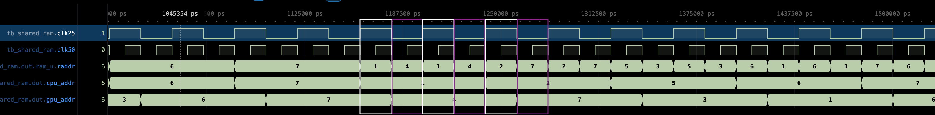
posedge clk25 = t=20   CPU drives cpu_addr, mux selects cpu_addr
posedge clk50 = t=30   RAM latches raddr = cpu_addr, ram_rdata becomes valid after delta
negedge clk25 = t=40   cpu_rdata_raw wire valid, CPU can safely read it
cpu_rdata_raw is a wire directly from ram_rdata, with no register in the path. This means it becomes valid roughly 10 ns after the clk50 posedge, and is fully settled well before negedge clk25 at t=40.
assign cpu_rdata_raw = ram_rdata;
CPU read latency from address driven to data readable (at the RAM’s read data port) is half a period of 50 MHz clock (10 ns).
CPU PC and REGFILE clk
PC on posedge of
clk25, REGFILE on negedge ofclk25The PC should be clocked to rising 25MHz edge. Every posedge 25MHz the PC advances to the next instruction, issues the new address to instruction RAM, and the CPU begins execution. The full high half of the 25MHz period is the execution window. At the falling edge, the regfile commits and the CPU is idle for the rest of the cycle.
RAM Cache for CPU
There is no need to cache the RAM result to the CPU, as the CPU can be made to stall during negedge clk25. It should have completed instruction execution within posedge clk25.
Stalling the CPU
You can stall the CPU in the low level of clk25 by making its regfile clocked on clk25_n directly, and the pc reg clocked on clk25.
Assumption
We assume that instruction BRAM is exclusive to the CPU and only data BRAM is shared between CPU and GPU. Read assumptions section above.
This clock setup gives 10ns of setup (from t+10 to t+20) and 10ns of hold (from t+20 to t+30) margin during data LD, so the regfile captures the correct RAM data cleanly with no modifications to the CPU.
GPU Slot Timing
The GPU drives its address at negedge clk25 (which is also a clk50 negedge). At this moment clk25 goes low and the mux switches to gpu_addr.
negedge clk25 (t+20) = GPU drives gpu_addr, mux selects gpu_addr
posedge clk50 (t+30) = RAM latches raddr = gpu_addr, ram_rdata becomes valid after delta
posedge clk25 (t+40) = GPU cache register captures ram_rdata, CPU slot starts
The GPU MUST produce a new read address request @negedge clk25. If your driver’s address is latched, ensure you are computing the address early (lookahead) so there’s no terrible pixel offset. If you are combinationally processing the GPU address output, make sure it doesn’t take longer than 10 ns. This is the time between negedge clk25 and the next posedge clk25 (ram issues new read output).
Caching RAM’s output for GPU
Unlike the CPU path, the GPU result cannot be read as a raw wire at the right time because we need the RAM result for the entire period of clk25 for certain drivers like VGA to work.
By t+40, the system has already crossed into the next clk25 posedge, which begins the CPU slot. The RAM will produce CPU’s read request at t+50 (which is t+10 in the next cycle). More often than not, we need to hold the GPU’s read request result stable across the next CPU period until the next GPU address call (i.e a full clk25 period). Therefore, it must be registered. This register is called gpu_cache_u.
The GPU Cache Register
The GPU cache is a standard synchronous register with three connections worth examining closely: its clock, its enable, and its data input.
  // GPU-side cache register
  register #(
      .W(32),
      .RESET_VALUE(0)
  ) gpu_cache_u (
      .clk(clk25),
      .rst(rst),
      .en (1'b1),
      .d  (ram_rdata),
      .q  (gpu_rdata_cached)
  );
It is clocked with clk25, so it captures inputs at .d at each rising edge of clk25 (t+40). It is always enabled.
Cache clock
The cache’s job is to cache the gpu’s read request and it’s driven by clk25 posedge. At each clk25 posedge, the RAM’s output would’be been stable for at least 10ns (green box) and will remain so for another 10ns.

The cache’s output remains stable for the entire duration denoted by the pink box, which is a full 25MHz period (40ns), until new address is supplied by the GPU at the falling edge of the 25MHz clock (if any). In short, capturing on the posedge clk25 gives maximum setup margin on the RAM output.
Data RAM Write Port
The CPU writes directly through to the Data RAM with no time-slicing needed.
ST Timeline
The underlying simple_dual_port_ram module produced by Alchitry labs has separate read and write ports. CPU writes (ST instructions) go to the write port (clocked on clk50 posedge), and reads go to the shared read port described above. The write requests go as follows:
- At
t,PCissues new read (instruction) address that goes to instruction memory (unshared) - At
t+10, instruction data is produced by instruction memory (clocked atclk50) - If this instruction is a
ST, the regfile combinational read ports can produce the requested data to store fromt+10+euntilt+50(next instruction received) - The data RAM received Write signals at
t+30, and perform theSTthen
At t+30, the GPU issues another read request, but there’s no write-read conflict between CPU writes and GPU reads because they use separate physical port paths.
If the CPU writes and the GPU reads the same address in the same clk25 period (at t+30), the GPU will see the newly written value in its cache output one clk25 period later (after the read completes at the next clk50 posedge following the GPU address being placed on the mux). The testbench verifies this in Phase 3.
LD Must be 2 Cycles
Since there are two reads: instruction read and LD data read, and both reads are combinational, we need to ensure that LD data (Mem[EA]) is properly latched by the regfile at t+20. However this is impossible given our setup:
- At
t,PCissues new read (instruction) address that goes to instruction memory (unshared) - At
t+10, instruction data is produced by instruction memory (clocked atclk50). Suppose this is aLDinstruction - That means, the data RAM cannot issue the requested data at
t+10as instruction is only received att+10. We need some time to computeEAfor theLD - The registers that are latching at
t+20(negedgeclk25) is not capturing the right read request from the RAM. It is in fact, capturing whateverMem[EA_STALE]whereEA_STALEis whatever read request CPU gives att+10. - This instruction is maintained all the way until
t+50, when new instruction arrived. - At this time, the data RAM received the
EAgiven byLDinstruction int+10, and producedMem[EA]att+50 - However the new instruction at
t+50might not beLDanymore, so we entirely will missMem[EA]produced by the Data RAM
To fix this, LD instruction must be 2 CPU cycles. If you are making the assembler, simply printout the LD instruction twice. You can find more details about it here.
Latency
The diagram below shows a timing plot of a full GPU slot followed by a CPU slot.
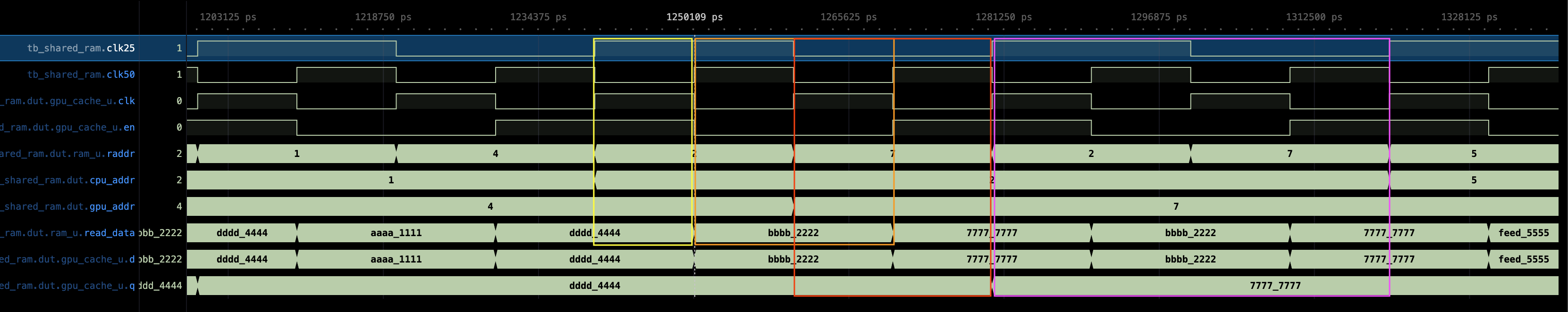
Legend:
- Yellow box: CPU latency (10ns)
- Orange box: CPU read request outputted (at RAM’s read data output), stable for 20ns.
- Red box: GPU latency (with reference to GPU cache), 20ns
- Pink box: GPU read request outputted at the
.qport of GPU cache, stable for 40ns.
Integration Notes
Using Other Clock
In this test bench, CPU issues address exactly at posedge clk25, and GPU issues address exactly at negedge clk25. It is important that you ensure this in your design by not using any registers driven by other clock, e.g; 100Mhz.
If you have certain pipelined address request such as follows, where address is a dff driven by other clock, say clk100,
    dff address[N](.clk(clk_100))

    if (clk_25_fall){
        address.d = address.q + 1
    }

    gpu_address_read_request = address.q
Then there will be some latency (~10ns) after the falling edge of clk25 before GPU’s read address request is valid. This might violate the timing constraint, where we require GPU’s read address request to be valid before the RAM captures it at t+30 (end of green box).

An important consequence for the VGA use case: by the time the GPU cache produces a result at posedge clk25, the VGA renderer is already 50% through its clk25 period. The renderer’s pipeline must account for this one-half-period offset when deciding which address to issue relative to which pixel it expects to draw. We address it in this guide.
Port Reference
shared_ram_gpu_cpu
| Port | Direction | Width | Description |
|---|---|---|---|
clk50 |
input | 1 | 50 MHz clock, drives BRAM |
clk50_n |
input | 1 | 50 MHz clock, drives en_gpu register |
clk25 |
input | 1 | 25 MHz clock, acts as read-port mux select |
rst |
input | 1 | Synchronous reset for GPU cache register |
same_phase |
input | 1 | Reserved (tie to 0 for standard operation) |
cpu_addr |
input | 3 | CPU read/write address |
cpu_wdata |
input | 32 | CPU write data |
cpu_we |
input | 1 | CPU write enable |
gpu_addr |
input | 3 | GPU read address |
cpu_rdata_raw |
output | 32 | CPU read data (wire directly from RAM output) |
gpu_rdata_cached |
output | 32 | GPU read data (registered, stable for full CPU slot) |
ram_read_data_dbg |
output | 32 | Debug: current RAM read data (same as cpu_rdata_raw) |
ram_raddr_dbg |
output | 3 | Debug: current address on RAM read port |
ram_write_enable_dbg |
output | 1 | Debug: current RAM write enable |
Testbench Phases
The testbench (tb_shared_ram.v) validates the design through eight phases:
- Phase 1: CPU preloads addresses 1 through 4 with known values. GPU is parked on address 0 (uninitialized, expect X).
- Phase 2: GPU reads back the four values written by the CPU. Checks that each read returns the correct value and measures cache latency.
- Phase 3: CPU writes and GPU reads the same address in the same
clk25period. Confirms the GPU sees the freshly written value exactly oneclk25period later. - Phase 4: CPU writes one address while the GPU reads a different address. Confirms there is no cross-address corruption.
- Phase 5: CPU reads raw and GPU reads cached on the same addresses. Both results checked for correctness and latency.
- Phase 6: Rapid interleaved reads across all written addresses, alternating CPU and GPU addresses every slot. Every check reports measured latency; all should show 20 ns consistently.
- Phase 7: GPU holds the same address for four consecutive slots. Confirms the cache holds its value stably between GPU slot updates while the CPU slot runs in between.
- Phase 8: CPU overwrites an address while the GPU is repeatedly reading it. Confirms the GPU cache reflects the new value in the very next slot after the write completes.