 50.002 CS
50.002 Computation Structures
Information Systems Technology and Design
Singapore University of Technology and Design
Driving SN74HC595 with an FPGA
Driver Code
You can download the driver code from here.
The entire repository with demo code can be found here.
How SN74HC595 Works
The SN74HC595 is an 8-bit serial-in, parallel-out shift register with a second 8-bit storage (output) register behind it. You shift bits in serially, then latch them so the outputs update all at once.
It has separate clocks for shifting vs latching, and the outputs can be 3-stated (disconnected) using OE.
You can read this tutorial to understand more on how to connect the pins. It has many pinouts, so you still need to do lots of hardware work but the connection to the FPGA is minimal. This is particularly good if you have tons of LEDs to connect, and don’t mind raw soldering work but run out of pins from the FPGA.
Image taken from this video.
Pins
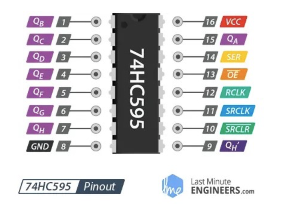
Here are the pin names and the corresponding label in the code:
SER(labeledds): serial data input.SRCLK(labeledshcp): shift clock; on each rising edge, the bit onSERenters the first stage and everything shifts along.RCLK(labeledstcp): latch clock; on a rising edge, the current shift-register contents copy into the storage register (this is what updatesQA..QH).OE(labeledoe): output enable;OE=1disables outputs (high-Z),OE=0enables outputs.SRCLR(labeledmr, active-low): direct clear of the shift register when low (independent of clocks).QH': serial output used for daisy-chaining to the next chip’sSER.QB-QH: parallel output to each LED. You need a resistor for each connection.
The basic “send pattern” sequence
Here are the general steps on how to pump the data in:
- (Optional) Disable outputs during shifting: set
OE=1(outputs high-Z). - For each bit (total
CHAIN * 8bits):- Put next bit on
SER(ds) - Pulse
SRCLK(shcp) low→high to shift it in
- Put next bit on
- Pulse
RCLK(stcp) low→high once to latch all 8 (or 16, 24, …) bits toQA..QH. - Enable outputs: set
OE=0to drive the pins.
Daisy-chaining
- With
CHAIN = N, you’re effectively building a 8N-bit shift chain: bits you clock in first will “move down the line” and eventually end up in the farthest chip after enoughSRCLKpulses. QH'is exactly there so the first chip can feed the second chip, and so on.
How the driver FSM maps to the datasheet behavior
IDLE: wait fornew, capturedatainto an internal register.LOAD: align so you don’t miss the first bit relative to your generated shift clock.TRANSFER: driveds, pulseshcpforCHAIN*8rising edges (shift operation).LATCH: pulsestcponce (copy shift to storage, updating outputs).RESET: pullmrlow briefly to clear the shift register.
Debug Notes
Clearing (SRCLR / mr) clears the shift register, not the outputs immediately. Outputs change only when you latch with RCLK.
If you ever tie SRCLK and RCLK together, the datasheet notes the shift register ends up one clock ahead of the storage register, which is why most designs keep them separate.