 50.002 CS
- Classifying FSM (Basic)
- An Incomplete State Machine (Basic)
- Constructing an FSM (Basic)
- Hardware Implementation of a state machine (Intermediate)
- State-Machine Timing Computation (Intermediate)
- FSM Possibility (Basic)
50.002 Computation Structures
Information Systems Technology and Design
Singapore University of Technology and Design
State Machine
Each topic’s questions are grouped into three categories: basic, intermediate, and challenging. You are recommended to do all basic problem set before advancing further.
Classifying FSM (Basic)
The diagram below illustrates the FSM diagram of a machine that has the same purpose. The circle that is bolded signifies the starting state.
State whether the following is true or false and explain your answer:
- Statement 1: “Diagram A illustrates a Mealy machine.”
- Statement 2: “Diagram B can be further minimized.”
What is the purpose of these FSMs?

Statement 1 is false because the machine in Diagram A has its output that depends only on its state. Statement 2 is **true**, we can minimise it into just two states because S1 and S2 are equivalent.
The purpose of both machines is to detect the presence of an edge and output a 1 once for the cycle where the edge happens, and 0 otherwise.
Your friend plot the timing diagram of the machine in Diagram A and obtain the following output:

Assume that the machine starts at S0. While referring to the FSM diagram up above, write the current state that occurs at instances [A], [B], [C], and [D] respectively.
We can obtain the answers easily by running the FSM step by step. At each labeled instance, the machine is at the following states:
[A]: S0,[B]: S2,[C]: S1,[D]: S0,
An Incomplete State Machine (Basic)
The ACME Company has recently received an order from a Mr. Wiley E. Coyote for their all-digital Perfectly Perplexing Padlock (P3):
- The P3 has two buttons (“0” and “1”) that when pressed cause the FSM controlling the lock to advance to a new state.
- In addition to advancing the FSM, each button press is encoded on the B signal (B=0 for button “0”, B=1 for button “1”).
- The padlock unlocks when the FSM sets the UNLOCK output signal to 1, which it does whenever the last N button presses correspond to the unique N-digit combination.
- The FSM should not fully reset if a valid prefix (1 bit) of the sequence is still present, so after an incorrect input, check if the last entered digit matches the beginning of the correct sequence.
Unfortunately the design notes for the P3 are incomplete. Using the specification above and clues gleaned from the partially completed diagrams below fill in the information that is missing from the state transition diagram with its accompanying truth table.
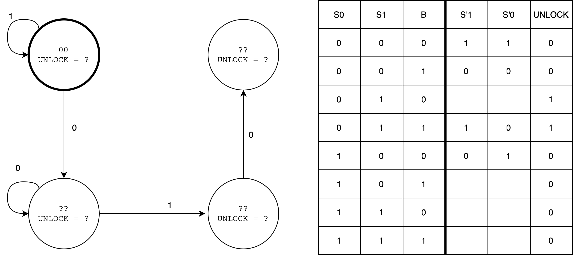
When done,
- Each state in the transition diagram should be assigned a 2-bit state name
S1 S0(note that in this design the state name is not derived from the combination that opens the lock), - The arcs leaving each state should be mutually exclusive and collectively exhaustive,
- The value for UNLOCK should be specified for each state, and the truth table should be completed.
Also, what is the combination of the lock?
This state machine is a Moore machine. The completed state transition diagram and truth table is as follows:
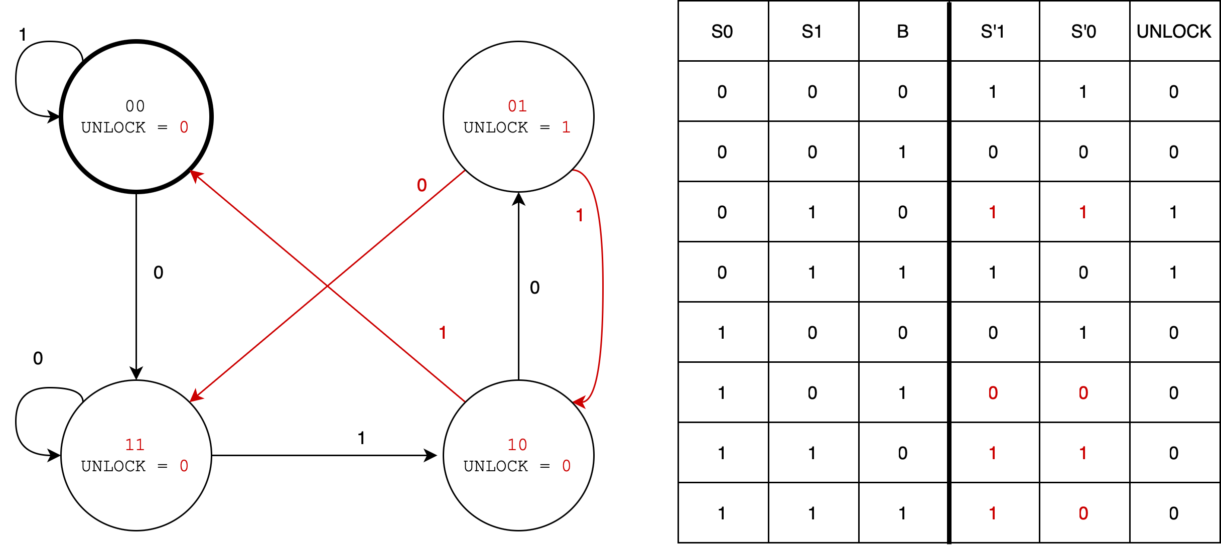
The combination for the lock is 010.
Constructing an FSM (Basic)
Construct a divisible-by-3 Moore FSM that accepts a binary number entered one bit at a time. The most significant bit entered first, and the FSM should indicate with an output light (1 bit) if the number entered so far is divisible by 3.
Hint
The FSM has 3 states.
Answer the following questions:
- Draw a state transition diagram for your FSM indicating the initial state and for which states the light should be turned on.
Show Answer
If the **value** of the number entered so far is `N`, then if digit `b` is entered next, the value of the new number `N'` is `2N + b`. Using this fact:
- If `N mod 3 == 0` then for some integer `p`,` N = 3p + 0`. After the digit b is entered, `N' = 6p + b`. So `N'` is `b mod 3`.
- If `N mod 3 == 1` then for some integer `p`, `N = 3p + 1`. After the digit b is entered, `N' = 6p + 2 + b`. So `N'` is `b+2 mod 3`.
- If `N mod 3 == 2` then for some integer `p`, `N = 3p + 2`. After the digit b is entered, `N' = 6p + 4 + b`. So `N'` is `b+1 mod 3`.
This leads to the following transition diagram where each state corresponds to each of the possible values of `N mod 3`.

- Construct a truth table for the FSM logic. Inputs include the state bits and the next bit of the number; outputs include the next state bits and the control for the light. Remember that this should be a Moore machine, so the output (light) should follow the current state output and not the next state.
Show Answer
$$ \begin{matrix} S_1 & S_0 & b & S_1' & S_0' & \text{light} \\ \hline 0 & 0 & 0 & 0 & 0 & 1 \\ 0 & 0 & 1 & 0 & 1 & 1 \\ 0 & 1 & 0 & 1 & 0 & 0 \\ 0 & 1 & 1 & 0 & 0 & 0 \\ 1 & 0 & 0 & 0 & 1 & 0 \\ 1 & 0 & 1 & 1 & 0 & 0 \\ \hline \end{matrix} $$
- Write down the boolean equation for the FSM.
Show Answer
The boolean equation for the FSM is: $$ \begin{aligned} \text{light } &= \overline{S_1} \cdot \overline{S_0}\\ S_1' &= \overline{S_1} \cdot S_0 \cdot \overline{b} + S_1 \cdot \overline{S_0} \cdot b \\ S_0' &= \overline{S_1} \cdot \overline{S_0} \cdot b + S_1 \cdot \overline{S_0} \cdot \overline{b}\\ \end{aligned} $$
Hardware Implementation of a state machine (Intermediate)
Consider the schematic of a machine as follows, which function is to: detect a sequence of three or more consecutive 1’s, and output: 1 after three or more consecutive 1’s, or 0 otherwise.

Let’s analyse the circuit by answering the questions below:
- If the circuit has an initial state of
AB=00, and the input att=0isx=0, what will the immediate next state be?Show AnswerThe immediate next state is:
AB = 00. You can easily trace this output from the circuit above. - If the circuit has an initial state of
AB=00, and the input att=0isx=1, what will the immediate next state be?Show AnswerThe immediate next state is:
AB = 01. You can easily trace this output from the circuit above. - If the circuit has a current state
AB=01, and the current input isx=1, what will the immediate next state be?Show AnswerThe immediate next state is:
AB = 10. You can easily trace this output from the circuit above. - If the circuit has a current state
AB=11, and the current input isx=1, what will the immediate next state be?Show AnswerThe immediate next state is:
AB = 11. You can easily trace this output from the circuit above. - If the circuit has a current state
AB=11, and the current input isx=0, what will the immediate next state be?Show AnswerThe immediate next state is:
AB = 00. You can easily trace this output from the circuit above. -
What are the state(s) that can go to state
AB=00as its next state?Show AnswerAll combinations:
AB=00, 01, 10, or11. You can prove it easily by brute force: checking ifAB = 00next if its previously set to some valueAB = ijgiven existing valuex. - What is the value of output
ywhen the current state isAB = 11and the current input isx = 0?Show AnswerTracing it out, we have
y=1. - The propagation delays for all the combinational logic gates and the flip-flops are
2ns. The clock frequency is100MHz. What is the worst case delay in nanosecond for the next states atAandBto appear (i.e. forAandBto be valid) after the inputxis changed to be a valid input. Assume that the initial statesABare given and fixed.Show AnswerFrom the frequency, we can compute the period of the clock to be
10ns.
For the worst case delay, we need to consider the scenario that inputxis propagated up to input of the register and it just missed theclkrise. It takes4nsto propagate through theANDandORgates, and another10nsto wait for anotherclkrise. Finally, it takes2nsto propagate through the register to produceAorB. Hence the worst case delay is4+10+2 = 16ns. -
The propagation delays for all the combinational logic gates and the flip-flops are
2ns. Eachdffhave th and ts of1nseach. If the clock frequency is not given, what is the maximum clock frequency (smallestclkperiod) that we can have for this device?Show AnswerThe clock period has to satisfy the feedback path (t2 timing constraint), that is made up with **tpd** of the
dff, **tpd** of theANDgate, **tpd** of theORgate, plus **ts** of the register. This adds up to2+2+2+1 = 7ns. Hence the maximum frequency is:$$\frac{1}{(7*10^{-9})}= 142.9MHz$$. - What are the output sequences from
t=0tot=15of the circuit when fed the following input (fed from left to right):1101 1111 1110 0010fromt=0tot=15respectively? Assume that the initial states areAB=00.Show AnswerGiven that the initial state is
AB=00, that makesB = 1att=0. This is doable the tedious way by simply tracing the outputysixteen times fromt=0tot=15. We can also deduce from the functionality of the device, that is to detect three consecutive1's and output0afterwards. The output sequence is therefore0000 0011 1111 0000fromt=0tot=15. repectively.
State-Machine Timing Computation (Intermediate)
Take a look at the following State Machine circuitry:

The device A2 has the following schematic:

It is made out of this device we call A000R with tcd = 1ns, and tpd = 3ns with the following schematic:

The truth table for A000R is as follows:
The timing specifications for other devices in the state machine is:
- The Mux has the following time specification: tcd =
1ns, and tpd =2ns. - The Registers has the following time specification: tcd =
2ns, tpd =5ns, ts =2ns, th =2ns.
Both A1 and A2 are combinational logic that contains A000R only. Unfortunately, the design for A1 is missing. We only know that A1 uses only A000R to compute the output and the next state function and that A1 has the same tpd as A2. The other information that we have is that the output of A1, X[2:0] is a sequence of decimal, [1, 2, 3, ... ] in the binary form, i.e. [001, 010, 011, ...].
Answer the following questions:
- How many bits should the constant
Z1have?Show AnswerSince one of the inputs to the MUXes are 3-bits, this hardware is implemented using three 2-input MUX.
Z1is essentially three bits, connected to each of the three copies of 2-input MUXes. - How many bits should the constant
Z2have?Show Answer1 bit. The number of bits of each input to a combinational logic device such as
A1does not depend on anything else or other inputs. - What is the decimal value of
Z1?Show AnswerSince
X[2:0]produces an increasing sequence from decimal value of1,2,3,4,...etc, we can easily guess that the the decimal value ofZ1should be0, such that when there's aRESET, the output of the registerR1is zero. - What is the decimal value of
Z2?Show AnswerZ2's decimal value is1. The same reason applies: since the sequenceX[2:0]produced byA1is increasing by 1, the input toA1should be 1 such that at *every* cycle, theres an addition of 1 to be produced atX. - What is the tpd of
A2in nanosecond?Show AnswerThe **tpd** of
A000Ris 3ns, hence the **tpd** ofA2is9nssince it is made out of threeA000Rmodules connected in series. - What is the minimum clock period in nanosecond?
Show Answer
The longest path that the clock period has to satisfy is
R1 -> A1 -> A2 -> Z1 -> R2. Hence we need to consider the **tpd** of all devices in its path (exceptR2) plus **ts** ofR2: 5+9+9+2+2 = 27ns. - What is the minimum tcd of
A1in nanosecond such that th of input (Z2) can be 0?Show Answer**tcd** of
A1has to be large enough so as to satisfy **th** ofR1. **th** ofR1is2ns, and **tcd** of the MUX is1ns. Therefore min **tcd** ofA1is2-1 = 1ns. - What is value of
A2’s tcd in nanosecond?Show AnswerThe **tcd** of
A2is basically the **tcd** of a singleA000R (1ns)since that is the shortest path from any input to any output inA2. - When
RESETis1for several cycles, what will be the value ofX[2:0]?Show AnswerWhen
RESETis1, the output ofR1will be000. Hence the value ofX[2:0]will be001.. - When
X’s output is sequences of value[1, 2, 3, ...], what is the value ofRESET?Show AnswerRESEThas to be0to enable the addition of the previous value of `X` to take effect, and form a new value of `X` in the next clock cycle.
Now, suppose that at time t=0, RESET signal is changed from 1 to 0, and X becomes 001. From then on, RESET remains 0:
- What is the decimal value of
O[2:0]at timet = 0?Show AnswerXis001andYis000att=0. Using the truth table ofA000Rand the schematic ofA1, we can deduce thatO[2:0]att=0is1. - What is the decimal value of
O[2:0]at timet = 1?Show AnswerXis010andYis001att=1. Using the truth table ofA000Rand the schematic ofA1, we can deduce thatO[2:0]att=1is3. - What is the decimal value of
O[2:0]at timet = 3?Show AnswerXis011andYis011att=2. Using the truth table ofA000Rand the schematic ofA2, we can deduce thatO[2:0]att=3is2.
FSM Possibility (Basic)
We saw that certain functions, such as parentheses checking, cannot be performed by any finite state machine. Which of the following can be performed by an FSM?
Assume, in each case, that the device is to take a series of 0s and 1s that represent the digits of a binary number entered left to right.
- The device is to have a single output, which is 1 only under this specific condition: when the last
277digits entered have been alternate1s and0s.Show AnswerYes. It is a bit tedious for `277` digits, but you should be able to sketch FSM for 3 or 4 digits.
-
The device is to have a single output, which is 1 only under this specific condition: when more 0s than 1s have been entered.
Show AnswerNo. Requires unbounded counting.
-
The device is to have a single output, which is 1 only under this specific condition: when the number entered thus far is divisible by 3.
Show AnswerYes, can be done by a 3-state machine.
-
The device is to have a single output, which is 1 only under this specific condition: when an odd number of 1s and and even number of 0s have been entered.
Show AnswerYes,, can be done with a 4-state machine.