 50.002 CS
- Introduction
- Memory Unit
- Part A: PC Unit
- Part B: REGFILE Unit
- Part C: CONTROL Unit
- Part D: Assemble Completed Beta
- The Motherboard
- Using BRAM for
firmware - Connecting it with hardware
- Compile and Run
- What next?
- Appendix
- Reset Conditioner
- Button Conditioner
- Edge Detector
50.002 Computation Structures
Information Systems Technology and Design
Singapore University of Technology and Design
(Verilog) Lab 6: Beta CPU
This is a Verilog parallel of the Lucid + Alchitry Labs Lab 6. It is not part of the syllabus, and it is written for interested students only. You still need to complete all necessary checkoffs in Lucid, as stated in the original lab handout.
If you are reading this document, we assume that you have already read Lab 4 Lucid version, as some generic details are not repeated. This lab has the same objectives and related class materials so we will not paste them again here. For submission criteria, refer to the original lab 6 handout.
Introduction
The goal of this lab is to build a fully functional 32-bit Beta Processor on our FPGA so that it could simulate simple programs written in Beta Assembly Language. It is a huge device, and to make it more bearable we shall modularise it into six major components:
- Memory Unit: the RAM or physical memory, separated into data and instruction memory.
- (Beta CPU Part A) PC Unit: containing the PC register and all necessary components to support the ISA
- (Beta CPU Part B) REGFILE Unit: containing 32 32-bit registers, WASEL, and RA2SEL MUX, plus circuitry to compute Z
- (Beta CPU Part C) CONTROL Unit: containing the ROM and necessary components to produce all Beta control signals given an
OPCODE - (Beta CPU Part D) ALU+WDSEL Unit: containing the ALU and WDSEL, ASEL, BSEL MUXes
- Motherboard: We assemble the entire Beta CPU using all subcomponents above and connect it to I/O
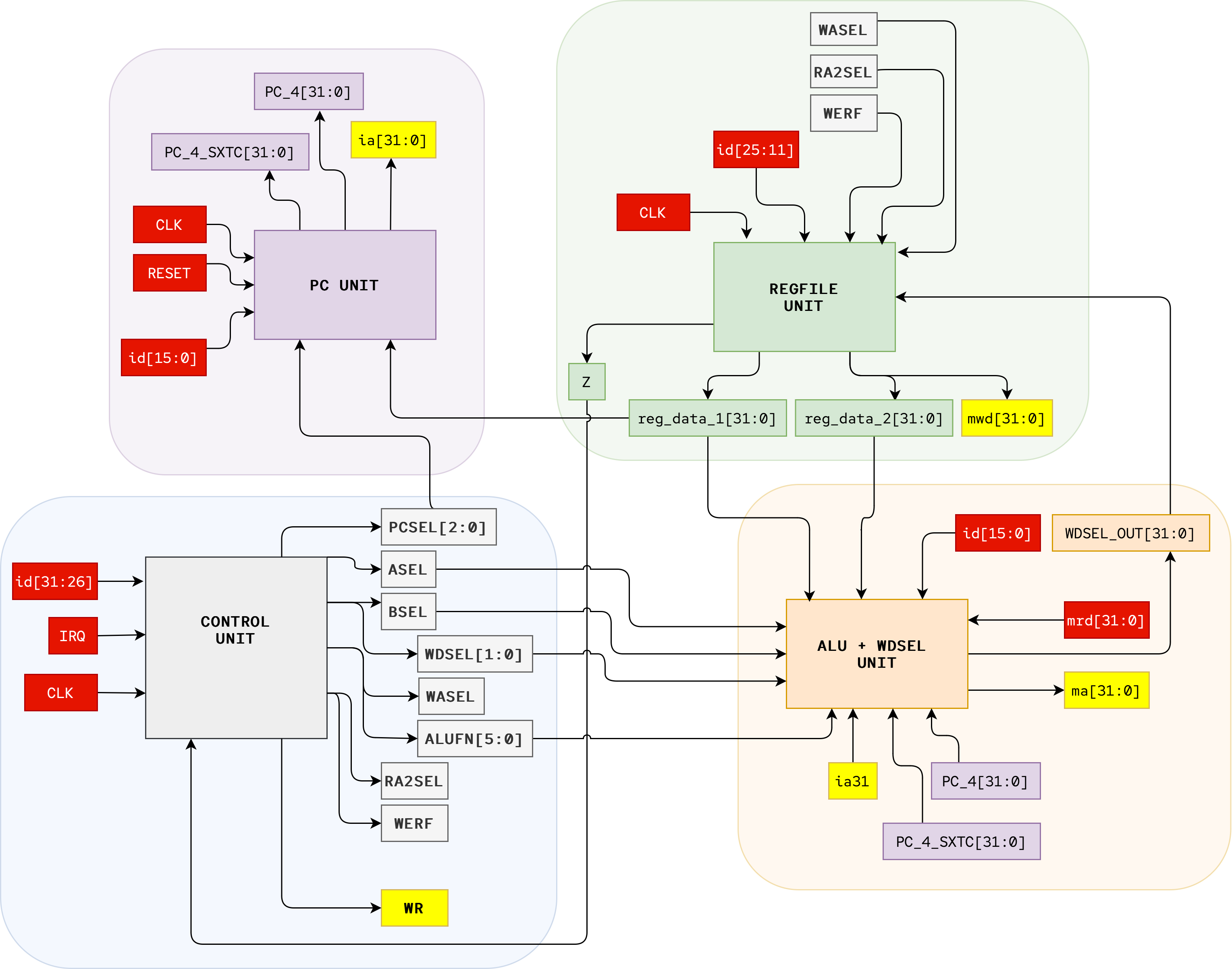
The signals indicated in red refers to external INPUT to our Beta, supplied by the Memory Unit. The signals illustrated yellow refers to our Beta’s OUTPUT to the Memory Unit.
Please study each section carefully as this will be beneficial not only for your 1D Project and Exam, but also to sharpen your knowledge in basics of computer architecture which might be useful in your future career as a computer science graduate.
Memory Unit
We strongly suggest that the memory Unit is made physically separated into two sections for ease of explanation and implementation:
- the instruction memory and
- the data memory
In practice, the data segment and the instruction segment are only logically segregated, so it would need to support two reads in a single cycle (for both data and instruction). They still share the same physical device we call RAM, but we implement them as two RAM blocks here to keep the Beta CPU wiring simple. For more details regarding 2R1W type of RAM and possible implementation in FPGA, see the appendix.
Below is a sample implementation of the memory unit that can be used to alongside your Beta CPU. It utilises a simple rom
(firmware) and simple_dual_port_ram (see sections below) provided by Alchitry Labs’ component library, which will utilise the BRAMs of the FPGA to implement the memory unit instead of using the limited LUTs.
// Byte-addressed inputs, word-aligned internally (addr >> 2)
module memory_unit #(
    parameter integer WORDS = 16
) (
    input wire clk,

    // data memory (byte addressing expected)
    input  wire [$clog2(WORDS)+2-1:0] raddr,
    input  wire [$clog2(WORDS)+2-1:0] waddr,
    input  wire [               31:0] wd,
    input  wire                       we,
    output wire [               31:0] mrd,    // 1-cycle latency

    // instruction memory (byte addressing expected)
    input wire [31:0] ia,
    output wire [31:0] id,  // combinational
    output wire [7:0] num_instr
);


  // instruction
  firmware_rom u_firmware_rom (
      .ia(ia),
      .id(id),
      .num_instr(num_instr)
  );


  localparam integer AW = $clog2(WORDS);

  // Convert byte address -> word address by dropping low 2 bits
  wire [AW-1:0] ra_word = raddr[AW+1:2];
  wire [AW-1:0] wa_word = waddr[AW+1:2];


  // Data memory: dual-port RAM (sync read on rclk, write on wclk)
  simple_dual_port_ram #(
      .WIDTH  (32),
      .ENTRIES(WORDS)
  ) data_memory (
      .wclk        (clk),
      .waddr       (wa_word),
      .write_data  (wd),
      .write_enable(we),

      .rclk     (clk),
      .raddr    (ra_word),
      .read_data(mrd)
  );

endmodule
Instruction Memory
The instruction memory can be implemented as a ROM since it’s supposed to be read-only. You can create submodule firmware and load different instructions in it based on the ia given.
Note that this module is implemented as combinational logic so it is not ideal if you have large number of instructions. If you have larger number of instructions then you need synchronous ROM (implemented as BRAM) and clock it with a signal that’s twice as fast as the beta cpu clock. We will address this in the later sections.
`timescale 1ns / 1ps

// ------------------------------------------------------------
// Firmware ROM (BYTE-addressed)
// memory_unit expects byte addresses, word-aligned internally.
// So we case on ia byte addresses: 0x000,0x004,0x008,0x00C,0x010...
// ------------------------------------------------------------
module firmware_rom (
    input wire [31:0] ia,  // byte address
    output reg [31:0] id,
    output wire [7:0] num_instr
);
  assign num_instr = 8'd5;
  always @(*) begin
    id = 32'h00000000;  // default (ILLOP / NOP depending on your ISA)

    // Strict word-aligned fetch by masking low 2 bits
    // This makes ia=0x...1/2/3 behave like ia=0x...0 (typical).
    // ignore the PC31
    case ({
      ia[30:2], 2'b00
    })
      31'h00000000: id = 32'hC03F0003;  // 0x000 ADDC(R31, 3, R1) --- main
      31'h00000004: id = 32'h90410800;  // 0x004 CMPEQ(R1, R1, R2)
      31'h00000008: id = 32'h643F0020;  // 0x008 ST(R1, 32, R31)
      31'h0000000C: id = 32'h607F0020;  // 0x00C LD(R31, 32, R3)
      31'h00000010: id = 32'h7BE3FFFB;  // 0x010 BNE(R3, main, R31)
      default:      id = 32'h00000000;
    endcase
  end
endmodule
For the case inside the firmware, we ignore ia31 (PC31), which is the Beta CPU’s status bit.
Data Memory
The Beta CPU can read or write the Data Memory. For ease of demonstration, data memory is implemented as a dual port RAM (read and write can be done independently in the same clk cycle), see appendix. That is why we have two address ports raddr and waddr.
read_dataoutputs the value of the entry pointed to byraddrin the previous clock cycle. If you want to read addressEA, setraddr = EAand wait one FPGA clock cycle forMem[EA]to show up.- We should avoid reading and writing to the same address simultaneously because the returned value is undefined (tool/FPGA dependent).
The interface is:
// for data memory (byte addressing expected)
input  raddr[$clog2(WORDS)+2],
input  waddr[$clog2(WORDS)+2],
input  wd[32],
input  we,
output mrd[32]
You should avoid reading and writing to the same address simultaneously. The value read in this case is undefined. Also, mrd outputs the value of the entry pointed to by raddr in the previous clock cycle. The unit is always reading based on whatever value is at raddr, so you can ignore mrd values if you don’t need it.
Memory Read
To load (read) data from memory, the Beta supplies the effective address EA on raddr. After one rising edge of clk, the memory outputs:
mrd[31:0] = Mem[EA]
Memory Write
To store (write) data to memory, the Beta supplies:
waddr= effective addressEAwd[31:0]= the 32-bit value to storewe= 1 to perform the write on the rising edge ofclk
The signal we must always be a valid logic value (0 or 1) at the rising edge of clk. If we = 1, the value on wd[31:0] is written into memory at the end of the current cycle. If we = 0, wd[31:0] is ignored.
Addressing Convention (Byte Address In, Word-Aligned)
We expect byte addresses to be supplied at ia, raddr, and waddr. However, our RAM blocks store 32-bit words, so the memory unit is word-aligned internally.
This means:
- We ignore the lower two bits of the address (
addr[1:0]). - Internally, the word index is
addr >> 2.
In Verilog, we implement this by slicing:
wire [AW-1:0] word_addr = addr[AW+1:2]; // drop addr[1:0]
As a result:
- Addresses
0x00,0x01,0x02,0x03all map to the same word (word 0) - Address
0x04maps to the next word (word 1) - Unaligned accesses are not supported (they are forced to the aligned word).
We could implement a strictly byte-addressable RAM by storing bytes (WIDTH=8) and using ENTRIES=WORDS*4, but then we must add additional logic to assemble 4 bytes into a 32-bit word (and handle byte enables on stores). For the Beta CPU memory unit here, we keep the design word-aligned for simplicity.
Testbench
You can use the following testbench to observe how the memory unit work:
`timescale 1ns / 1ps

module tb_memory_unit;

  // --------------------------------------------------------------------------
  // Params
  // --------------------------------------------------------------------------
  localparam integer WORDS = 16;
  localparam integer AWB = $clog2(WORDS) + 2;  // byte-address width for data mem ports

  // --------------------------------------------------------------------------
  // DUT I/O
  // --------------------------------------------------------------------------
  reg            clk;

  reg  [AWB-1:0] raddr;
  reg  [AWB-1:0] waddr;
  reg  [   31:0] wd;
  reg            we;
  wire [   31:0] mrd;

  reg  [   31:0] ia;  // instruction addr is now 32-bit
  wire [   31:0] id;
  wire [    7:0] num_instr;

  // --------------------------------------------------------------------------
  // Instantiate DUT
  // --------------------------------------------------------------------------
  memory_unit #(
      .WORDS(WORDS)
  ) dut (
      .clk(clk),

      .raddr(raddr),
      .waddr(waddr),
      .wd   (wd),
      .we   (we),
      .mrd  (mrd),

      .ia       (ia),
      .id       (id),
      .num_instr(num_instr)
  );

  // --------------------------------------------------------------------------
  // Clock
  // --------------------------------------------------------------------------
  initial clk = 1'b0;
  always #5 clk = ~clk;  // 100 MHz

  // --------------------------------------------------------------------------
  // Wave dump
  // --------------------------------------------------------------------------
  initial begin
    $dumpfile("tb_memory_unit.vcd");
    $dumpvars(0, tb_memory_unit);
  end

  // --------------------------------------------------------------------------
  // Helpers
  // --------------------------------------------------------------------------
  task tick;
    begin
      @(posedge clk);
      #1;  // small delay for sync RAM outputs to settle
    end
  endtask

  task settle;
    begin
      #1;  // for combinational ROM settle
    end
  endtask

  task tb_fatal(input [1023:0] msg);
    begin
      $display("ASSERTION FAILED at t=%0t: %0s", $time, msg);
      $fatal(1);
    end
  endtask

  task assert_eq32(input [31:0] got, input [31:0] exp, input [1023:0] what);
    begin
      if (got !== exp) begin
        $display("  got = 0x%08h", got);
        $display("  exp = 0x%08h", exp);
        tb_fatal(what);
      end
    end
  endtask

  task assert_eq8(input [7:0] got, input [7:0] exp, input [1023:0] what);
    begin
      if (got !== exp) begin
        $display("  got = 0x%02h", got);
        $display("  exp = 0x%02h", exp);
        tb_fatal(what);
      end
    end
  endtask

  // Data memory helpers (sync read)
  task data_write(input [31:0] byte_addr, input [31:0] data);
    begin
      waddr = byte_addr[AWB-1:0];
      wd    = data;
      we    = 1'b1;
      tick();
      we = 1'b0;
    end
  endtask

  task data_read_check(input [31:0] byte_addr, input [31:0] exp);
    begin
      raddr = byte_addr[AWB-1:0];
      tick();  // mrd updates on posedge
      assert_eq32(mrd, exp, {"data read @", hex32(byte_addr), " (word-aligned)"});
    end
  endtask

  // Instruction ROM helper (combinational read)
  // Your firmware_rom masks low 2 bits via {ia[31:2],2'b00}, so alignment works.
  task instr_read_check(input [31:0] byte_addr, input [31:0] exp);
    begin
      ia = byte_addr;
      settle();  // combinational settle
      assert_eq32(id, exp, {"instr read @", hex32(byte_addr), " (masked to word boundary)"});
    end
  endtask

  // Format helper: "0x" + 8 hex digits
  function [8*10-1:0] hex32(input [31:0] x);
    begin
      hex32 = {
        "0x",
        nyb(x[31:28]),
        nyb(x[27:24]),
        nyb(x[23:20]),
        nyb(x[19:16]),
        nyb(x[15:12]),
        nyb(x[11:8]),
        nyb(x[7:4]),
        nyb(x[3:0])
      };
    end
  endfunction

  function [7:0] nyb(input [3:0] n);
    begin
      case (n)
        4'h0: nyb = "0";
        4'h1: nyb = "1";
        4'h2: nyb = "2";
        4'h3: nyb = "3";
        4'h4: nyb = "4";
        4'h5: nyb = "5";
        4'h6: nyb = "6";
        4'h7: nyb = "7";
        4'h8: nyb = "8";
        4'h9: nyb = "9";
        4'hA: nyb = "A";
        4'hB: nyb = "B";
        4'hC: nyb = "C";
        4'hD: nyb = "D";
        4'hE: nyb = "E";
        4'hF: nyb = "F";
      endcase
    end
  endfunction

  // --------------------------------------------------------------------------
  // Stimulus + Asserts
  // --------------------------------------------------------------------------
  initial begin
    // init inputs
    raddr = {AWB{1'b0}};
    waddr = {AWB{1'b0}};
    wd    = 32'h0;
    we    = 1'b0;
    ia    = 32'h0;

    // Give one tick so sync RAM isn't X purely from time 0 races
    tick();

    // ------------------------------------------------------------------------
    // Instruction ROM: check firmware contents + alignment behavior
    // ------------------------------------------------------------------------
    assert_eq8(num_instr, 8'd5, "num_instr should be 5");

    instr_read_check(32'h0000_0000, 32'hC03F0003);
    instr_read_check(32'h0000_0004, 32'h90410800);
    instr_read_check(32'h0000_0008, 32'h643F0020);
    instr_read_check(32'h0000_000C, 32'h607F0020);
    instr_read_check(32'h0000_0010, 32'h7BE3FFFB);

    // Word-alignment masking: 0x0,0x1,0x2,0x3 all map to 0x0
    instr_read_check(32'h0000_0001, 32'hC03F0003);
    instr_read_check(32'h0000_0002, 32'hC03F0003);
    instr_read_check(32'h0000_0003, 32'hC03F0003);

    // Default case
    instr_read_check(32'h0000_0040, 32'h0000_0000);

    // ------------------------------------------------------------------------
    // Data memory: write then read back (word-aligned)
    // ------------------------------------------------------------------------
    data_write(32'h0000_000C, 32'hAAAA_0003);  // word 3
    data_write(32'h0000_0010, 32'hBBBB_0004);  // word 4

    data_read_check(32'h0000_000C, 32'hAAAA_0003);
    data_read_check(32'h0000_0010, 32'hBBBB_0004);

    // Word-alignment: 0xE maps to word 3
    data_read_check(32'h0000_000E, 32'hAAAA_0003);

    // ------------------------------------------------------------------------
    // Parallel: ROM read + data read together
    // ROM is combinational, data is sync
    // ------------------------------------------------------------------------
    ia    = 32'h0000_0004;  // ROM should show immediately after settle
    raddr = 32'h0000_0010;  // auto-trunc to AWB bits

    settle();
    assert_eq32(id, 32'h90410800, "parallel: id should be instr @ 0x4");

    tick();
    assert_eq32(mrd, 32'hBBBB_0004, "parallel: mrd should be data word 4");

    // ------------------------------------------------------------------------
    // Another quick data check
    // ------------------------------------------------------------------------
    data_write(32'h0000_0014, 32'hCCCC_0005);  // word 5
    data_read_check(32'h0000_0014, 32'hCCCC_0005);

    $display("All assertions passed.");
    repeat (3) tick();
    $finish;
  end

endmodule
And you will obtain the following waveform:
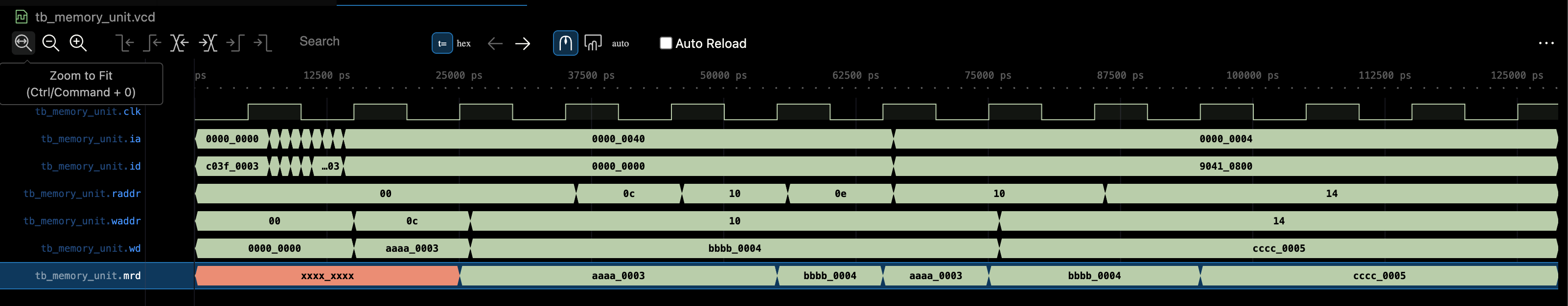
Few things to note:
- Read data comes out one cycle later after address
ia/raddr/waddris given - Writing to data memory is only done when or
weis high - Data memory was initially “empty” (giving out
x) - Memory data is able to produce what’s written, based on read address given by
raddr
Part A: PC Unit
PC Unit Schematic
Here is the suggested PC Unit schematic that you can implement. Take note of the input and output nodes. This will come in very useful when creating the module for your PC Unit.
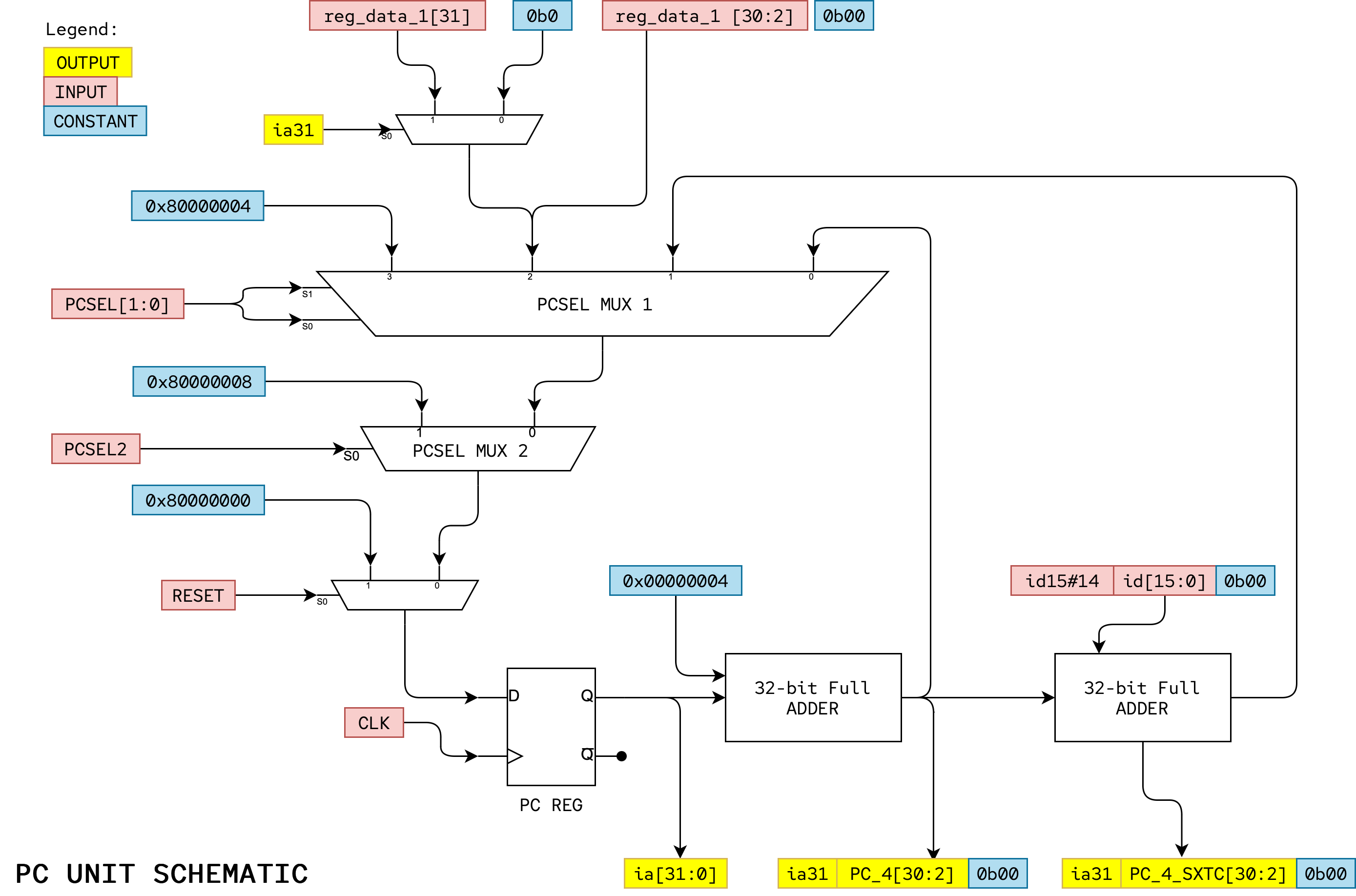
Here’s a suggested interface:
module pc_unit (
    input clk,
    input rst,
    input slowclk,
    input [15:0] id,
    input [2:0] pcsel,
    input [31:0] reg_data_1,
    output [31:0] pc_4,
    output [31:0] pc_4_sxtc,
    output [31:0] pcsel_out,
    output [31:0] ia
);
Task 1: PCSEL Multiplexers
The 32-bit 5-to-1 PC MUX selects the value to be loaded into the PC register at the next rising edge of the clock depending on the PCSEL control signal.
However, later on we might want to only advance the pc when some slowclk signal is 1 for manual debugging. You should take into account this aspect when building the PCSEL MUX.
XAddr and ILLOP
XAddr and ILLOP in the Beta diagram in our lecture notes represents constant addresses used when the Beta services an interrupt (triggered by IRQ) or executes an instruction with an illegal or unimplemented opcode. For this assignment assume that XAddr = 0x80000008 and ILLOP = 0x80000004 and we will make sure the first three locations of main memory contain BR instructions that branch to code which handle reset, illegal instruction traps and interrupts respectively. In other words, the first three locations of main memory contain:
Mem[0x80000000] = BR(reset_handler)
Mem[0x80000004] = BR(illop_handler)
Mem[0x80000008] = BR(interrupt_handler)
Lower Two Bits of PC
You also have to force the lower two bits of inputs going into the PC+4, PC+4+4*SXTC, and JT port of the MUX to be b00 because the memory is byte addressable but the Beta obtains one word of data/instructions at each clock cycle. You can do this with appropriate wiring using simple concatenation:
Example:
pc_d = {pcsel_out[31:2], 2'b00};
Task 2: RESET Multiplexer
Remember that we need to add a way to set the PC to zero on RESET. We use a two-input 32-bit MUX that selects 0x80000000 when the RESET signal is asserted, and the output of the PCSEL MUX when RESET is not asserted.
We shall use the RESET signal to force the PC to zero during the Beta CPU “startup” later on.
Task 3: 32-bit PC Reg
The PC is a separate 32-bit register that can be built using the register component mentioned in the previous lab.
Task 4: Increment-by-4
Conceptually, the increment-by-4 circuit is just a 32-bit adder with one input wired to the constant 4. It is possible to build a much smaller circuit if you design an adder optimized knowing that one of its inputs is 0x00000004 constant. In Verilog, you can directly concatenate the MSB of pc_q and add the remaining bits by 4 using the + operator.
Task 4: Shift-and-add
The branch-offset adder adds PC+4 to the 16-bit offset encoded in the instruction data id[15:0]. The offset is sign-extended to 32-bits and multiplied by 4 in preparation for the addition. Both the sign extension and shift operations can be done with appropriate wiring—no gates required.
  // compute sign extended C then multiply by 4, add this to PC + 4 later on
  wire [31:0] sxtc_x4 = ({ {16{id[15]} }, id[15:0]}) << 2;
Task 5: Supervisor Bit
The highest-order bit of the PC (PC31/ia31) is dedicated as the supervisor bit (see section 6.3 of the Beta Documentation).
- The
LDRinstruction ignores this bit, treating it as if it were zero. - The
JMPinstruction is allowed to clear the Supervisor bit or leave it unchanged, but cannot set it, - No other instructions may have any effect on
PC31
Setting the Supervisor Bit
Only
RESET,exceptions(ILLOP) andinterrupts(XAddr) cause the Supervisor bit of the BetaPCto become set.
This has the following three implications for your PC unit design:
-
0x80000000,0x80000004and0x80000008are loaded into the PC duringreset,ILLOPandIRQrespectively. This is the only way that the supervisor bit gets set. Note that afterresetthe Beta starts execution in supervisor mode. This is equivalent to when a regular computer is starting up. -
Bit 31 of the
PC+4and branch-offset inputs to the PCSEL MUX should be connected to the highest bit of the PC Reg output,ia31; i.e., the value of the supervisor bit doesn’t change when executing most instructions. -
You need to add additional logic to bit 31 of the
JTinput to the PCSEL MUX to ensure that JMP instruction can only clear or leave the supervisor bit unchanged. Here’s a table showing the new value of the supervisor bit after aJMPas function of JT31 and the current value of the supervisor bit (PC31):
| old PC31 (ia31) | JT31 (ra31) | new PC31 |
|---|---|---|
| 0 | – | 0 |
| 1 | 0 | 0 |
| 1 | 1 | 1 |
Testbench
Assuming you used the interface above, you can use this tb:
`timescale 1ns / 1ps

module tb_pc_unit;

  // -----------------------
  // DUT inputs
  // -----------------------
  reg         clk;
  reg         rst;
  reg         slowclk;
  reg  [15:0] id;
  reg  [ 2:0] pcsel;
  reg  [31:0] reg_data_1;

  // -----------------------
  // DUT outputs
  // -----------------------
  wire [31:0] pc_4;
  wire [31:0] pc_4_sxtc;
  wire [31:0] pcsel_out;
  wire [31:0] ia;

  // -----------------------
  // Instantiate DUT
  // -----------------------
  pc_unit dut (
      .clk(clk),
      .rst(rst),
      .slowclk(slowclk),
      .id(id),
      .pcsel(pcsel),
      .reg_data_1(reg_data_1),
      .pc_4(pc_4),
      .pc_4_sxtc(pc_4_sxtc),
      .pcsel_out(pcsel_out),
      .ia(ia)
  );

  // -----------------------
  // Clock gen: 100 MHz (10ns period)
  // -----------------------
  initial clk = 1'b0;
  always #5 clk = ~clk;

  // -----------------------
  // Helpers
  // -----------------------
  function [31:0] sxtc_x4;
    input [15:0] imm;
    begin
      sxtc_x4 = { {16{imm[15]} }, imm} << 2;
    end
  endfunction

  function [31:0] protect_msb;
    input [31:0] old_pc;
    input [31:0] candidate;
    begin
      protect_msb = {old_pc[31], candidate[30:0]};
    end
  endfunction

  task expect32;
    input [1023:0] tag;
    input [31:0] got;
    input [31:0] exp;
    begin
      if (got !== exp) begin
        $display("FAIL: %s got=%h exp=%h @ t=%0t", tag, got, exp, $time);
        $fatal(1);
      end else begin
        $display("PASS: %s = %h @ t=%0t", tag, got, $time);
      end
    end
  endtask

  task expect_align00;
    input [1023:0] tag;
    input [31:0] val;
    begin
      if (val[1:0] !== 2'b00) begin
        $display("FAIL: %s alignment violated val=%h @ t=%0t", tag, val, $time);
        $fatal(1);
      end else begin
        $display("PASS: %s aligned val=%h @ t=%0t", tag, val, $time);
      end
    end
  endtask

  // Pulse slowclk high across a rising edge so the PC register loads the mux output.
  task pc_load_once;
    begin
      @(negedge clk);
      slowclk = 1'b1;
      @(posedge clk);
      #1;
      slowclk = 1'b0;
    end
  endtask

  task wait_cycles(input integer n);
    integer k;
    begin
      for (k = 0; k < n; k = k + 1) @(posedge clk);
      #1;
    end
  endtask

  // Convenience: force a JMP load to a given reg_data_1 value
  task do_jmp_to(input [31:0] target);
    begin
      pcsel = 3'b010;
      reg_data_1 = target;
      #1;
      pc_load_once();
    end
  endtask

  // Convenience: do a branch load with a given immediate
  task do_branch(input [15:0] imm);
    begin
      pcsel = 3'b001;
      id = imm;
      #1;
      pc_load_once();
    end
  endtask

  // -----------------------
  // Wave dump
  // -----------------------
  initial begin
    $dumpfile("tb_pc_unit.vcd");
    $dumpvars(0, tb_pc_unit);
  end

  // -----------------------
  // Main test
  // -----------------------
  initial begin
    // defaults
    rst        = 1'b0;
    slowclk    = 1'b0;
    id         = 16'h0000;
    pcsel      = 3'b000;
    reg_data_1 = 32'h0000_0000;

    // -----------------------
    // Reset: PC reg reset value is 0x8000_0000 per register instantiation
    // -----------------------
    @(negedge clk);
    rst = 1'b1;
    wait_cycles(2);
    rst = 1'b0;
    wait_cycles(1);

    expect32("After reset, ia", ia, 32'h8000_0000);

    // -----------------------
    // PC+4 increment a bit
    // -----------------------
    pcsel = 3'b000;
    pc_load_once();
    expect32("PC+4 #1 ia", ia, 32'h8000_0004);

    pc_load_once();
    expect32("PC+4 #2 ia", ia, 32'h8000_0008);

    // -----------------------
    // IRQ vector: pcsel=100 then load => 0x8000_0008
    // -----------------------
    pcsel = 3'b100;
    pc_load_once();
    expect32("IRQ load ia", ia, 32'h8000_0008);

    // =========================================================================
    // BRANCH: bigger address, then branch back to lower address
    // =========================================================================

    // Put PC at 0x8000_0010
    pcsel = 3'b000;
    pc_load_once();  // 0x8000_000C
    pc_load_once();  // 0x8000_0010
    expect32("Setup PC=0x80000010", ia, 32'h8000_0010);

    // Branch forward by +100 (id=0x0064) => +400 bytes
    // target = protect(old_pc, (old_pc+4) + (sxtc<<2))
    begin : branch_forward_big
      reg [31:0] old_pc, exp_pc4, exp_raw, exp_prot, exp_aligned;
      old_pc = ia;
      exp_pc4 = old_pc + 32'd4;
      exp_raw = exp_pc4 + sxtc_x4(16'h0064);
      exp_prot = protect_msb(old_pc, exp_raw);
      exp_aligned = {exp_prot[31:2], 2'b00};

      pcsel = 3'b001;
      id = 16'h0064;
      #1;
      expect32("branch(+100): pc_4_sxtc combinational", pc_4_sxtc, exp_prot);
      pc_load_once();
      expect32("branch(+100): ia after load", ia, exp_aligned);
      expect_align00("branch(+100): ia alignment", ia);
    end

    // Branch back by -60 (id=0xFFC4) => -240 bytes
    begin : branch_back_lower
      reg [31:0] old_pc, exp_pc4, exp_raw, exp_prot, exp_aligned;
      old_pc = ia;
      exp_pc4 = old_pc + 32'd4;
      exp_raw = exp_pc4 + sxtc_x4(16'hFFC4);  // -60 * 4
      exp_prot = protect_msb(old_pc, exp_raw);
      exp_aligned = {exp_prot[31:2], 2'b00};

      pcsel = 3'b001;
      id = 16'hFFC4;
      #1;
      expect32("branch(-60): pc_4_sxtc combinational", pc_4_sxtc, exp_prot);
      pc_load_once();
      expect32("branch(-60): ia after load", ia, exp_aligned);
      expect_align00("branch(-60): ia alignment", ia);
    end

    // =========================================================================
    // BRANCH that would flip MSB if NOT protected (crossing 0x7FFF_FFFF -> 0x8000_0000)
    // We do:
    //   1) JMP to 0x7FFF_FFF0 while old PC MSB is 1 so JMP clears MSB to 0
    //   2) Branch forward with small positive offset that would raw-cross to 0x8000_0xxx
    //      but protection must keep MSB=0, so it becomes 0x0000_0xxx
    // =========================================================================

    // Step 1: make PC MSB become 0 by JMP to 0x7FFF_FFF0.
    // old_pc[31]=1, reg_data_1[31]=0 => AND => 0, so MSB cleared.
    do_jmp_to(32'h7FFF_FFF0);
    expect32("JMP to 0x7FFFFFF0 should clear MSB (PC becomes 0x7FFFFFF0)", ia, 32'h7FFF_FFF0);
    expect_align00("JMP 0x7FFFFFF0 alignment", ia);

    // Step 2: choose id so raw target crosses into 0x8000_xxxx.
    // old_pc=0x7FFF_FFF0
    // pc+4 = 0x7FFF_FFF4
    // want pc+4 + offset = 0x8000_0004 (raw) => offset = +0x0010 (16 bytes) => imm=4
    begin : branch_cross_msb_protection
      reg [31:0] old_pc, exp_pc4, exp_raw, exp_prot, exp_aligned;
      old_pc = ia;  // 0x7FFF_FFF0
      exp_pc4 = old_pc + 32'd4;  // 0x7FFF_FFF4
      exp_raw = exp_pc4 + sxtc_x4(16'h0004);  // +16 => 0x8000_0004 (raw)
      // protection must keep MSB=0 (old_pc[31]=0), so expected is 0x0000_0004
      exp_prot = protect_msb(old_pc, exp_raw);
      exp_aligned = {exp_prot[31:2], 2'b00};

      pcsel = 3'b001;
      id = 16'h0004;
      #1;
      expect32("branch(cross): raw would be 0x80000004, protected pc_4_sxtc", pc_4_sxtc, exp_prot);
      pc_load_once();
      expect32("branch(cross): ia after load should keep MSB=0", ia, exp_aligned);
      expect_align00("branch(cross): ia alignment", ia);

      // Extra explicit check of the expected literal in this scenario
      expect32("branch(cross): expected literal ia", ia, 32'h0000_0004);
    end

    // =========================================================================
    // JMP MSB behavior when PC31 is 0:
    // Once PC31=0, JMP to 0x8000_001C should become 0x0000_001C
    // because (old_pc[31] & reg_data_1[31]) = 0 & 1 = 0.
    // =========================================================================

    // Ensure PC31=0 already (it is from previous branch).
    if (ia[31] !== 1'b0) begin
      $display("FAIL: expected PC31=0 before JMP MSB test, ia=%h @ t=%0t", ia, $time);
      $fatal(1);
    end

    begin : jmp_msb_clear_when_pc31_zero
      reg [31:0] old_pc, exp_out, exp_aligned;
      old_pc = ia;  // MSB 0
      pcsel = 3'b010;
      reg_data_1 = 32'h8000_001C;  // MSB 1
      #1;

      exp_out = {(old_pc[31] & reg_data_1[31]), reg_data_1[30:0]};  // should be 0x0000_001C
      exp_aligned = {exp_out[31:2], 2'b00};

      expect32("jmp(PC31=0, target=0x8000001C): pcsel_out combinational", pcsel_out, exp_out);
      pc_load_once();
      expect32("jmp(PC31=0): ia after load should be 0x0000001C", ia, exp_aligned);
      expect32("jmp(PC31=0): expected literal ia", ia, 32'h0000_001C);
      expect_align00("jmp(PC31=0): ia alignment", ia);
    end

    // =========================================================================
    // JMP that would set MSB to 1 only if allowed.
    // With PC31=0, even if reg_data_1[31]=1, MSB must stay 0.
    // With PC31=1, reg_data_1[31]=1, MSB stays 1.
    // =========================================================================

    // Case A: PC31=0, reg_data_1[31]=1 -> stays 0
    do_jmp_to(32'hFFFF_FFFC);  // reg_data_1[31]=1 but AND with old_pc[31]=0 => MSB=0
    expect32("JMP with PC31=0 to 0xFFFFFFFC should still clear MSB", ia, 32'h7FFF_FFFC);
    // Explanation for the literal above:
    // pcsel_out = {0 & 1, reg_data_1[30:0]} = {0, 0x7FFF_FFFC} = 0x7FFF_FFFC
    expect_align00("JMP to 0x7FFFFFFC alignment", ia);

    // Case B: Force PC31=1 again via IRQ vector, then JMP with reg_data_1[31]=1 keeps MSB=1
    pcsel = 3'b100;
    pc_load_once();
    expect32("IRQ again sets PC MSB=1", ia, 32'h8000_0008);

    begin : jmp_keep_msb_when_pc31_one
      reg [31:0] old_pc, exp_out;
      old_pc = ia;  // MSB 1
      pcsel = 3'b010;
      reg_data_1 = 32'h9000_0011;  // MSB 1, unaligned low bits
      #1;

      exp_out = {(old_pc[31] & reg_data_1[31]), reg_data_1[30:0]};  // MSB stays 1
      pc_load_once();
      expect32("jmp(PC31=1,target msb=1): ia aligned", ia, {exp_out[31:2], 2'b00});
      expect_align00("jmp(PC31=1): ia alignment", ia);
    end

    $display("ALL TESTS PASSED");
    $finish;
  end

endmodule
If all works well, you should get the following waveform and message:
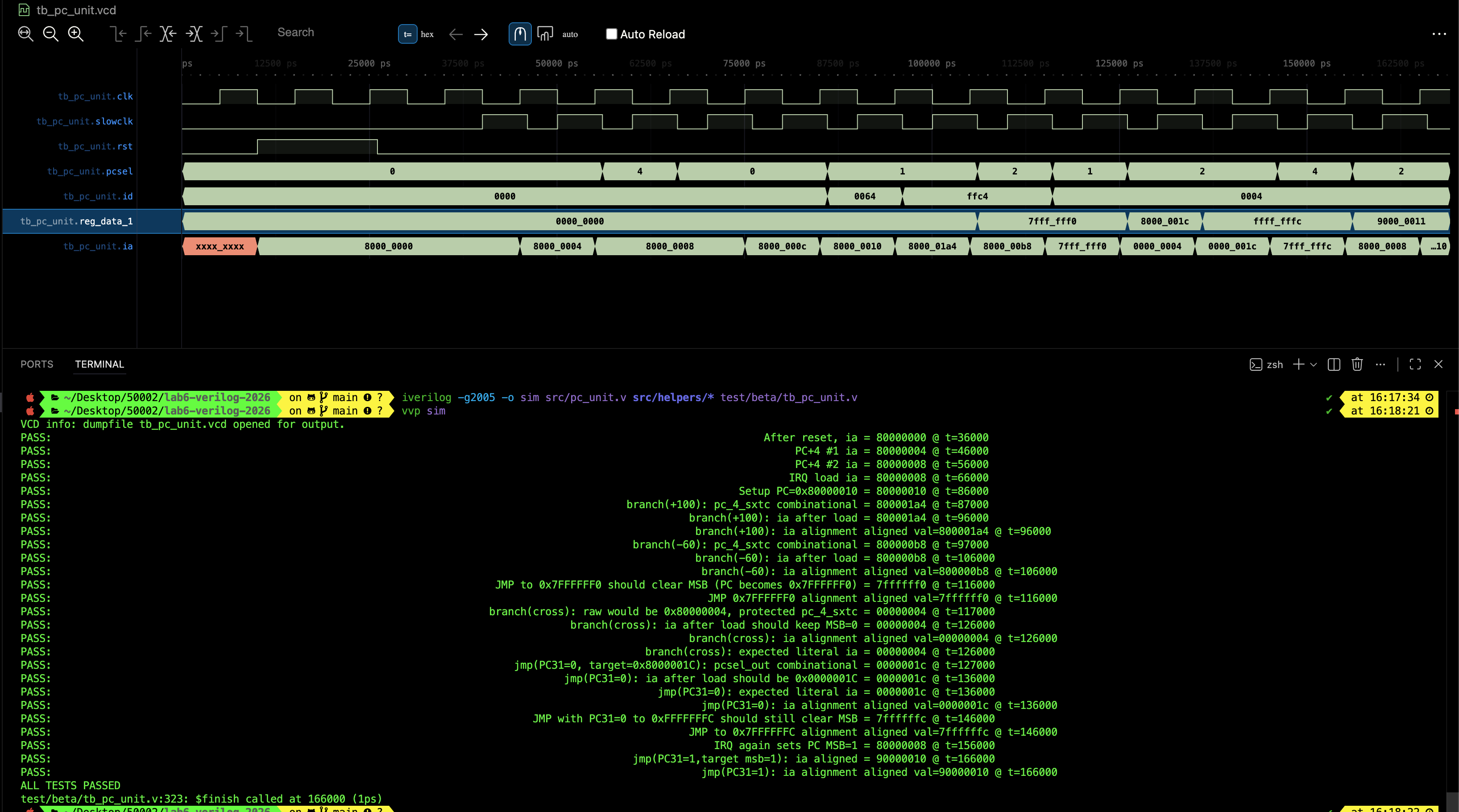
The testbench is design to test the following critical scenarios:
- Test RESET, IRQ, and ILLOP cases
- Test JMP, BEQ/BNE cases (both + and - memory addresses)
- PC31 protection (Cleared via JMP, attempt to set via JMP, and BNE/BEQ)
Part B: REGFILE Unit
REGFILE Unit Schematic
Here is the suggested REGFILE Unit schematic that you can implement.
This unit utilises regfile_memory.
The suggested interface for regfile_unit.v is:
module regfile_unit (
    input clk,
    input rst,
    input [4:0] ra,
    input [4:0] rb,
    input [4:0] rc,
    input wasel,
    input ra2sel,
    input werf,
    input [31:0] wdsel_out,
    input slowclk,
    output z,
    output [31:0] rd1,
    output [31:0] rd2,
    output [31:0] mwd
);
Task 6: RA2SEL and WASEL Mux
You will need a MUX controlled by RA2SEL to select the correct address for the B read port. The 5-bit 2-to-1 WASEL multiplexer determines the write address for the register file.
Task 7: Regfile Memory
The register file is a 3-port memory. It should be implemented in regfile_memory.v, which is then utilised by regfile_unit.luc.
The RD1 port output producing reg_data_1[31:0] is also wired directly as the third (for JMP) input of the PCSEL multiplexer. Remember we already force the low-order two bits to zero and to add supervisor bit logic to bit 31 in the PCSEL Unit, so we do not have to do it here anymore.
Here’s a suggested interface:
module regfile_memory (
    input clk,
    input rst,
    input [4:0] ra1,
    input [4:0] ra2,
    input [4:0] wa,
    input [31:0] wd,
    input we,
    output [31:0] rd1,
    output [31:0] rd2
);
Testbench for Regfile Memory
And you can use the following testbench:
`timescale 1ns / 1ps

module tb_regfile_memory;

  // --------------------------------------------------------------------------
  // DUT I/O (Verilog-2005 style)
  // --------------------------------------------------------------------------
  reg clk;
  reg rst;
  reg [4:0] ra1, ra2, wa;
  reg [31:0] wd;
  reg        we;
  wire [31:0] rd1, rd2;

  regfile_memory dut (
      .clk(clk),
      .rst(rst),
      .ra1(ra1),
      .ra2(ra2),
      .wa (wa),
      .wd (wd),
      .we (we),
      .rd1(rd1),
      .rd2(rd2)
  );

  // --------------------------------------------------------------------------
  // Clock
  // --------------------------------------------------------------------------
  initial begin
    clk = 1'b0;
    forever #5 clk = ~clk;
  end

  // --------------------------------------------------------------------------
  // Waveform
  // --------------------------------------------------------------------------
  initial begin
    $dumpfile("regfile_memory_tb.vcd");
    $dumpvars(0, tb_regfile_memory);
  end

  // --------------------------------------------------------------------------
  // Simple expected model (R31 always 0)
  // --------------------------------------------------------------------------
  reg [31:0] exp[0:31];
  integer i;

  task exp_reset;
    begin
      for (i = 0; i < 32; i = i + 1) exp[i] = 32'b0;
      exp[31] = 32'b0;
    end
  endtask

  task exp_write;
    input [4:0] waddr;
    input [31:0] wdata;
    input wen;
    begin
      if (wen && (waddr != 5'd31)) exp[waddr] = wdata;
      exp[31] = 32'b0;
    end
  endtask

  // --------------------------------------------------------------------------
  // Helpers
  // --------------------------------------------------------------------------
  task read_check;
    input [4:0] a1;
    input [4:0] a2;
    begin
      ra1 = a1;
      ra2 = a2;
      #1;  // settle combinational read

      if (rd1 !== exp[a1]) begin
        $display("FAIL rd1: ra1=%0d got=%h exp=%h time=%0t", a1, rd1, exp[a1], $time);
        $fatal;
      end
      if (rd2 !== exp[a2]) begin
        $display("FAIL rd2: ra2=%0d got=%h exp=%h time=%0t", a2, rd2, exp[a2], $time);
        $fatal;
      end
    end
  endtask

  task do_write;
    input [4:0] waddr;
    input [31:0] wdata;
    begin
      // setup before posedge
      wa = waddr;
      wd = wdata;
      we = 1'b1;

      @(posedge clk);
      exp_write(waddr, wdata, 1'b1);

      #1;
      we = 1'b0;
    end
  endtask

  // Same-cycle write+read expectation for THIS regfile:
  // - before posedge: read shows OLD value
  // - after posedge: read shows NEW value
  task write_read_same_cycle_check;
    input [4:0] r;
    input [31:0] new_data;
    reg [31:0] old_data;
    begin
      old_data = exp[r];

      // set read + write same register
      ra1 = r;
      ra2 = r;
      wa = r;
      wd = new_data;
      we = 1'b1;

      // before edge: old
      #1;
      if (rd1 !== old_data) begin
        $display("FAIL same-cycle pre-edge: r=%0d got=%h exp(old)=%h time=%0t", r, rd1, old_data,
                 $time);
        $fatal;
      end

      @(posedge clk);
      exp_write(r, new_data, 1'b1);

      // after edge: new
      #1;
      if (rd1 !== exp[r]) begin
        $display("FAIL same-cycle post-edge: r=%0d got=%h exp(new)=%h time=%0t", r, rd1, exp[r],
                 $time);
        $fatal;
      end

      we = 1'b0;
    end
  endtask

  task apply_reset;
    begin
      we  = 1'b0;
      wa  = 5'd0;
      wd  = 32'd0;
      ra1 = 5'd0;
      ra2 = 5'd0;

      rst = 1'b1;
      exp_reset();

      @(posedge clk);
      @(posedge clk);
      rst = 1'b0;

      #1;
      read_check(5'd0, 5'd31);
    end
  endtask

  // --------------------------------------------------------------------------
  // Main
  // --------------------------------------------------------------------------
  initial begin
    rst = 1'b0;
    we  = 1'b0;
    wa  = 5'd0;
    wd  = 32'd0;
    ra1 = 5'd0;
    ra2 = 5'd0;
    exp_reset();

    apply_reset();

    // Write to R1, R5, R30, R31
    do_write(5'd1, 32'h1111_0001);
    do_write(5'd5, 32'h5555_0005);
    do_write(5'd30, 32'h3030_0030);
    do_write(5'd31, 32'hDEAD_BEEF);  // ignored

    // Check outputs in the next cycle (reads are combinational)
    read_check(5'd1, 5'd5);
    read_check(5'd30, 5'd31);
    read_check(5'd31, 5'd31);

    // Write and read "same cycle" to R5: old before posedge, new after posedge
    write_read_same_cycle_check(5'd5, 32'hAAAA_0005);

    // Read back R5 and something else
    read_check(5'd5, 5'd1);

    // Extra coverage
    do_write(5'd0, 32'h0000_1234);
    do_write(5'd10, 32'h1010_1010);
    do_write(5'd29, 32'h2929_2929);
    do_write(5'd31, 32'hFFFF_FFFF);  // still ignored
    read_check(5'd0, 5'd10);
    read_check(5'd29, 5'd31);

    $display("PASS: all regfile_memory tests completed.");
    $finish;
  end

endmodule
Testbench waveform:
- To ensure that
R31is always0despite attempts to write to it - Read and write in the same cycle update the registers accordingly, no
zoutput observed
Task 8: Z Logic
Z logic can be added to the output of the RD1 port of the register file memory above. The value of Z must be 1 if and only if reg_data_1[31:0] is 0x00000000. Z must be 0 otherwise. This is exactly a NOR logic. You can create a reduction NOR logic gate very easily in Lucid and Verilog, but you’re welcome to follow the schematic above.
Task 9: mwd[31:0] Output
Finally, we need to connect the output of the RD2 port of the register file memory above to produce mwd[31:0].
Testbench
Here’s a testbench to get you started:
`timescale 1ns / 1ps

module tb_regfile_unit;

  // --------------------------------------------------------------------------
  // DUT I/O
  // --------------------------------------------------------------------------
  reg clk;
  reg rst;
  reg [4:0] ra, rb, rc;
  reg         wasel;
  reg         ra2sel;
  reg         werf;
  reg  [31:0] wdsel_out;
  reg         slowclk;

  wire        z;
  wire [31:0] rd1;
  wire [31:0] rd2;
  wire [31:0] mwd;

  regfile_unit dut (
      .clk(clk),
      .rst(rst),
      .ra(ra),
      .rb(rb),
      .rc(rc),
      .wasel(wasel),
      .ra2sel(ra2sel),
      .werf(werf),
      .wdsel_out(wdsel_out),
      .slowclk(slowclk),
      .z(z),
      .rd1(rd1),
      .rd2(rd2),
      .mwd(mwd)
  );

  // --------------------------------------------------------------------------
  // Clock
  // --------------------------------------------------------------------------
  initial begin
    clk = 1'b0;
    forever #5 clk = ~clk;
  end

  // --------------------------------------------------------------------------
  // Waveform
  // --------------------------------------------------------------------------
  initial begin
    $dumpfile("regfile_unit_tb.vcd");
    $dumpvars(0, tb_regfile_unit);
  end

  // --------------------------------------------------------------------------
  // Expected regfile model (matches regfile_memory: R31 hardwired 0)
  // --------------------------------------------------------------------------
  reg [31:0] exp[0:31];
  integer i;

  task exp_reset;
    begin
      for (i = 0; i < 32; i = i + 1) exp[i] = 32'b0;
      exp[31] = 32'b0;
    end
  endtask

  task exp_write;
    input [4:0] waddr;
    input [31:0] wdata;
    input wen;
    begin
      if (wen && (waddr != 5'd31)) exp[waddr] = wdata;
      exp[31] = 32'b0;
    end
  endtask

  // --------------------------------------------------------------------------
  // Effective address functions (like DUT)
  // --------------------------------------------------------------------------
  function [4:0] eff_wa;
    input [4:0] rc_in;
    input wasel_in;
    begin
      eff_wa = wasel_in ? 5'd30 : rc_in;
    end
  endfunction

  function [4:0] eff_ra2;
    input [4:0] rb_in;
    input [4:0] rc_in;
    input ra2sel_in;
    begin
      eff_ra2 = ra2sel_in ? rc_in : rb_in;
    end
  endfunction

  // w_werf inside DUT = slowclk & werf
  function eff_we;
    input slow_in;
    input werf_in;
    begin
      eff_we = slow_in & werf_in;
    end
  endfunction

  // --------------------------------------------------------------------------
  // Output checker
  // --------------------------------------------------------------------------
  task check_outputs;
    reg [ 4:0] a2;
    reg [31:0] exp_rd1;
    reg [31:0] exp_rd2;
    reg        exp_z;
    begin
      a2 = eff_ra2(rb, rc, ra2sel);

      exp_rd1 = exp[ra];
      exp_rd2 = exp[a2];
      exp_z = (exp_rd1 == 32'b0);

      #1;  // settle combinational paths

      if (rd1 !== exp_rd1) begin
        $display("FAIL rd1: ra=%0d got=%h exp=%h time=%0t", ra, rd1, exp_rd1, $time);
        $fatal;
      end
      if (rd2 !== exp_rd2) begin
        $display("FAIL rd2: ra2=%0d got=%h exp=%h time=%0t", a2, rd2, exp_rd2, $time);
        $fatal;
      end
      if (mwd !== exp_rd2) begin
        $display("FAIL mwd: expected mirror of rd2. got=%h exp=%h time=%0t", mwd, exp_rd2, $time);
        $fatal;
      end
      if (z !== exp_z) begin
        $display("FAIL z: got=%b exp=%b (rd1 exp=%h) time=%0t", z, exp_z, exp_rd1, $time);
        $fatal;
      end
    end
  endtask

  // --------------------------------------------------------------------------
  // Reset helper
  // --------------------------------------------------------------------------
  task apply_reset;
    begin
      ra = 5'd0;
      rb = 5'd0;
      rc = 5'd0;
      wasel = 1'b0;
      ra2sel = 1'b0;
      werf = 1'b0;
      wdsel_out = 32'd0;
      slowclk = 1'b1;  // default "always enabled" for basic tests

      rst = 1'b1;
      exp_reset();

      @(posedge clk);
      @(posedge clk);
      rst = 1'b0;

      check_outputs();  // all zero, z should be 1
    end
  endtask

  // --------------------------------------------------------------------------
  // Perform a "write attempt" for one clk edge with current control signals.
  // Update expected only if (slowclk & werf) is 1 at the edge.
  // --------------------------------------------------------------------------
  task do_write_attempt_one_edge;
    input [31:0] wdata;
    reg [4:0] waddr;
    reg       wen;
    begin
      wdsel_out = wdata;

      // Drive werf high for this attempt
      werf = 1'b1;

      waddr = eff_wa(rc, wasel);
      wen = eff_we(slowclk, werf);

      @(posedge clk);
      exp_write(waddr, wdata, wen);

      #1;
      werf = 1'b0;
    end
  endtask

  // --------------------------------------------------------------------------
  // Same-cycle write+read check (no bypass):
  // old before posedge, new after posedge, but only if gated we is 1.
  // --------------------------------------------------------------------------
  task write_read_same_cycle_check;
    input [4:0] target_reg;
    input [31:0] new_data;
    input expect_write;  // 1 if slowclk&werf will be 1 at posedge
    reg [31:0] old_data;
    reg [ 4:0] waddr;
    reg        wen;
    begin
      old_data = exp[target_reg];

      // Arrange write address = target_reg
      if (target_reg == 5'd30) begin
        wasel = 1'b1;
        rc = 5'd7;
      end else begin
        wasel = 1'b0;
        rc = target_reg;
      end

      // Read rd1 from same target
      ra = target_reg;

      wdsel_out = new_data;
      werf = 1'b1;

      // Pre-edge: old value
      #1;
      if (rd1 !== old_data) begin
        $display("FAIL same-cycle pre-edge: r=%0d got=%h exp(old)=%h time=%0t", target_reg, rd1,
                 old_data, $time);
        $fatal;
      end

      // Edge: update expected depending on gated write enable
      waddr = eff_wa(rc, wasel);
      wen   = eff_we(slowclk, werf);

      @(posedge clk);
      exp_write(waddr, new_data, wen);

      // Post-edge: should be new only if write happened
      #1;
      if (expect_write) begin
        if (rd1 !== exp[target_reg]) begin
          $display("FAIL same-cycle post-edge (expected write): r=%0d got=%h exp(new)=%h time=%0t",
                   target_reg, rd1, exp[target_reg], $time);
          $fatal;
        end
      end else begin
        if (rd1 !== old_data) begin
          $display(
              "FAIL same-cycle post-edge (expected NO write): r=%0d got=%h exp(still old)=%h time=%0t",
              target_reg, rd1, old_data, $time);
          $fatal;
        end
      end

      werf = 1'b0;
    end
  endtask

  // --------------------------------------------------------------------------
  // Main test sequence
  // --------------------------------------------------------------------------
  initial begin
    // init
    rst = 1'b0;
    ra = 5'd0;
    rb = 5'd0;
    rc = 5'd0;
    wasel = 1'b0;
    ra2sel = 1'b0;
    werf = 1'b0;
    wdsel_out = 32'd0;
    slowclk = 1'b1;
    exp_reset();

    apply_reset();

    // ======================================================================
    // A) Basic tests with slowclk = 1 (gating disabled)
    // ======================================================================
    slowclk = 1'b1;

    // 1) Write to R1 via rc when wasel=0
    wasel = 1'b0;
    rc = 5'd1;
    do_write_attempt_one_edge(32'h1111_0001);

    // read back through rd1 and rd2 muxes
    ra = 5'd1;
    rb = 5'd0;
    ra2sel = 1'b0;  // rd2 from rb (R0)
    check_outputs();

    ra2sel = 1'b1;  // rd2 from rc (R1)
    check_outputs();

    // 2) Write to R5
    wasel = 1'b0;
    rc = 5'd5;
    do_write_attempt_one_edge(32'h5555_0005);

    ra     = 5'd5;  // rd1 nonzero => z=0
    rb     = 5'd1;  // rd2 from rb
    ra2sel = 1'b0;
    check_outputs();

    ra2sel = 1'b1;  // rd2 from rc (R5)
    check_outputs();

    // 3) wasel=1 forces write to R30
    wasel = 1'b1;
    rc = 5'd2;  // ignored for write addr
    do_write_attempt_one_edge(32'h3030_0030);

    ra = 5'd30;
    rb = 5'd0;
    ra2sel = 1'b0;
    check_outputs();

    // 4) Attempt write to R31 (should not change, always 0)
    wasel = 1'b0;
    rc = 5'd31;
    do_write_attempt_one_edge(32'hDEAD_BEEF);

    ra = 5'd31;     // rd1=0 => z=1
    rb = 5'd31;
    ra2sel = 1'b0;
    check_outputs();

    ra2sel = 1'b1;
    check_outputs();

    // 5) Same-cycle write+read to R5 with slowclk=1: should update at posedge
    write_read_same_cycle_check(5'd5, 32'hAAAA_0005, 1'b1);

    // ======================================================================
    // B) Gating tests: keep werf high, but writes only happen when slowclk=1
    // ======================================================================
    // Set up: target R10, read it via rd1
    wasel = 1'b0;
    rc = 5'd10;
    ra = 5'd10;
    rb = 5'd0;
    ra2sel = 1'b0;

    // Hold werf high across several cycles, toggle slowclk manually.
    werf = 1'b1;

    // B1) slowclk=0: write should NOT happen
    slowclk = 1'b0;
    wdsel_out = 32'h1010_1010;

    // pre-check current value (likely 0)
    check_outputs();

    @(posedge clk);
    // expected does NOT update because gated we = 0
    exp_write(eff_wa(rc, wasel), wdsel_out, eff_we(slowclk, werf));

    #1;
    check_outputs();  // still old value (no write)

    // B2) slowclk=1: write SHOULD happen on this edge
    slowclk   = 1'b1;
    wdsel_out = 32'h1010_1010;

    @(posedge clk);
    exp_write(eff_wa(rc, wasel), wdsel_out, eff_we(slowclk, werf));

    #1;
    check_outputs();  // now updated

    // B3) slowclk=0 again: no further change even if wdsel_out changes
    slowclk   = 1'b0;
    wdsel_out = 32'h2222_2222;

    @(posedge clk);
    exp_write(eff_wa(rc, wasel), wdsel_out, eff_we(slowclk, werf));

    #1;
    check_outputs();  // should remain 0x1010_1010

    // B4) slowclk=1 again: should update to new wdsel_out
    slowclk = 1'b1;

    @(posedge clk);
    exp_write(eff_wa(rc, wasel), wdsel_out, eff_we(slowclk, werf));

    #1;
    check_outputs();  // should become 0x2222_2222

    // stop holding werf
    werf = 1'b0;

    // Also do a same-cycle write+read check demonstrating gating:
    // slowclk=0 -> no update
    slowclk = 1'b0;
    write_read_same_cycle_check(5'd5, 32'hBBBB_0005, 1'b0);

    // slowclk=1 -> update
    slowclk = 1'b1;
    write_read_same_cycle_check(5'd5, 32'hCCCC_0005, 1'b1);

    $display("PASS: all regfile_unit tests completed (including slowclk gating).");
    $finish;
  end

endmodule
Things to note:
- When
ra2selis high, we are reading fromrcinstead ofrb - When
waselis high, we are writing toR30instead ofrc, so we need to read fromR30in the next cycle to confirm that - If
slowclkis low, then no writing operation happens
Part C: CONTROL Unit
CONTROL Unit Schematic
Here is the suggested CONTROL Unit schematic that you can implement.
Here’s a suggested interface:
module control_unit (
    input  wire       clk,
    input  wire       irq,
    input  wire       z,
    input  wire       rst,
    input  wire [5:0] opcode,
    input  wire       slowclk,
    input  wire       ia31,
    output reg  [2:0] pcsel,
    output reg        wasel,
    output reg        asel,
    output reg        ra2sel,
    output reg        bsel,
    output reg  [5:0] alufn,
    output reg  [1:0] wdsel,
    output reg        werf,
    output reg        wr
);
ROM
The control logic should be tailored to generate the control signals your logic requires, which may differ from what’s shown in the diagram above. Here’s a way to build such ROM in Verilog:
module cu_rom (
    input  wire [ 5:0] opcode,
    output wire [16:0] cw
);
  reg [16:0] rom[0:63];

  integer i;
  initial begin
    // default ILLOP for everything
    for (i = 0; i < 64; i = i + 1) rom[i] = 17'b01110000000000010;

    // override only the entries you listed
    rom[6'h3E] = 17'b00000011000110110;  // SRAC
    rom[6'h3D] = 17'b00000011000010110;  // SHRC
    rom[6'h3C] = 17'b00000011000000110;  // SHLC
    rom[6'h3A] = 17'b00000010101100110;  // XORC
    rom[6'h39] = 17'b00000010111100110;  // ORC
    rom[6'h38] = 17'b00000010110000110;  // ANDC
    rom[6'h36] = 17'b00000011101110110;  // CMPLEC
    rom[6'h35] = 17'b00000011101010110;  // CMPLTC
    rom[6'h34] = 17'b00000011100110110;  // CMPEQC
    rom[6'h31] = 17'b00000010000010110;  // SUBC
    rom[6'h30] = 17'b00000010000000110;  // ADDC

    rom[6'h2E] = 17'b00000001000110110;  // SRA
    rom[6'h2D] = 17'b00000001000010110;  // SHR
    rom[6'h2C] = 17'b00000001000000110;  // SHL
    rom[6'h2A] = 17'b00000000101100110;  // XOR
    rom[6'h29] = 17'b00000000111100110;  // OR
    rom[6'h28] = 17'b00000000110000110;  // AND
    rom[6'h26] = 17'b00000001101110110;  // CMPLE
    rom[6'h25] = 17'b00000001101010110;  // CMPLT
    rom[6'h24] = 17'b00000001100110110;  // CMPEQ
    rom[6'h21] = 17'b00000000000010110;  // SUB
    rom[6'h20] = 17'b00000000000000110;  // ADD

    rom[6'h1F] = 17'b00001000110101010;  // LDR
    rom[6'h1E] = 17'b00001000110100010;  // BNE
    rom[6'h1D] = 17'b00001000110100010;  // BEQ
    rom[6'h1B] = 17'b01001000110100010;  // JMP
    rom[6'h19] = 17'b00000110000000001;  // ST
    rom[6'h18] = 17'b00000010000001010;  // LD
  end

  assign cw = rom[opcode];
endmodule
This module is purely combinational, accepting 6 bits OPCODE and producing 17 bits control signal.
Some of the signals can connect directly to the appropriate logic, e.g., ALUFN[5:0] can connect directly to the ALUFN inputs of your ALU, however some signals like PCSEL[2:0] requires some degree of post-processing depending on the value of other signals like Z.
If you need to implement MUL or DIV in your Beta CPU, please modify the ROM yourself.
For this lab, further processing for control signals: PCSEL, wasel, wdsel, werf, wr are needed, let’s do this.
WR and WERF
We do need to be careful with the write enable signal for main memory (WR) which needs to be valid even before the first instruction is fetched from memory. WR is an input to the main memory, and recall that ALL inputs need to be VALID (0 is also a valid value!) in order for the main memory to give a valid output data. You should include some additional logic that forces wr to b0 when reset is 1. This takes highest priority, hence it is written at the bottom of the always block in control_unit.luc.
Task 10: PCSEL
The PCSEL logic should take into account the presence of branching BNE/BEQ OPCODE, and output the correct signal depending on the value of Z if branching is indeed happening. Here’s the related OPCODE and PCSEL value:
| OPCODE | Z | PCSEL |
|---|---|---|
BEQ 011101 |
0 | 000 |
BEQ 011101 |
1 | 001 |
BNE 011110 |
0 | 001 |
BNE 011110 |
1 | 000 |
If you are using purely a ROM-based implementation without additional logic (128 words in the ROM as opposed to just 64), you can make Z an additional address input to the ROM (doubling its size). A better implementation shall use external logic to modify the value of the PCSEL signals as defined in our schematic above.
Task 11: IRQ Handling
When IRQ signal is 1 and the Beta is in “user mode” (PC31 is zero), an interrupt should occur. Asserting IRQ should have NO effect when in “supervisor mode” (PC31 is one). You should add logic that causes the Beta to abort the current instruction and save the current PC+4 in register XP (11110) and to set the PC to 0x80000008.
In other words, an interrupt event forces the following control signals regardless of the current instruction:
- PCSEL to
b100(select0x80000008as the nextPCvalue) - WASEL to
b1(selectXPas the register file write address) - WERF to
b1(write into the register file) - WDSEL to
b00(selectPC+4as the data to be written into the register file) - WR to
b0(this ensures that if the interrupted instruction was aSTthat it doesn’t get to write into main memory).
Note that you’ll also want to add logic to reset the Beta; at the very least when reset is asserted you’ll need to force the PC to 0x80000000 and ensure that WR is 0 (to prevent your initialized main memory from being overwritten).
Testbench
You can run this tb:
`timescale 1ns / 1ps

module tb_control_unit;

  // DUT inputs
  reg        clk;
  reg        irq;
  reg        z;
  reg        rst;
  reg  [5:0] opcode;
  reg        slowclk;
  reg        ia31;

  // DUT outputs
  wire [2:0] pcsel;
  wire       wasel;
  wire       asel;
  wire       ra2sel;
  wire       bsel;
  wire [5:0] alufn;
  wire [1:0] wdsel;
  wire       werf;
  wire       wr;

  // Instantiate DUT
  control_unit dut (
      .clk(clk),
      .irq(irq),
      .z(z),
      .rst(rst),
      .opcode(opcode),
      .slowclk(slowclk),
      .ia31(ia31),
      .pcsel(pcsel),
      .wasel(wasel),
      .asel(asel),
      .ra2sel(ra2sel),
      .bsel(bsel),
      .alufn(alufn),
      .wdsel(wdsel),
      .werf(werf),
      .wr(wr)
  );

  // ==========
  // Clocking
  // ==========
  initial clk = 1'b0;
  always #5 clk = ~clk;

  // ==========
  // Helpers
  // ==========
  task tick;
    begin
      @(negedge clk);
      @(posedge clk);
      #1;
    end
  endtask

  task apply_inputs;
    input [5:0] op;
    input z_in;
    input irq_in;
    input slow_in;
    input ia31_in;
    begin
      opcode  = op;
      z       = z_in;
      irq     = irq_in;
      slowclk = slow_in;
      ia31    = ia31_in;
      #1;
    end
  endtask

  task fail;
    input [255:0] msg;
    begin
      $display("FAIL: %0s", msg);
      $stop;  // pause for debug
      $finish;  // end if continued
    end
  endtask

  task expect_ctrl;
    input [2:0] exp_pcsel;
    input exp_wasel;
    input exp_asel;
    input exp_ra2sel;
    input exp_bsel;
    input [5:0] exp_alufn;
    input [1:0] exp_wdsel;
    input exp_werf;
    input exp_wr;
    input [255:0] tag;
    begin
      if (pcsel !== exp_pcsel) begin
        $display("FAIL %0s pcsel exp=%b got=%b", tag, exp_pcsel, pcsel);
        fail("pcsel mismatch");
      end
      if (wasel !== exp_wasel) begin
        $display("FAIL %0s wasel exp=%b got=%b", tag, exp_wasel, wasel);
        fail("wasel mismatch");
      end
      if (asel !== exp_asel) begin
        $display("FAIL %0s asel exp=%b got=%b", tag, exp_asel, asel);
        fail("asel mismatch");
      end
      if (ra2sel !== exp_ra2sel) begin
        $display("FAIL %0s ra2sel exp=%b got=%b", tag, exp_ra2sel, ra2sel);
        fail("ra2sel mismatch");
      end
      if (bsel !== exp_bsel) begin
        $display("FAIL %0s bsel exp=%b got=%b", tag, exp_bsel, bsel);
        fail("bsel mismatch");
      end
      if (alufn !== exp_alufn) begin
        $display("FAIL %0s alufn exp=%b got=%b", tag, exp_alufn, alufn);
        fail("alufn mismatch");
      end
      if (wdsel !== exp_wdsel) begin
        $display("FAIL %0s wdsel exp=%b got=%b", tag, exp_wdsel, wdsel);
        fail("wdsel mismatch");
      end
      if (werf !== exp_werf) begin
        $display("FAIL %0s werf exp=%b got=%b", tag, exp_werf, werf);
        fail("werf mismatch");
      end
      if (wr !== exp_wr) begin
        $display("FAIL %0s wr exp=%b got=%b", tag, exp_wr, wr);
        fail("wr mismatch");
      end
    end
  endtask

  task expect_from_cw;
    input [16:0] cw;
    input [255:0] tag;
    begin
      expect_ctrl(cw[16:14], cw[13], cw[12], cw[11], cw[10], cw[9:4], cw[3:2], cw[1], cw[0], tag);
    end
  endtask

  // temp storage for modified cw (declared at module scope: Verilog-2005 safe)
  reg [16:0] cw_tmp;

  // --------------------------------------------------------------------------
  // Wave dump
  // --------------------------------------------------------------------------
  initial begin
    $dumpfile("tb_control_unit.vcd");
    $dumpvars(0, tb_control_unit);
  end

  // ==========
  // Test sequence
  // ==========
  initial begin
    // init
    irq     = 1'b0;
    z       = 1'b0;
    rst     = 1'b1;
    opcode  = 6'h00;
    slowclk = 1'b0;
    ia31    = 1'b0;

    // release reset
    tick;
    rst = 1'b0;
    #1;

    // ----------------------------
    // 1) Regular opcodes (no IRQ)
    // ----------------------------
    apply_inputs(6'h20, 1'b0, 1'b0, 1'b0, 1'b0);  // ADD
    expect_from_cw(17'b00000000000000110, "ADD base");

    apply_inputs(6'h21, 1'b0, 1'b0, 1'b0, 1'b0);  // SUB
    expect_from_cw(17'b00000000000010110, "SUB base");

    apply_inputs(6'h18, 1'b0, 1'b0, 1'b0, 1'b0);  // LD
    expect_from_cw(17'b00000010000001010, "LD base");

    apply_inputs(6'h19, 1'b0, 1'b0, 1'b0, 1'b0);  // ST
    expect_from_cw(17'b00000110000000001, "ST base");

    // ----------------------------
    // 2) BEQ / BNE override via Z
    // ----------------------------
    // BEQ (0x1D) base = 00001000110100010, override pcsel->001 when z=1
    apply_inputs(6'h1D, 1'b1, 1'b0, 1'b0, 1'b0);
    cw_tmp = 17'b00001000110100010;
    cw_tmp[16:14] = 3'b001;
    expect_from_cw(cw_tmp, "BEQ z=1 override pcsel");

    apply_inputs(6'h1D, 1'b0, 1'b0, 1'b0, 1'b0);
    expect_from_cw(17'b00001000110100010, "BEQ z=0 base");

    // BNE (0x1E) base = 00001000110100010, override pcsel->001 when z=0
    apply_inputs(6'h1E, 1'b0, 1'b0, 1'b0, 1'b0);
    cw_tmp = 17'b00001000110100010;
    cw_tmp[16:14] = 3'b001;
    expect_from_cw(cw_tmp, "BNE z=0 override pcsel");

    apply_inputs(6'h1E, 1'b1, 1'b0, 1'b0, 1'b0);
    expect_from_cw(17'b00001000110100010, "BNE z=1 base");

    // ----------------------------
    // 3) IRQ path
    // ----------------------------
    // latch irq_q=1
    apply_inputs(6'h20, 1'b0, 1'b1, 1'b0, 1'b0);
    tick;

    // service when slowclk=1 and ia31=0
    apply_inputs(6'h20, 1'b0, 1'b0, 1'b1, 1'b0);
    #1;
    if (pcsel !== 3'b100) fail("IRQ service pcsel not 100");
    if (wasel !== 1'b1) fail("IRQ service wasel not 1");
    if (werf !== 1'b1) fail("IRQ service werf not 1");
    if (wdsel !== 2'b00) fail("IRQ service wdsel not 00");
    if (wr !== 1'b0) fail("IRQ service wr not 0");

    // next clock clears irq_q
    tick;
    apply_inputs(6'h20, 1'b0, 1'b0, 1'b0, 1'b0);
    expect_from_cw(17'b00000000000000110, "Post-IRQ back to base");
    // ----------------------------
    // 3) IRQ should NOT service in kernel mode (ia31=1)
    // ----------------------------
    // Step A: latch irq_q=1
    apply_inputs(6'h20, 1'b0, 1'b1, 1'b0, 1'b1);  // ia31=1 (kernel)
    tick;

    // Step B: even with slowclk=1, since ia31=1 it must NOT override
    apply_inputs(6'h20, 1'b0, 1'b0, 1'b1, 1'b1);  // slowclk=1, still kernel
    expect_from_cw(17'b00000000000000110, "IRQ pending but ia31=1: no override (ADD base)");

    // Cleanup: go back to user mode and allow one service to clear irq_q
    apply_inputs(6'h20, 1'b0, 1'b0, 1'b1, 1'b0);  // ia31=0, slowclk=1
    #1;
    if (pcsel !== 3'b100) fail("IRQ cleanup service pcsel not 100");
    tick;  // clear irq_q via irq_d=0
    // ----------------------------
    // 5) ILLOP
    // ----------------------------
    apply_inputs(6'h00, 1'b0, 1'b0, 1'b0, 1'b0);
    expect_from_cw(17'b01110000000000010, "ILLOP default 0x00");

    apply_inputs(6'h3F, 1'b0, 1'b0, 1'b0, 1'b0);
    expect_from_cw(17'b01110000000000010, "ILLOP 0x3F");

    $display("ALL TESTS PASSED");
    $finish;
  end

endmodule
And you shall have the following waveform. It tests:
BEQ/BNElogic to select the rightPCSELwith various value ofZ- Special cases:
ILLOP,IRQ(PCSELselectsXAddr),RESET IRQshould not trigger interrupt whenia31is high- Other regular instructions and ensuring
wris0whenRESETis high
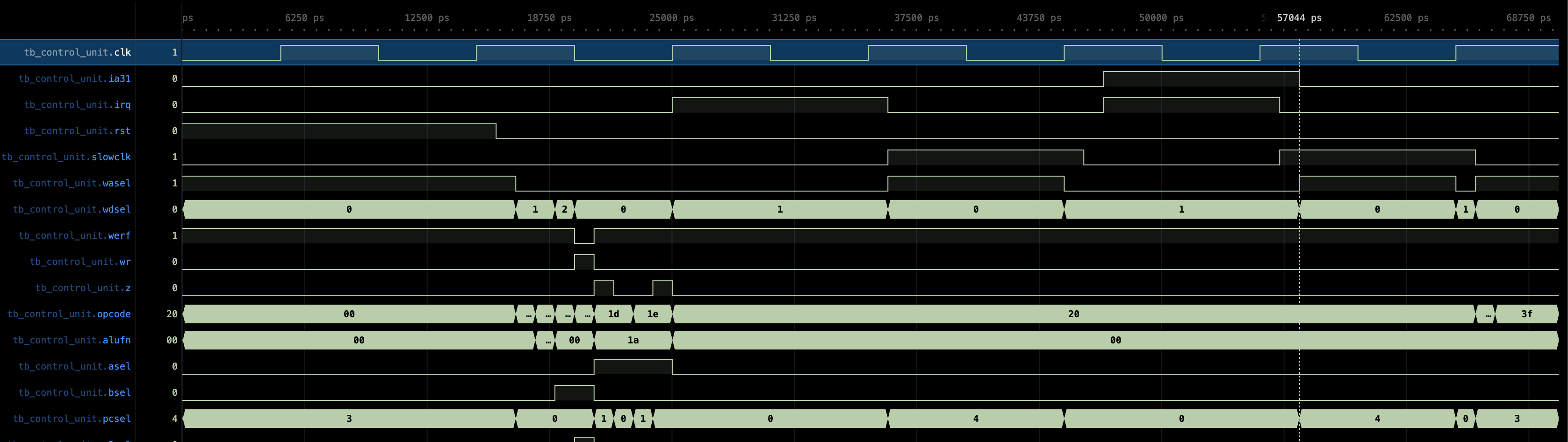
Note that the CU unit is mostly combinational, except the irq sampler.
Part D: Assemble Completed Beta
Task 12
The complete schematic of the Beta is as follows (you might want to open this image in another tab and zoom in):
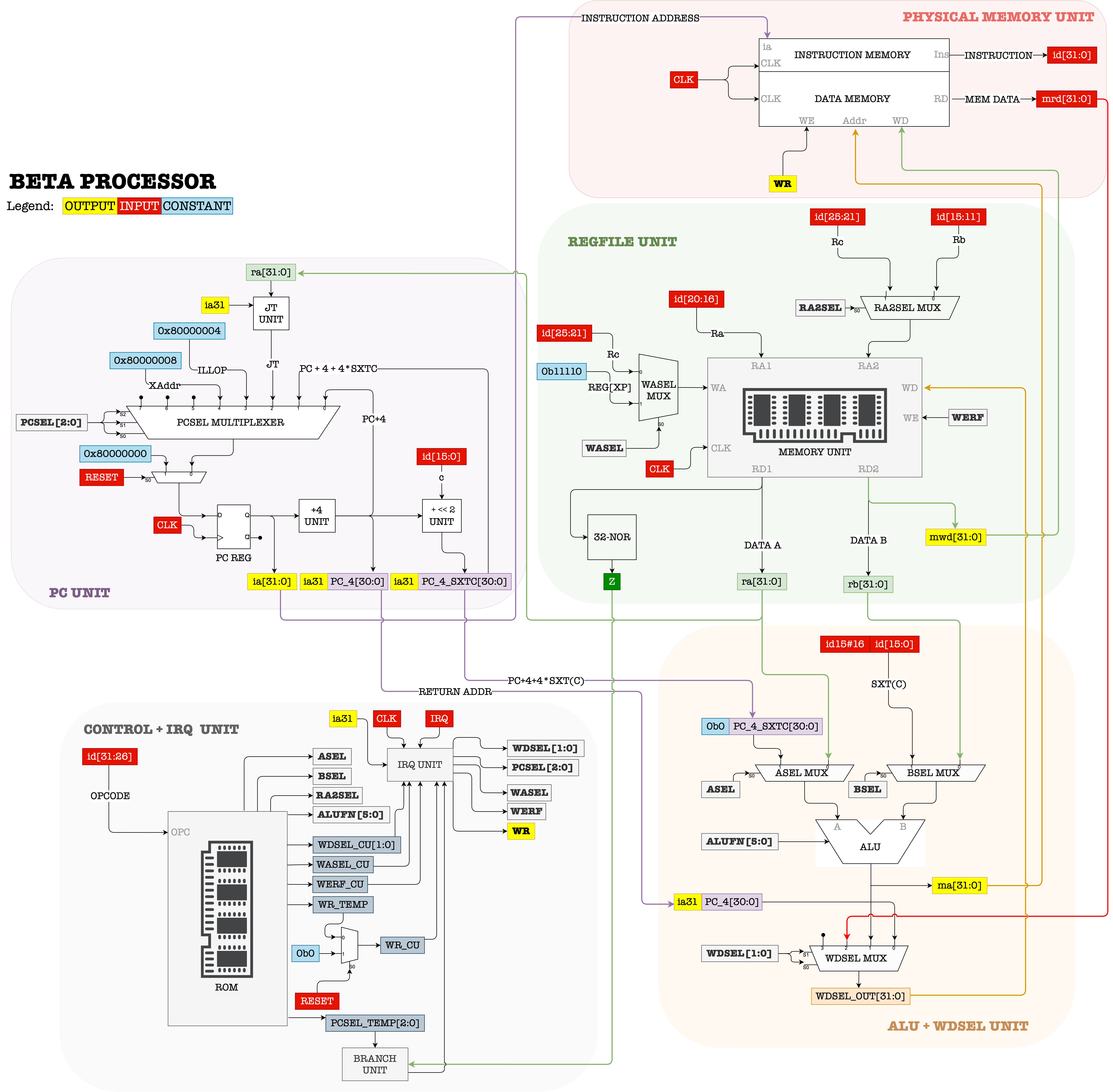
This is a suggested interface:
module beta_cpu (
    input         clk,
    input         slowclk,
    input         rst,
    input         irq,
    input  [31:0] instruction,
    input  [31:0] mem_data_input,
    output [31:0] ia,
    output [31:0] mem_data_address,
    output [31:0] mem_data_output,
    output        wr,
    output [15:0] debug_0,
    output [15:0] debug_1,
    output [15:0] debug_2,
    output [15:0] debug_3
);
ALU + WDSEL Unit
This unit is fairly straightforward to implement.
ALU+WDSEL Unit Schematic
Here is the suggested ALU + WDSEL Unit schematic that we implemented:
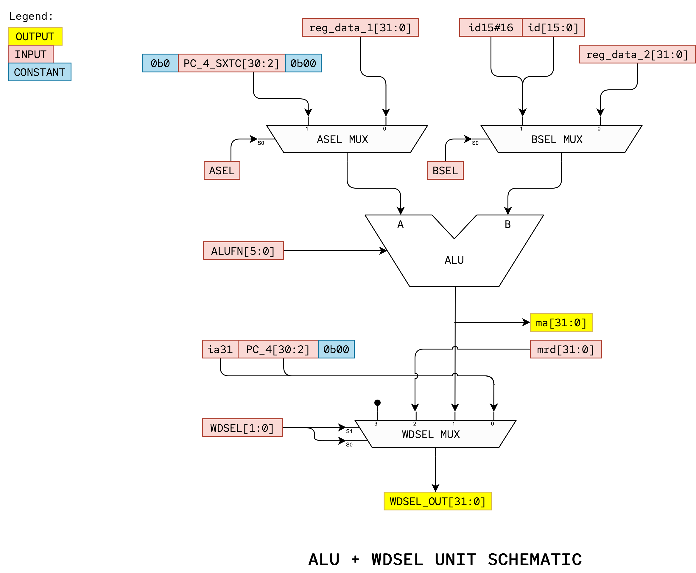
ASEL and BSEL Mux
The low-order 16 bits of the instruction need to be sign-extended to 32 bits as an input to the BSEL MUX. You have done sign extension before in Lab 2. Consult Lab 2 handout if you have forgotten how to do so.
Also, Bit 31 of the branch-offset input to the ASEL MUX should be set to 0. This means that the supervisor bit is ignored when doing address arithmetic for the LDR instruction.
WDSEL Mux
Bit 31 of the PC+4 input to the WDSEL MUX should connect to the highest bit of the PC Reg output, ia31, saving the current value of the supervisor whenever the value of the PC is saved by a branch instruction or trap. This is already handled in the PC unit. You don’t need to do anything else here.
Connect Debug Signals
It is really hard to debug your FPGA and it takes a long time to compile your Verilog code. As such, it always helps to create additional debug output so that we can “inspect” the content of each crucial component in the Beta CPU during each instruction execution when confirming the process in hardware.
Therefore, we proposed the 4 debug ports which you can connect to allow the top module to “view” the following:
  assign debug_0          = pcsel_out[15:0];
  assign debug_1          = asel_out[15:0];
  assign debug_2          = bsel_out[15:0];
  assign debug_3          = wdsel_out[15:0];
Testbench
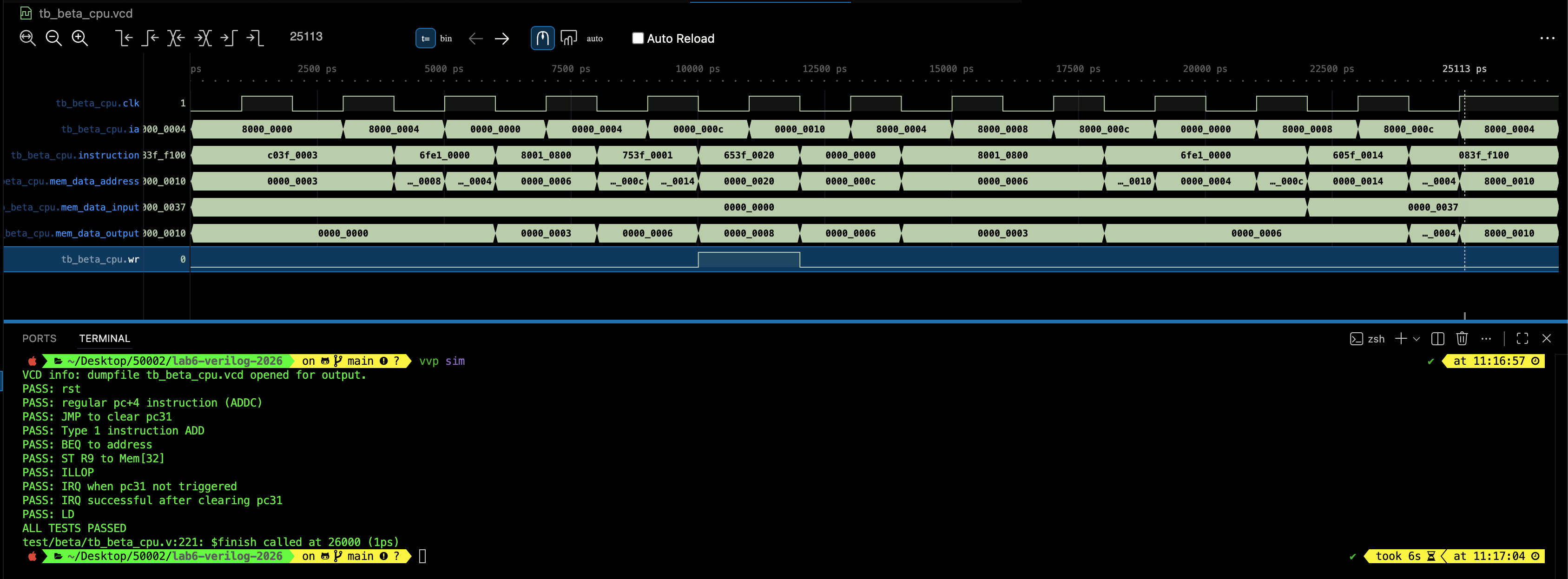
`timescale 1ns / 1ps

module tb_beta_cpu;

  // -----------------------------
  // DUT inputs
  // -----------------------------
  reg         clk;
  reg         slowclk;
  reg         rst;
  reg         irq;
  reg  [31:0] instruction;
  reg  [31:0] mem_data_input;

  // -----------------------------
  // DUT outputs
  // -----------------------------
  wire [31:0] ia;
  wire [31:0] mem_data_address;
  wire [31:0] mem_data_output;
  wire        wr;

  wire [15:0] debug_0;
  wire [15:0] debug_1;
  wire [15:0] debug_2;
  wire [15:0] debug_3;

  // -----------------------------
  // Instantiate DUT
  // -----------------------------
  beta_cpu dut (
      .clk             (clk),
      .slowclk         (slowclk),
      .rst             (rst),
      .irq             (irq),
      .instruction     (instruction),
      .mem_data_input  (mem_data_input),
      .ia              (ia),
      .mem_data_address(mem_data_address),
      .mem_data_output (mem_data_output),
      .wr              (wr),
      .debug_0         (debug_0),
      .debug_1         (debug_1),
      .debug_2         (debug_2),
      .debug_3         (debug_3)
  );

  // -----------------------------
  // Helpers (Verilog-2005 friendly)
  // -----------------------------
  task tick_clock;
    begin
      clk = 1'b0;
      #1;
      clk = 1'b1;
      #1;
    end
  endtask

  task assert_eq32;
    input [31:0] got;
    input [31:0] exp;
    input [1023:0] msg;
    begin
      if (got !== exp) begin
        $display("ASSERT FAIL: %s | got=0x%08h exp=0x%08h (t=%0t)", msg, got, exp, $time);
        $finish;
      end
    end
  endtask

  task assert_eq1;
    input got;
    input exp;
    input [1023:0] msg;
    begin
      if (got !== exp) begin
        $display("ASSERT FAIL: %s | got=%b exp=%b (t=%0t)", msg, got, exp, $time);
        $finish;
      end
    end
  endtask


  // --------------------------------------------------------------------------
  // Wave dump
  // --------------------------------------------------------------------------
  initial begin
    $dumpfile("tb_beta_cpu.vcd");
    $dumpvars(0, tb_beta_cpu);
  end

  // -----------------------------
  // Test sequence
  // -----------------------------
  initial begin
    // init
    clk = 1'b0;
    irq = 1'b0;
    slowclk = 1'b1;
    rst = 1'b0;
    instruction = 32'h00000000;
    mem_data_input = 32'h00000000;

    // -------------------------
    // test rst
    // -------------------------
    rst = 1'b1;
    instruction = 32'hC03F0003;  // ADDC(R31, 3, R1)
    mem_data_input = 32'h00000000;
    tick_clock();

    assert_eq32(ia, 32'h80000000, "rst: ia should be 0x80000000");
    assert_eq1(wr, 1'b0, "rst: wr should be 0");
    $display("PASS: rst");

    // -------------------------
    // regular pc+4 after rst
    // -------------------------
    rst = 1'b0;
    instruction = 32'hC03F0003;  // ADDC(R31, 3, R1)
    tick_clock();

    assert_eq32(ia, 32'h80000004, "ADDC: ia should be pc+4");
    assert_eq32(mem_data_address, 32'h00000003, "ADDC: alu_out (mem_data_address) should be 3");
    $display("PASS: regular pc+4 instruction (ADDC)");

    // -------------------------
    // JMP to clear the pc31 bit
    // at this point, R1 = 3
    // -------------------------
    instruction = 32'h6FE10000;  // JMP(R1)
    tick_clock();

    assert_eq32(ia, 32'h00000000, "JMP: ia should be 0x00000000 (LSBs protected)");
    $display("PASS: JMP to clear pc31");

    // -------------------------
    // Type 1 instruction
    // at this point, R1 = 3
    // -------------------------
    instruction = 32'h80010800;  // ADD(R1, R1, R0)
    tick_clock();

    assert_eq32(ia, 32'h00000004, "ADD: ia should be pc+4");
    assert_eq32(mem_data_address, 32'h00000006, "ADD: alu_out should be 6 (3+3)");
    $display("PASS: Type 1 instruction ADD");

    // -------------------------
    // Branch
    // -------------------------
    instruction = 32'h753F0001;  // BEQ(R31, to pc 12, R9)
    tick_clock();

    assert_eq32(ia, 32'd12, "BEQ: ia should branch to 12");
    $display("PASS: BEQ to address");

    // -------------------------
    // Store to address 32 in Memory
    // at this point, R9 = 8
    // -------------------------
    instruction = 32'h653F0020;  // ST(R9, 32, R31)
    tick_clock();

    assert_eq32(ia, 32'd16, "ST: ia should be pc+4 (16)");
    assert_eq32(mem_data_address, 32'd32, "ST: mem_data_address should be 32");
    assert_eq32(mem_data_output, 32'd8, "ST: mem_data_output should be 8");
    $display("PASS: ST R9 to Mem[32]");

    // -------------------------
    // test ILLOP
    // -------------------------
    instruction = 32'h00000000;
    tick_clock();

    assert_eq32(ia, 32'h80000004, "ILLOP: ia should go to 0x80000004");
    $display("PASS: ILLOP");

    // -------------------------
    // test IRQ (fail)
    // -------------------------
    instruction = 32'h80010800;  // ADD(R1, R1, R0)
    tick_clock();

    irq = 1'b1;
    tick_clock();

    assert_eq32(ia, 32'h8000000C, "IRQ fail-case: ia should be 0x8000000C");
    $display("PASS: IRQ when pc31 not triggered");

    // -------------------------
    // test IRQ (success)
    // at this point, R1 = 3
    // -------------------------
    instruction = 32'h6FE10000;  // JMP(R1)
    tick_clock();  // clears ia31 bit

    irq = 1'b1;
    tick_clock();

    assert_eq32(ia, 32'h80000008, "IRQ success-case: ia should be 0x80000008");
    $display("PASS: IRQ successful after clearing pc31");

    // -------------------------
    // test LD
    // -------------------------
    instruction = 32'h605F0014;  // LD(R31, Mem[20], R2)
    mem_data_input = 32'd55;  // assume Mem[20] = 55
    tick_clock();

    // Dummy instruction to route R2 somewhere observable
    instruction = 32'h83FF1000;
    tick_clock();

    assert_eq32(ia, 32'h80000010, "LD: ia should be 0x80000010 after dummy step");
    assert_eq32(mem_data_address, 32'd55,
                "LD: mem_data_address should reflect 55 in this test expectation");
    $display("PASS: LD");

    $display("ALL TESTS PASSED");
    $finish;
  end

endmodule
When successfully run, it will print the following message and produce the following waveform:
The Motherboard
Our final job is to now connect the Memory Unit and the Beta CPU together, and run the series of instructions. We need to first load the instructions into the instruction memory, and then let the Beta CPU run as long as slowclk is high.
MMIO
We can also support a little bit of IO, in particular, MMIO style (memory-mapped IO) where the motherboard decides whether the Beta CPU reads from an input reg or Memory Unit, and write to an output reg or Memory Unit based on the address given at mem_data_address port.
In particular:
0x000F000: output reg (write)0x000E000: input reg (read)
Implementation
Here’s a simple implementation of the motherboard, complete with MMIO.
module motherboard #(
    parameter integer WORDS = 64
) (
    input wire clk,
    input wire rst,
    input wire irq,
    input wire slowclk, // pulse of slow clock

    // input device reg
    input wire [31:0] in_reg,

    // output device reg
    output wire [31:0] out_reg,

    output wire [31:0] id_out,
    output wire [31:0] ia_out,
    output wire [31:0] ea_out,   // EA
    output wire [31:0] mrd_out,  // mem[EA]
    output wire [31:0] mwd_out,

    output wire [15:0] pcsel_out,
    output wire [15:0] asel_out,
    output wire [15:0] bsel_out,
    output wire [15:0] wdsel_out
);

  // cpu wires
  wire [31:0] id;
  wire [31:0] mem_data_input = is_mmio_in ? mmio_in_q : mrd;
  wire [31:0] ia;
  wire [31:0] mem_data_address;
  wire [31:0] mem_data_output;
  wire        wr;
  wire [15:0] debug_0;
  wire [15:0] debug_1;
  wire [15:0] debug_2;
  wire [15:0] debug_3;

  // memory unit wires
  wire        we = wr & ~is_mmio_out;
  wire [31:0] mrd;

  // mmio decode
  wire        is_mmio_out = (mem_data_address == 32'h000F0000);
  wire        is_mmio_in = (mem_data_address == 32'h000E0000);

  // mmio wires
  wire [31:0] mmio_out_q;
  wire [31:0] mmio_in_q;

  wire        mmio_out_we = wr & is_mmio_out;

  // mmio regs
  // output device
  register #(
      .W(32),
      .RESET_VALUE(0)
  ) u_mmio_out (
      .clk(clk),
      .rst(rst),
      .en (mmio_out_we),
      .d  (mem_data_output),
      .q  (mmio_out_q)
  );
  // input device
  // written to only when interrupt is high
  // store on interrupt
  // can only be read one cycle later
  register #(
      .W(32),
      .RESET_VALUE(0)
  ) u_mmio_in (
      .clk(clk),
      .rst(rst),
      .en (irq),
      .d  (in_reg),
      .q  (mmio_in_q)
  );


  beta_cpu u_beta_cpu (
      .clk(clk),
      .slowclk(slowclk),
      .rst(rst),
      .irq(irq),
      .id(id),
      .mem_data_input(mem_data_input),
      .ia(ia),
      .mem_data_address(mem_data_address),
      .mem_data_output(mem_data_output),
      .wr(wr),
      .debug_0(debug_0),
      .debug_1(debug_1),
      .debug_2(debug_2),
      .debug_3(debug_3)
  );


  reg i_we;

  memory_unit #(
      .WORDS(WORDS)
  ) memory_unit (
      .clk(clk),
      .raddr(mem_data_address),
      .waddr(mem_data_address),
      .wd(mem_data_output),
      .we(we),
      .mrd(mrd),
      .ia(ia),
      .id(id)
  );


  // output signals
  assign out_reg = mmio_out_q;

  assign id_out = id;
  assign ia_out = ia;
  assign ea_out = mem_data_address;  // EA
  assign mrd_out = mrd;  // mem[EA]
  assign mwd_out = mem_data_output;

  assign pcsel_out = debug_0;
  assign asel_out = debug_1;
  assign bsel_out = debug_2;
  assign wdsel_out = debug_3;

endmodule
clk Requirements
write requires two clock cycles, so any ST cannot be immediately followed by LD in the next clk cycle. The easiest way to do this is to ensure that slowclk signal is at least four times slower than original clk cycle, to allow time for the memory unit to latch and store, should we have instructions of LD immediately after ST.
This is also useful if BRAM firmware is used, where instruction read is no longer combinational (it becomes sequential with 1 clk cycle latency). See this section.
Testbench
This simple tb generates the waveform based on the current instructions given:
`timescale 1ns / 1ps

module tb_motherboard;

  localparam integer WORDS = 64;

  // ------------------------------------------------------------
  // DUT inputs
  // ------------------------------------------------------------
  reg         clk;
  reg         rst;
  reg         irq;
  reg         slowclk;
  reg  [31:0] in_reg;

  // ------------------------------------------------------------
  // DUT outputs
  // ------------------------------------------------------------
  wire [31:0] out_reg;

  wire [31:0] id_out;
  wire [31:0] ia_out;
  wire [31:0] ea_out;
  wire [31:0] mrd_out;
  wire [31:0] mwd_out;

  wire [15:0] pcsel_out;
  wire [15:0] asel_out;
  wire [15:0] bsel_out;
  wire [15:0] wdsel_out;

  // ------------------------------------------------------------
  // Instantiate DUT
  // ------------------------------------------------------------
  motherboard #(
      .WORDS(WORDS)
  ) dut (
      .clk(clk),
      .rst(rst),
      .irq(irq),
      .slowclk(slowclk),

      .in_reg (in_reg),
      .out_reg(out_reg),

      .id_out (id_out),
      .ia_out (ia_out),
      .ea_out (ea_out),
      .mrd_out(mrd_out),
      .mwd_out(mwd_out),

      .pcsel_out(pcsel_out),
      .asel_out (asel_out),
      .bsel_out (bsel_out),
      .wdsel_out(wdsel_out)
  );

  // ------------------------------------------------------------
  // Clock: 100 MHz
  // ------------------------------------------------------------
  initial clk = 1'b0;
  always #5 clk = ~clk;

  // ------------------------------------------------------------
  // slowclk: 1-cycle pulse every 4 clk cycles
  // e.g. high on cycles 4,8,12,... for one clk each time
  // ------------------------------------------------------------
  reg [1:0] scnt;
  always @(posedge clk) begin
    if (rst) begin
      scnt    <= 2'd0;
      slowclk <= 1'b0;
    end else begin
      scnt <= scnt + 2'd1;
      slowclk <= (scnt == 2'd3);  // 1-cycle pulse
    end
  end

  // ------------------------------------------------------------
  // Wave dump
  // ------------------------------------------------------------
  initial begin
    $dumpfile("tb_motherboard.vcd");
    $dumpvars(0, tb_motherboard);
  end

  // ------------------------------------------------------------
  // Stimulus
  // ------------------------------------------------------------
  initial begin
    // init
    rst    = 1'b1;
    irq    = 1'b0;
    in_reg = 32'h0000_0000;

    // hold reset a few cycles
    repeat (4) @(posedge clk);
    rst = 1'b0;

    // let CPU "manual advance" via slowclk pulses
    repeat (20) @(posedge clk);

    // poke input device and interrupt to latch mmio_in_q
    in_reg = 32'hDEAD_BEEF;
    irq    = 1'b1;
    @(posedge clk);
    irq = 1'b0;

    repeat (20) @(posedge clk);

    in_reg = 32'h1234_5678;
    irq    = 1'b1;
    @(posedge clk);
    irq = 1'b0;

    // run a bit more
    repeat (60) @(posedge clk);

    $finish;
  end

endmodule
You should obtain the following waveform, where ia is looping between the 5 instructions in address 0x80000000 to 0x80000010.
What to check (manually):
iamatchesidas per what you specified infirmwareiaadvances onslowclkirqdoesnt interrupt whenia31is1BNE/BEQis computed successfullyLD/STworks without issue
Using BRAM for firmware
The firmware offered above still uses combinational logic, and it can be quite expensive depending on the amount of instructions you want to store.
You can use the BRAM for this, but to get BRAM inference you need a synchronous-read memory array (registered output). Here’s one implementation. It keeps the same logical interface, just that we use clk here:
`timescale 1ns / 1ps
`define FW_HEX_FILE "data/firmware.mem"

module firmware_rom_bram #(
    parameter integer WORDS = 128
) (
    input  wire        clk,
    input  wire [31:0] ia,        // byte address
    output reg  [31:0] id,
    output wire [ 7:0] num_instr
);

  // Verilog-2005 clog2
  function integer clog2;
    input integer value;
    integer i;
    begin
      value = value - 1;
      for (i = 0; value > 0; i = i + 1) value = value >> 1;
      clog2 = i;
    end
  endfunction

  localparam integer AW = clog2(WORDS);

  // ROM storage
  reg [31:0] rom[0:WORDS-1];

  assign num_instr = 8'd5;

  wire [AW-1:0] ia_word;
  assign ia_word = ia[AW+1:2];

  initial begin
    // loads word 0 from line 0, word 1 from line 1, etc.
    $readmemh(`FW_HEX_FILE, rom);
  end

  always @(posedge clk) begin
    id <= rom[ia_word];
  end

endmodule
Then you instantiate this in memory_unit.v as:
firmware_rom #(.WORDS(128), .INIT_HEX("firmware.mem")) u_firmware_rom (
  .clk(clk),
  .ia(ia),
  .id(id),
  .num_instr(num_instr)
);
For the instruction data, store this inside data/firmware.hex. Note that the first line is the code fed to address 0.
C03F0003
90410800
643F0020
607F0020
7BE3FFFB
Adding memory file in Vivado
Choose the file type of Memory File in Vivado when adding Design Sources.
If you name your file properly, e.g: firmware.mem, Vivado is also able to find that file as you import. You can simply just define the hex file as-is in the header of firmware_bram.v. Vivado will find the file and figure out the pathing automatically.
slowclk Requirement
Since instruction read takes 1 clk cycle, then slowclk must fire once at most every two clk cycles. Here we fire slowclk every 4 clk cycles and obtain the following waveform. You can see clearly that id is produced synchronously with the clk, which means we have 1 clk cycle latency from the moment we produce ia.
Connecting it with hardware
The one thing left to do is to connect the signals into buttons and leds defined in alchitry_top. You can use the suggested alchitry_top_verilog below which flattened the io_dip and io_leds. io_button[0] is used as “next” (slowclk) button, and io_button[1] is used as interrupt button, to capture the status of the 24 dips as MMIO.
UI
We shall use the same UI interface as defined in the official lab.
io_dip[0] can be changed to “view” various states presented at io_led[1] and io_led[0] (16 bits of values at once). Simply set it to represent the values below, e.g: 0x3 means that io_dip[0] is set to 00000011 (turn the rightmost two switches on). Here is the exhaustive list:
0x0: MSB 16 bits of current instruction (id[31:16])0x1: LSB 16 bits of current instruction (id[15:0])0x2: LSB 16 bits of instruction address (ia[15:0])0x3: LSB 16 bits of EA (this is also ALU output) (ma[15:0])0x4: MSB 16 bits of EA (this is also ALU output) (ma[31:16])0x5: LSB 16 bits of Mem[EA] (mrd[15:0])0x6: MSB 16 bits of Mem[EA] (mrd[31:16])0x7: LSB 16 bits of RD2 (mwd[15:0])0x8: MSB 16 bits of RD2 (mwd[31:16])0x9: LSB 16 bits of pcsel_out0xA: LSB 16 bits of asel_out0xB: LSB 16 bits of bsel_out0xC: LSB 16 bits of wdsel_out0xD: MSB 16 bits of instruction address. Useful to see PC31 (kernel/user mode) (ia[31:16])0xE: LSB 16 bits of beta input buffer. This is a dff that’s hardwired to reflect Mem[0x10]0xF: LSB 16 bits of beta output buffer. This is a dff that’s hardwired to reflect Mem[0xC]
Suggested Verilog top file
The Verilog Top file processes all I/O (passing it through conditioners and edge detectors) where necessary and connects it to the motherboard:
`timescale 1ns / 1ps

module alchitry_top_verilog (
    input            clk,
    input            rst_n,
    output reg [7:0] led,
    input            usb_rx,
    output reg       usb_tx,

    output reg [23:0] io_led_flat,

    output reg [7:0] io_segment,
    output reg [3:0] io_select,
    input      [4:0] io_button,

    input [23:0] io_dip_flat
);

  // ------------------------------------------------------------
  // Basic always-on IO defaults
  // ------------------------------------------------------------

  always @* begin
    usb_tx     = usb_rx;
    io_segment = 8'hFF;
    io_select  = 4'hF;
  end

  // ------------------------------------------------------------
  // DIP unpack
  // ------------------------------------------------------------
  wire [7:0] io_dip0 = io_dip_flat[7:0];  // io_dip[0]
  wire [7:0] io_dip1 = io_dip_flat[15:8];  // io_dip[1]
  wire [7:0] io_dip2 = io_dip_flat[23:16];  // io_dip[2]

  wire [3:0] view_sel = io_dip0[3:0];

  // ------------------------------------------------------------
  // Slowclk from button 0: conditioner + rising-edge detector
  // ------------------------------------------------------------
  wire       btn_raw = io_button[0];
  wire       btn_cond;

  button_conditioner #(
      .CLK_FREQ (27'h5f5e100),
      .MIN_DELAY(5'h14),
      .NUM_SYNC (2'h2)
  ) u_bc (
      .clk(clk),
      .in (btn_raw),
      .out(btn_cond)
  );

  wire slowclk_pulse;

  edge_detector #(
      .RISE(1),
      .FALL(0)
  ) u_ed_1 (
      .clk(clk),
      .in (btn_cond),
      .out(slowclk_pulse)
  );
  // ------------------------------------------------------------
  // IRQ from button 1: conditioner + rising-edge detector
  // ------------------------------------------------------------
  wire btn_raw_1 = io_button[1];
  wire btn_cond_1;

  button_conditioner #(
      .CLK_FREQ (27'h5f5e100),
      .MIN_DELAY(5'h14),
      .NUM_SYNC (2'h2)
  ) u_bc_1 (
      .clk(clk),
      .in (btn_raw_1),
      .out(btn_cond_1)
  );

  wire btn_1_pulse;

  edge_detector #(
      .RISE(1),
      .FALL(0)
  ) u_ed_2 (
      .clk(clk),
      .in (btn_cond_1),
      .out(btn_1_pulse)
  );

  // ------------------------------------------------------------
  // reset conditioner
  // ------------------------------------------------------------
  wire rst_cond;
  wire rst = ~rst_cond;

  reset_conditioner u_reset_conditioner (
      .clk(clk),
      .in (rst_n),
      .out(rst_cond)
  );
  // ------------------------------------------------------------
  // Motherboard instance
  // ------------------------------------------------------------
  wire [31:0] out_reg_w;

  wire [31:0] id_out;
  wire [31:0] ia_out;
  wire [31:0] ea_out;
  wire [31:0] mrd_out;
  wire [31:0] mwd_out;

  wire [15:0] pcsel_out;
  wire [15:0] asel_out;
  wire [15:0] bsel_out;
  wire [15:0] wdsel_out;

  // Choose what drives in_reg:
  // Option: pack dips into 32-bit so you can "type" values from switches.
  wire [31:0] in_reg_w = {8'h00, io_dip2, io_dip1, io_dip0};

  // irq source: you can map a button (e.g. io_button[1]) or dip bit.
  wire irq_w = btn_1_pulse;

  motherboard #(
      .WORDS(64)
  ) u_mb (
      .clk(clk),
      .rst(rst),
      .irq(irq_w),
      .slowclk(slowclk_pulse),

      .in_reg (in_reg_w),
      .out_reg(out_reg_w),

      .id_out (id_out),
      .ia_out (ia_out),
      .ea_out (ea_out),
      .mrd_out(mrd_out),
      .mwd_out(mwd_out),

      .pcsel_out(pcsel_out),
      .asel_out (asel_out),
      .bsel_out (bsel_out),
      .wdsel_out(wdsel_out)
  );

  // ------------------------------------------------------------
  // Viewer mux: select 16-bit value to show on io_led[1:0]
  // io_led_flat[15:0] = {io_led[1], io_led[0]}
  // ------------------------------------------------------------
  reg [15:0] view16;

  always @* begin
    case (view_sel)
      4'h0: view16 = id_out[31:16];
      4'h1: view16 = id_out[15:0];
      4'h2: view16 = ia_out[15:0];
      4'h3: view16 = ea_out[15:0];
      4'h4: view16 = ea_out[31:16];
      4'h5: view16 = mrd_out[15:0];
      4'h6: view16 = mrd_out[31:16];
      4'h7: view16 = mwd_out[15:0];
      4'h8: view16 = mwd_out[31:16];
      4'h9: view16 = pcsel_out[15:0];
      4'hA: view16 = asel_out[15:0];
      4'hB: view16 = bsel_out[15:0];
      4'hC: view16 = wdsel_out[15:0];
      4'hD: view16 = ia_out[31:16];
      4'hE: view16 = in_reg_w[15:0];     // your "beta input buffer" view
      4'hF: view16 = out_reg_w[15:0];    // your "beta output buffer" view
      default: view16 = 16'h0000;
    endcase
  end

  // Drive LEDs
  always @* begin
    // Put view16 on LED banks 0 and 1
    io_led_flat[7:0] = view16[7:0];
    io_led_flat[15:8] = view16[15:8];

    // Use LED bank 2 for something useful (optional)
    io_led_flat[23:16] = {view_sel, btn_cond_1, btn_cond, irq_w, slowclk_pulse};

    // Also drive the onboard 8 LEDs with out_reg low byte (optional)
    led = out_reg_w[7:0];
  end

endmodule
The module above uses button_conditioner and edge_detector. See appendix.
Combine with default alchitry_top.sv
You can then wrap the above with alchitry_top.sv available in the starter code. If you’re unsure how to use this, read this guide.
module alchitry_top(
    input  logic clk,
    input  logic rst_n,
    output logic [7:0] led,
    input  logic usb_rx,
    output logic usb_tx,
    output logic [2:0][7:0] io_led,
    output logic [7:0] io_segment,
    output logic [3:0] io_select,
    input  logic [4:0] io_button,
    input  logic [2:0][7:0] io_dip
);

  // pack SV arrays into flat vectors for the Verilog-2005 module
  wire [23:0] io_dip_flat = { io_dip[2], io_dip[1], io_dip[0] };
  wire [23:0] io_led_flat;

  // unpack flat vector back into SV array
  assign { io_led[2], io_led[1], io_led[0] } = io_led_flat;

  alchitry_top_verilog u_core (
    .clk(clk),
    .rst_n(rst_n),
    .led(led),
    .usb_rx(usb_rx),
    .usb_tx(usb_tx),
    .io_led_flat(io_led_flat),
    .io_segment(io_segment),
    .io_select(io_select),
    .io_button(io_button),
    .io_dip_flat(io_dip_flat)
  );

endmodule
If you don’t use Vivado IDE, you can also use alchitry_top.luc and Alchitry Labs IDE as per normal after importing all necessary verilog files and connect the signals together.
Compile and Run
Congratulations! 🎉
You have made a working Beta CPU. Please take your time to understand how each component works. You shall now compile, run the program and then vary io_dip[0] switches to inspect each state.
What next?
You can try new types of instructions that utilises the MMIO.
Appendix
Unified Memory Model
In practice, the instruction memory and data memory are only logically segregated. Architecturally, the CPU treats them as separate spaces because they serve different purposes, but physically they can reside in the same RAM device.
What the CPU actually requires in a single cycle is:
- one instruction fetch (read),
- one data load (read), and
- optionally one data store (write).
This access pattern corresponds to a 2-read, 1-write (2R1W) memory.
Physical Realisation on FPGA
Most FPGA block RAMs natively support at most two ports. A true 2R1W memory is therefore not directly available as a single primitive. In practice, FPGA designs implement this behaviour using one of the following techniques:
-
Separate instruction and data memories (what we do): Instruction memory and data memory are instantiated as two independent RAM blocks. This is simple to reason about and is commonly used in teaching designs.
-
Replicated memory: Two identical copies of the same memory are created. This technique provides the illusion of a single unified memory with two independent read ports and one write port.
- one copy services the instruction read port, and
- the other copy services the data read port.
- Any write operation updates both copies, ensuring that the two read ports always observe consistent memory contents.
Below is a sample implementation for method (2):
// Unified RAM: 2 read ports (ia + raddr) and 1 write port (waddr)
// Byte-addressed inputs, word-aligned internally (addr >> 2)
//
// Implementation: replicated RAM for the two read ports.
// Any write updates BOTH copies so both reads see the same memory contents.
module memory_unit_2r1w #(
    parameter integer WORDS = 16
)(
    input  wire clk,

    // instruction fetch (byte addressing expected)
    input  wire [$clog2(WORDS)+2-1:0] ia,
    output reg  [31:0]                id,

    // data read (byte addressing expected)
    input  wire [$clog2(WORDS)+2-1:0] raddr,
    output reg  [31:0]                mrd,

    // data write (byte addressing expected)
    input  wire [$clog2(WORDS)+2-1:0] waddr,
    input  wire [31:0]                wd,
    input  wire                       we
);

  localparam integer AW = $clog2(WORDS);

  wire [AW-1:0] ia_word = ia[AW+1:2];
  wire [AW-1:0] ra_word = raddr[AW+1:2];
  wire [AW-1:0] wa_word = waddr[AW+1:2];

  // Two identical copies to get two independent synchronous read ports
  // Tells synthesis tool to implement this array as block RAM (BRAM) instead of flip-flops (LUT RAM)
  (* ram_style = "block" *) reg [31:0] mem_i [0:WORDS-1]; // for instruction read
  (* ram_style = "block" *) reg [31:0] mem_d [0:WORDS-1]; // for data read

  integer k;
  initial begin
    // Optional: init to 0 for simulation friendliness
    for (k = 0; k < WORDS; k = k + 1) begin
      mem_i[k] = 32'h0;
      mem_d[k] = 32'h0;
    end
  end

  always @(posedge clk) begin
    // synchronous reads (1-cycle latency)
    id  <= mem_i[ia_word];
    mrd <= mem_d[ra_word];

    // write updates BOTH copies
    if (we) begin
      mem_i[wa_word] <= wd;
      mem_d[wa_word] <= wd;
    end
  end

endmodule
Note that if you use this construct, then the addresses used in LD, ST and LDR instruction would differ from when you use the separated instruction-data construct.
Timing Semantics
All memory accesses are synchronous:
- Read data is returned in the next clock cycle.
- Write data is committed at the end of the current cycle if the write enable is asserted.
As a result:
- Instruction fetch and data load addresses are presented in cycle N.
- The corresponding values become visible in cycle N+1.
Addressing Convention (Byte Address In, Word-Aligned)
The memory unit accepts byte addresses at its interface, but stores data internally as 32-bit words. Therefore, the memory is word-aligned:
- The lowest two bits of every address (
addr[1:0]) are ignored. - The internal word index is effectively
addr >> 2.
This is implemented by slicing the address as follows:
addr_word = addr[$clog2(WORDS)+2-1 : 2];
Consequences:
- Addresses that differ only in the lowest two bits map to the same word.
- Unaligned byte or halfword accesses are not supported and are implicitly forced to the nearest aligned word.
A strictly byte-addressable memory could be implemented by storing 8-bit entries and assembling 32-bit words in logic, but this would significantly complicate the design. For the Beta CPU, a word-aligned memory provides a cleaner and more instructive model.
simple_ram.v
/******************************************************************************

   The MIT License (MIT)

   Copyright (c) 2026 Alchitry

   Permission is hereby granted, free of charge, to any person obtaining a copy
   of this software and associated documentation files (the "Software"), to deal
   in the Software without restriction, including without limitation the rights
   to use, copy, modify, merge, publish, distribute, sublicense, and/or sell
   copies of the Software, and to permit persons to whom the Software is
   furnished to do so, subject to the following conditions:

   The above copyright notice and this permission notice shall be included in
   all copies or substantial portions of the Software.

   THE SOFTWARE IS PROVIDED "AS IS", WITHOUT WARRANTY OF ANY KIND, EXPRESS OR
   IMPLIED, INCLUDING BUT NOT LIMITED TO THE WARRANTIES OF MERCHANTABILITY,
   FITNESS FOR A PARTICULAR PURPOSE AND NONINFRINGEMENT. IN NO EVENT SHALL THE
   AUTHORS OR COPYRIGHT HOLDERS BE LIABLE FOR ANY CLAIM, DAMAGES OR OTHER
   LIABILITY, WHETHER IN AN ACTION OF CONTRACT, TORT OR OTHERWISE, ARISING FROM,
   OUT OF OR IN CONNECTION WITH THE SOFTWARE OR THE USE OR OTHER DEALINGS IN
   THE SOFTWARE.

   *****************************************************************************

   This module is a simple single port RAM. This RAM is implemented in such a
   way that the tools will recognize it as a RAM and implement large
   instances in block RAM instead of flip-flops.

   The parameter WIDTH is used to specify the word size. That is the size of
   each entry in the RAM.

   The parameter ENTRIES is used to specify how many entries are in the RAM.

   read_data outputs the value of the entry pointed to by address in the previous
   clock cycle. That means to read address 10, you would set address to be 10
   and wait one cycle for its value to show up. The RAM is always reading whatever
   address is. If you don't need to read, just ignore this value.

   To write, set write_enable to 1, write_data to the value to write,
   and address to the address you want to write.

   If you read and write the same address, the first clock cycle the address will
   be written, the second clock cycle the old value will be output on read_data,
   and on the third clock cycle the newly updated value will be output on
   read_data.
*/

module simple_ram #(
    parameter WIDTH = 1,                  // size of each entry
    parameter ENTRIES = 1                 // number of entries
  )(
    input clk,                            // clock
    input [$clog2(ENTRIES)-1:0] address,  // address to read or write
    output reg [WIDTH-1:0] read_data,     // data read
    input [WIDTH-1:0] write_data,         // data to write
    input write_enable                    // write enable (1 = write)
  );

  reg [WIDTH-1:0] ram [ENTRIES-1:0];      // memory array

  always @(posedge clk) begin
    read_data <= ram[address];            // read the entry

    if (write_enable)                     // if we need to write
      ram[address] <= write_data;         // update that value
  end

endmodule
simple_dual_port_ram.v
/******************************************************************************

   The MIT License (MIT)

   Copyright (c) 2026 Alchitry

   Permission is hereby granted, free of charge, to any person obtaining a copy
   of this software and associated documentation files (the "Software"), to deal
   in the Software without restriction, including without limitation the rights
   to use, copy, modify, merge, publish, distribute, sublicense, and/or sell
   copies of the Software, and to permit persons to whom the Software is
   furnished to do so, subject to the following conditions:

   The above copyright notice and this permission notice shall be included in
   all copies or substantial portions of the Software.

   THE SOFTWARE IS PROVIDED "AS IS", WITHOUT WARRANTY OF ANY KIND, EXPRESS OR
   IMPLIED, INCLUDING BUT NOT LIMITED TO THE WARRANTIES OF MERCHANTABILITY,
   FITNESS FOR A PARTICULAR PURPOSE AND NONINFRINGEMENT. IN NO EVENT SHALL THE
   AUTHORS OR COPYRIGHT HOLDERS BE LIABLE FOR ANY CLAIM, DAMAGES OR OTHER
   LIABILITY, WHETHER IN AN ACTION OF CONTRACT, TORT OR OTHERWISE, ARISING FROM,
   OUT OF OR IN CONNECTION WITH THE SOFTWARE OR THE USE OR OTHER DEALINGS IN
   THE SOFTWARE.

   *****************************************************************************

   This module is a simple dual port RAM. This RAM is implemented in such a
   way that Xilinx's tools will recognize it as a RAM and implement large
   instances in block RAM instead of flip-flops.

   The parameter WIDTH is used to specify the word size. That is the size of
   each entry in the RAM.

   The parameter ENTRIES is used to specify how many entries are in the RAM.

   read_data outputs the value of the entry pointed to by raddr in the previous
   clock cycle. That means to read address 10, you would set address to be 10
   and wait one cycle for its value to show up. The RAM is always reading whatever
   address is. If you don't need to read, just ignore this value.

   To write, set write_enable to 1, write_data to the value to write, and waddr to
   the address you want to write.

   You should avoid reading and writing to the same address simultaneously. The
   value read in this case is undefined.
*/
module simple_dual_port_ram #(
    parameter WIDTH = 8,                // size of each entry
    parameter ENTRIES = 8               // number of entries
  )(
    // write interface
    input wclk,                         // write clock
    input [$clog2(ENTRIES)-1:0] waddr,  // write address
    input [WIDTH-1:0] write_data,       // write data
    input write_enable,                 // write enable (1 = write)

    // read interface
    input rclk,                         // read clock
    input [$clog2(ENTRIES)-1:0] raddr,  // read address
    output reg [WIDTH-1:0] read_data    // read data
  );

  reg [WIDTH-1:0] mem [ENTRIES-1:0];    // memory array

  // write clock domain
  always @(posedge wclk) begin
    if (write_enable)                   // if write enable
      mem[waddr] <= write_data;         // write memory
  end

  // read clock domain
  always @(posedge rclk) begin
    read_data <= mem[raddr];            // read memory
  end

endmodule
Reset Conditioner
`timescale 1ns / 1ps

module reset_conditioner #(
    parameter integer STAGES = 4
) (
    input  wire clk,
    input  wire in,
    output reg  out
);

  reg [STAGES-1:0] stage_q;

  // Combinational out is MSB of the shift register
  always @* begin
    out = stage_q[STAGES-1];
  end

  // Async assert, sync deassert (shift zeros in)
  always @(posedge clk or posedge in) begin
    if (in) begin
      stage_q <= {STAGES{1'b1}};
    end else begin
      stage_q <= {stage_q[STAGES-2:0], 1'b0};
    end
  end

endmodule
Button Conditioner
`timescale 1ns / 1ps

module button_conditioner #(
    parameter integer CLK_FREQ  = 100000000,  // Hz
    parameter integer MIN_DELAY = 20,         // ms
    parameter integer NUM_SYNC  = 2
) (
    input  wire clk,
    input  wire in,
    output reg  out
);


  function integer clog2;
    input integer value;
    integer v;
    begin
      v = value - 1;
      clog2 = 0;
      while (v > 0) begin
        v = v >> 1;
        clog2 = clog2 + 1;
      end
      if (clog2 < 1) clog2 = 1;
    end
  endfunction

  // Target cycles for MIN_DELAY ms (rounded down). Ensure >= 1.
  localparam integer TARGET_CYCLES_RAW = (CLK_FREQ / 1000) * MIN_DELAY;
  localparam integer TARGET_CYCLES = (TARGET_CYCLES_RAW < 1) ? 1 : TARGET_CYCLES_RAW;

    `ifdef SIM
    // Fast debounce for sim: 4 cycles to reach all-ones if CTR_W=2
    localparam integer CTR_W = 2;
    `else
    localparam integer CTR_W = clog2(TARGET_CYCLES);
    `endif

  // -----------------------------
  // Synchronizer chain
  // -----------------------------
  reg [NUM_SYNC-1:0] sync_ff;
  integer k;

  always @(posedge clk) begin
    sync_ff[0] <= in;
    for (k = 1; k < NUM_SYNC; k = k + 1) begin
      sync_ff[k] <= sync_ff[k-1];
    end
  end

  wire in_sync = sync_ff[NUM_SYNC-1];

  // -----------------------------
  // Debounce counter
  // -----------------------------
  reg [CTR_W-1:0] ctr;

  always @(posedge clk) begin
    if (!in_sync) begin
      ctr <= {CTR_W{1'b0}};
    end else if (!(&ctr)) begin
      ctr <= ctr + { {(CTR_W - 1) {1'b0} }, 1'b1};
    end
    out <= &ctr;
  end

endmodule
Edge Detector
module edge_detector #(
    parameter RISE = 1'b1,
    parameter FALL = 1'b1
) (
    input  wire clk,
    input  wire in,
    output reg  out
);

  reg last_q;

  initial begin
    last_q = 1'b0;
  end

  always @* begin
    out = 1'b0;

    if (RISE) begin
      if (in == 1'b1 && last_q == 1'b0) out = 1'b1;
    end

    if (FALL) begin
      if (in == 1'b0 && last_q == 1'b1) out = 1'b1;
    end
  end

  always @(posedge clk) begin
    last_q <= in;
  end

endmodule