 50.002 CS
- Objectives
- Submission
- Starter Code
- Related Class Materials
- Sequential Logic
- One Clock to Rule Them All
dffin Lucid- Creating a Pipeline
- Button-controlled Sampling
- Testbench
- Checkoff
- Summary
- Appendix
50.002 Computation Structures
Information Systems Technology and Design
Singapore University of Technology and Design
Lab 3: Clocked Circuits
Objectives
By the end of this lab, you should be able to:
- Explain how a global clock and D flip-flops (
dffs) enforce time boundaries in a digital circuit. - Use Lucid
dffs to build registers (with and without enable) and reason about their behaviour over clock cycles. - Construct a registered RCA (ripple-carry adder) and describe why output registers are needed for stable, pipeline-friendly outputs.
- Distinguish between unregistered combinational behaviour and registered, periodic behaviour when observing signals on LEDs.
- Design a button-controlled sampling scheme that captures input values only when triggered.
- Implement an automated, self-checking testbench for a registered adder using:
- constant test vectors,
- a systematic way to step through them over simulation time,
- and $assert checks against expected sums.
- Account for pipeline latency by aligning expected outputs with the number of clock boundaries in the datapath.
Submission
Complete the Lab 3 checkoff (2%) with your Cohort TA before the end of next Friday, 6PM (unless otherwise stated). The checkoff is assessed individually, but you should attend together with your project team so that everyone in the group understands the full workflow and expectations for the 1D project.
Complete questionnaire on eDimension as well (2%).
Starter Code
There’s no starter code for this lab. You simply need to have Alchitry Labs V2 installed. You don’t need Vivado for this lab, we are only going to run simulations.
Related Class Materials
The lecture notes on sequential logic are closely related to this lab.
| Lecture notes topic | Lab 3 part |
|---|---|
| Combinational vs sequential logic, motivation for introducing a global clock | Moving from “instantaneous” combinational behaviour to clock-driven circuits, assembly-line analogy, one state per rising edge |
| Edge triggered DFF, dynamic discipline, role of setup–hold and time boundaries | Using Lucid dff, observing sampling on rising edges, stable q between edges, global reset for deterministic starting state |
| DFF as a register (arrays of DFFs) | Multi bit dff arrays forming registers, using registers as input and output stages in the registered RCA |
| Pipelining: registers → combinational logic → registers | Structure of the registered RCA, periodic and synchronised output vs the unregistered immediate output, using counter as slow clock |
| Timing through pipelines and multi cycle latency | Two cycle delay of the registered RCA, waveform interpretation, need to match latency in the testbench |
| Sequential testbench reasoning (time advancing explicitly) | $tick to propagate combinational logic, explicit rising edge generation, sequential execution of test blocks, repeat loops |
| Structured test vectors and temporal alignment | Separate or packed test vector arrays, stepping test cases across cycles, comparing outputs only after correct latency |
Sequential Logic
In previous labs, you worked only with combinational logic. The moment an input changed, the output changed with it. There was no concept of “memory”, before or after since everything happened continuously and simultaneously.
This is not how real digital systems operate.
Real systems need order in time. They must perform one step, then the next, then the next, in a controlled and repeatable way so that ALL components progress together and remain synchronized. To achieve this, we introduce a clock.
Clock to synchronize
A clock’s function is to divide (continuous) time into uniform periods and creates discrete moments when a circuit is allowed to change its state.
You can relate to this easily by considering how your computer runs code. Your computer executes code (instructions) in strict sequence, one after another as per your script. This sequencing is regulated by the CPU clock. A 2–3 GHz clock, for example, means the processor advances its internal state roughly two to three billion times per second. Each of these clock ticks is a boundary between one state of the system and the next.
Every computer contains a physical clock source implemented in hardware.
- This is typically a crystal oscillator or a phase-locked loop (PLL) circuit that produces a highly regular electrical oscillation.
- That oscillation is converted into a clock signal, usually a square wave that alternates between low (
0) and high (1) at a fixed frequency.
This repeating 0–1–0–1 pattern is distributed throughout the system. Digital components do not respond continuously to this signal. Instead, they respond only at specific transitions, usually the rising edge.
Clock rising edge
That edge is the precise, agreed-upon moment when many parts of the system are allowed to sample inputs and update their internal state.
The clock hardware is literally like a conductor in an orchestra.
- It does not produce the music itself, but it dictates exactly when each section is allowed to act,
- This ensures that ALL parts of the system progress together and remain synchronised.
One Clock to Rule Them All
The Alchitry Au board has a 100 MHz onboard oscillator, and new Alchitry Labs projects are configured to use this as the system clock by default.
This is your one source of truth for all clocked components, and if you need a different frequency you use the Clock Wizard to derive it properly.
Never use a counter bit or any other data signal as clk, because a clock is a physically special signal that must travel on dedicated routing and be visible to the timing analyzer.
Vivado Timing Analysis
When you build your project to run on hardware in the following labs, Vivado performs static timing analysis on every path in your design to verify that all setup and hold requirements are met (dynamic discipline not violated). This analysis is only meaningful if your clock is a proper, constrained signal. If you use a custom frequency divider (read later sections) like a counter bit as a clock, Vivado cannot trace those paths correctly, reports no violations, and gives you a false sense of safety.
Your design passes testbenches, simulation, and builds cleanly but fails on hardware in ways that are extremely difficult to debug. If you are interested to dive deeper, read this section.
dff
A clock by itself does nothing. It is just a signal that oscillates. The element that gives the clock meaning is the D flip-flop (DFF) which we learned in class.
DFF recap
A DFF samples its input at a specific clock edge (usually rising) and then forces that value to remain constant UNTIL the next clock edge. A DFF is usually used to feed inputs to the following combinational logic device in the pipeline.
It does not simply “store” a value, but it enforces a strict boundary between one moment in time and the next. Between clock edges, the output of a DFF is GUARANTEED to be stable, even if the surrounding combinational logic is still changing.
This property is what allows complex systems to work reliably.
Like an assembly line
A clocked circuit can be viewed like an assembly line.

- Each clock period defines the time that each station has to “DO” their work and be ready for the next in the pipeline
- At the START of a cycle, each station “accepts” a new input and then locks it in place.
- DURING the cycle, the combinational logic within that station is free to change, propagate, and settle.
- At the NEXT clock edge, the final, stabilised result is captured and passed to the next station.
Now this is a simplified diagram of a digital circuit. It is essentially a factory assembly line, where each station contains combinational logic and each DFF acts a gatekeeper of time.
   clk                       clk                        clk
    |                         |                          |
[ DFF ] ---> [ COMB ] ---> [ DFF ] ---> [ COMB ] ---> [ DFF ]
  Stage 0      Logic       Stage 1      Logic       Stage 2
    (Input)     (RCA)       (Result)     (...)        (Output)
Dynamic discipline
A well designed dff is a time boundary between stages, allowing data to advance only on a clock edge.
In this way, incomplete or intermediate values are NEVER observed outside the stage. Only fully settled results are allowed to move forward in time.
Preface
In this lab, we will use dffs to construct registers and create our first clocked circuits. With this, we should begin to see our design not as a collection of gates, but as a machine that moves forward one step at a time, on each clock edge. Although many signals may exist in parallel, the system progresses in a sequence of moments.
Each clock edge represents ONE new state.
This way of thinking will form the basis of state machines in the next lab.
dff in Lucid
In this lab we will use the Lucid dff object as our basic building block for clocked circuits. You should refer to the official Lucid reference for dff here. Just like DFF we learned in class, it has 2 important input ports: d, and rst, as well as one output port : q.
Create a new base IO v1 project with pull down, then let’s test its behavior right away. Here we instantiate 8 dffs (8-bit dff) and initialise its value into 0:
module alchitry_top (
    // regular ports
) {

    // other instances

    // create 1-bit dff
    dff x(.clk(clk), .rst(rst), #INIT(b1))

    // create 8-bit dff
    dff y[8](.clk(clk), .rst(rst), #INIT(0))

    always {
        // other setup

        io_led[1][0] = x.q // single LED
        x.d = x.q

        io_led[0] = y.q // whole row as an 8-bit value
        y.d = y.q + 1
    }
}
Run the simulation and you should observe this:

The schematic of an 8-bit dff is none other than 8 dffs instantiated in parallel like so:
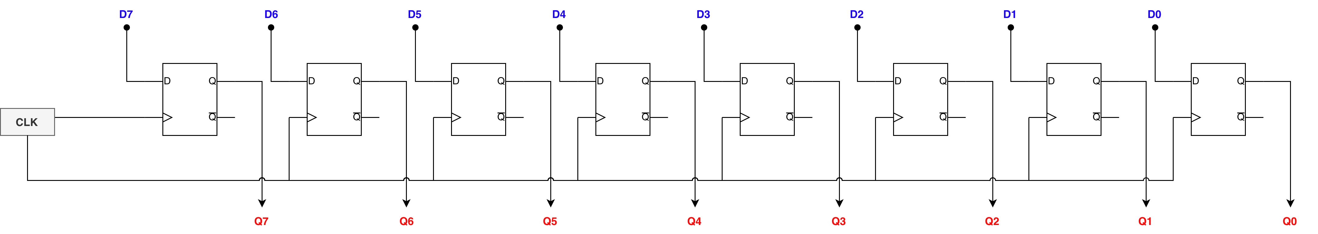
However Lucid simplifies this and make it 1-dimensional output instead of 8 by 1 array.
Adjust simulation clock rate and observe dff behavior
From the get-go, io_led[0] is flickering very rapidly because it displays the value of dff y that’s changing every clock cycle (of 1000Hz from the simulator). You can press pause as shown in the gif above and change the simulation clock rate to observe more visible changes on io_led[0], that is to increment the value in dff y slowly.
On the contrary, dff x is set to always maintain its value by connecting it’s d port to q port.
dff behavior you should observe:
- A
dffholds a value across clock cycles. - On each rising edge of the clock, it sample whatever’s plugged into its input port
.dand updates its output port.q. .clkand.rstshould normally be connected to the GLOBAL clock and reset (more reasoning on this later)- The
#INITparameter sets the initial andresetvalue of.q. - Arrays of
dffbehave as registers.
Capture values into dff
A common use case is to capture certain input state into a dff. For example, to store the state of current io_dip[0] when io_button[0] is pressed.
    io_led[0] = y.q // display y's output
    y.d = y.q // loop under normal circumstances
    if (io_button[0]){
        y.d = io_dip[0]
    }

Resetting dff
The rst port of a dff should be connected to the global reset signal because digital systems require a deterministic, known starting state during global reset.
When an FPGA powers up, internal registers may contain undefined values. Even though many devices perform an initialisation process, relying on that behaviour is poor design practice and reduces portability and predictability. By tying rst to a global reset source, all dff instances are driven to a known value at the same time.
This ensures that:
- ALL state elements start from a consistent baseline.
- The system behaves IDENTICALLY on every power-up.
- Debugging becomes reproducible, since your circuit does not depend on random startup states.
- Multi-register designs do not enter illegal or unintended states.
Equally important, a single global reset provides synchronisation of state across the entire design. Without this, different parts of the circuit might begin operating with unrelated internal values, producing unpredictable behaviour from the very first cycle.
Therefore, connecting the rst input of each dff to the global rst signal is not merely a convenience. It is a fundamental requirement for controlled and deterministic system behaviour. You can read this notes if you’d like more explanation.
If you’d like to set dff value to some initial value within your project, that’s simply writing a deterministic value to the dff and NOT a reset, as such:
    sig game_restart

    always {
        // logic to set game_restart

        io_led[0] = y.q // display y's output
        y.d = y.q // loop under normal circumstances
        if (game_restart){
            y.d = 0
        }
    }
A reset is a global system event. If you just need to zero-out a content of a particular dff, then that’s simply writing (state update).
Creating a Pipeline
Suppose you have the rca module from the previous lab, which you instantiate as an 8-bit adder.
You can connect the io_dips to its .a and .b port and manually observe its output at io_led. That approach is useful for quick verification, but it is not how real digital systems normally operate.
How real digital systems operate
In real systems, inputs are not provided manually, and outputs are not inspected continuously.
Instead, data (N bits) arrives as a time-ordered sequence, one set of values per clock cycle. Each set is sampled at a clock edge, processed, and then passed forward on the next edge. Remember, just like an assembly line. Real digital systems behave like a highly automated factory.
Although the
Nbit signals are parallel in space, they are serial in time.At any one instant in time, the system is handling N bits in parallel. That is spatial parallelism. Over successive clock cycles, those N-bit values arrive one after another. That is temporal serialism.
To support this behaviour, combinational logic is placed between registers (a block of dffs).
- The registers define pipeline stages.
- At each clock edge, a new input set enters the pipeline, and the result of the previous set moves to the next stage.
- Values are captured, held, and transferred forward only on clock edges.
This structure is known as a pipeline.
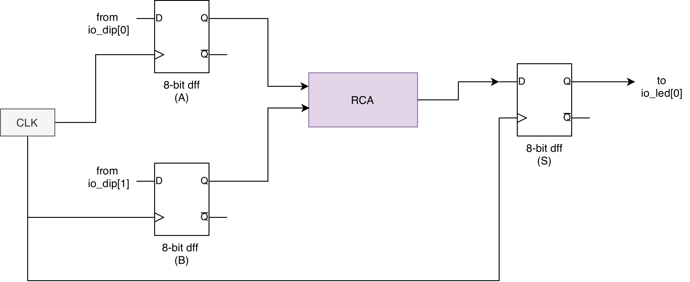
Simple Registered Adder
A simple registered adder behave as follows:
Input Register → Combinational Adder → Output Register
The registers act as time boundaries. They ensure that:
- New inputs are accepted only at defined instants
- The adder output has an entire clock period to settle.
- Only a stable, complete result is forwarded to the next stage.
We can build this easily in Lucid, following this arrangement:
    module registered_rca#(
        SIZE = 8 : SIZE > 0
    ) (
        input a[SIZE],
        input b[SIZE],
        output s[SIZE],
        input clk,
        input rst
        // optionally, you can have output cout port here
    ) {

        dff value_a[SIZE](.clk(clk), .rst(rst), #INIT(0))
        dff value_b[SIZE](.clk(clk), .rst(rst), #INIT(0))
        dff value_s[SIZE](.clk(clk), .rst(rst), #INIT(0)) // optionally, you can set this to have SIZE + 1 bits to include cout. We omitted it for this lab

        rca rca(#SIZE(8), .a(value_a.q), .b(value_b.q), .cin(0)) // edit the ports yourself to suit your rca's interface

        always {
            s = value_s.q

            value_a.d = a
            value_b.d = b
            value_s.d = rca.s

        }
    }
Test
Test using a very slow clock
To observe that the registers provide an orderly-fashioned output, you will need to simulate it with slower clock, like 1Hz.
In alchitry_top, instantiate this registered_rca, and also the combinational logic rca. To make a toy slow clock, we use a component called counter (you can import it from the component library, under miscellaneous category). Then connect the display to the two LED rows:
The counter component is used here simply as a toy frequency divider to slow the system clock down to a human-observable rate. It is roughly slowed down to 1Hz (as opposed to 1000Hz) for testing purposes only. Give the appendix a read if you’re not familiar with the concept of frequency divider.
    counter slow_clock(#DIV(9), .clk(clk), .rst(rst), #SIZE(1))

    // FOR DEMO PURPOSES ONLY in SIMULATOR: we connect .clk port of registered_rca to slow_clock
    registered_rca rr(#SIZE(8), .a(io_dip[0]), .b(io_dip[1]), .clk(slow_clock.value), .rst(rst))
    rca rca(.a(io_dip[0]), .b(io_dip[1]))

    always {

        io_led[0] = rr.s
        io_led[1] = rca.s
    }
The goal is to observe that with slower clock, we see that the output shown in io_led[0] is periodic and consistent, synchronized to the slow clock’s frequency. This is akin to a consistent display “refresh rate”. However, the output in io_led[1] depends on the input, that is manually controlled and unpredictable (does not get refreshed at a constant rate).

Observation 1: Unregistered inputs between clock edges
In a clocked system, only the value that exists at the sampling edge matters. Any changes that occur in between edges are intentionally ignored. This is not a flaw. It is the entire design principle of a digital system.
You can think of it like a camera taking one photograph per second.
- Movements between photos may be interesting, but they are not recorded.
- The system only commits to what is visible at the instant the picture is taken.
Similarly, a dff only captures what is present at the edge of the clock. Everything else is transient and deliberately discarded. This is what makes behaviour consistent and repeatable.
Observation 2: Periodic and Synchronized Output Suitable for Downstream Components
Like what we have learned in lecture, the registered adder produces an output that is:
- Time aligned to a known reference: the clock
- Stable for a full period
- Independent of how noisy or irregular the input activity is in between edges
This kind of output is essential when the result is used by another clocked block, which expects it to be stable, for example: if you add a comparator block after the registered adder block to post-process the adder’s result.
In contrast, the unregistered adder reacts immediately to every change in the input. That makes it appear more “responsive” but it is actually unreliable and unsynchronised. Its output cannot be reliably consumed by other logic without additional timing control.
Clock speed in practice
In practice, we use a clock frequency fast enough to make the unit appear responsive, for example: 100MHz as provided by default in Alchitry Projects.
As mentioned in the intro, can synthesize faster clocks (>100Mhz) using Vivado Clock Wiz, provided that it obeys the dynamic discipline.
(Important) Demo Code Warning
The test code above connects the .clk port of the registered_rca into the slow_clock data output for demo purposes only:
    counter slow_clock(#DIV(9), .clk(clk), .rst(rst), #SIZE(1))

    // FOR DEMO PURPOSES ONLY in SIMULATOR: we connect .clk port of registered_rca to slow_clock
    registered_rca rr(#SIZE(8), .a(io_dip[0]), .b(io_dip[1]), .clk(slow_clock.value), .rst(rst))
NEVER do this in real projects. You should always connect the global clock from alchitry_top as .clk input to all components in your project. Read the “one clock to rule them all” section above again if you are unclear.
    // clk comes from alchitry_top
    registered_rca rr(#SIZE(8), .a(io_dip[0]), .b(io_dip[1]), .clk(clk), .rst(rst))
If you really need to “slow down” the dffs in the adder for specific purposes, you should do one of these two things:
- Generate slower clock using Vivado Clock Wiz and use it in your project.
- Use the frequency divider’s output as an
enablesignal to thedffin yourregistered_adder(see below)
Button-controlled Sampling
In the previous section, your registered RCA updated periodically using a slow clock. We now introduce a slightly different but very natural variation: the register will only update when an enable button is pressed.
This lets you control exactly when the state of the dip switches is captured.
Register with Write Enable signal
You can create an N bits reg module with en (enable) signal. We sample new input at the nearest next edge only when en is high, but maintain old value otherwise.
    module reg_en#(
        SIZE = 1: SIZE > 0,
        INIT = 0
    ) (
        input clk,  // clock
        input rst,  // reset
        input en,
        input d[SIZE],
        output q[SIZE]
    ) {
        dff regs[SIZE](#INIT(INIT), .clk(clk), .rst(rst))
        always {
            regs.d = regs.q
            if (en){
                regs.d = d
            }
            q = regs.q
        }
    }
The reg_en module behaves like a regular dff if en is always set to 1. Formally, this is called a “register with write enable”. You will see more of these in the later weeks when we learn about Datapath.
Registered Adder with Enable
Then we can use reg_en module to create the following registered adder with enable:
module registered_rca_en#(
    SIZE = 8 : SIZE > 0
) (
    input a[SIZE],
    input b[SIZE],
    output s[SIZE],
    input enable,
    input clk,
    input rst
    // optionally, you can have output cout port here
) {

    reg_en value_a(.d(a),.clk(clk), .rst(rst), #INIT(0), #SIZE(SIZE), .en(enable))
    reg_en value_b(.d(b),.clk(clk), .rst(rst), #INIT(0), #SIZE(SIZE), .en(enable))
    reg_en value_s(.clk(clk), .rst(rst), #INIT(0), #SIZE(SIZE), .en(enable)) // optionally you can set value_s as SIZE+1 to consider cout too

    rca rca(.a(value_a.q), .b(value_b.q))

    always {
        s = value_s.q
        value_s.d = rca.s

    }
}
For this lab, we simplify and omit cout in registered_adder_en module. You can choose to include it if you wish. It will not affect your checkoff.
Capture signal with io_button
When instantiating this module, you can connect one of the io_button to the enable signal.
    // alchitry_top
    registered_rca_en rr_en(.a(io_dip[0]), .b(io_dip[1]), .clk(clk), .rst(rst),.enable(io_button[0]))

    always {

        // other connections
        io_led[2] = rr_en.s
    }
The following shows that the new button-triggered adder will be fed with new input only when io_button[0] is pressed:

Capture signal with slow_clock as enable:
You can also achieve the same “slow down” effect like the test demo above by passing slow_clock signal through an edge_detector, and using it as the enable signal for this adder:
    counter slow_clock(#DIV(9), .clk(clk), .rst(rst), #SIZE(1))

    registered_rca_en rr_en_with_slowclock(.a(io_dip[0]), .b(io_dip[1]), .clk(clk), .rst(rst),.enable(slow_clock.value))
This keeps everything clocked on the true 100 MHz clock while still slowing down when the adder captures new inputs.
Note that using slow_clock.value directly as an enable means the adder will update for multiple consecutive 100 MHz cycles as long as slow_clock is high (see diagram below), not just once per slow clock period. If you want it to update exactly once per slow clock rising edge, you will need an edge_detector, which we will cover in the next lab.

Notice also the “slight delay” of the slow_clock signal indicated by the green shade in the diagram above. Since slow_clock is generated by a frequency divider driven by 100 MHz, its output transitions happen slightly after a default clk (100 MHz) rising edge, not exactly at the same time.
So at some time t, the 100 MHz edge fires first, the counter increments, and slow_clock.value changes a short time after that due to clock-to-q delay (tpd). Therefore, there’s no violation of dynamic discipline here.
The slow_clock.value being derived from the same 100 MHz counter is the key: its edges are always slightly after a 100 MHz edge, never exactly on one. This further stresses the importance that all components in your system should be driven by the same clk source.
Here’s a demo gif to show you the “effect” of using slow_clock.value as enable signal:

When io_dip is changed (a and b values) as:
slow_clock.value = 0, the output atio_led[2]is not updated until the next timeslow_clock.value = 1.slow_clock.value = 1, the output atio_led[2]will be updated at eachclkrising edge (e.g: 1000Hz in simulator, or 100Mhz in hardware)
Testbench
Before testing hardware on the FPGA, digital designs are almost always verified in simulation, just like how software is tested before deployment. A testbench plays the role of a small “driver program” that:
- Feeds known inputs to the design,
- Advances time under full control of the simulator,
- And checks whether the outputs match what they should be.
This mirrors how you would test a function in software by calling it with test cases and checking the returned value. The difference is that in hardware, results do not appear immediately: they emerge only after the correct number of clock cycles, and the testbench must account for that explicitly.
Your senior wrote a detailed handout on how testbench works in Alchitry. Give it a read before proceeding.
Creating a Basic Test File (Combinational)
To begin, create a new Lucid Test Bench. A new file is typically needed per module you wish to test.
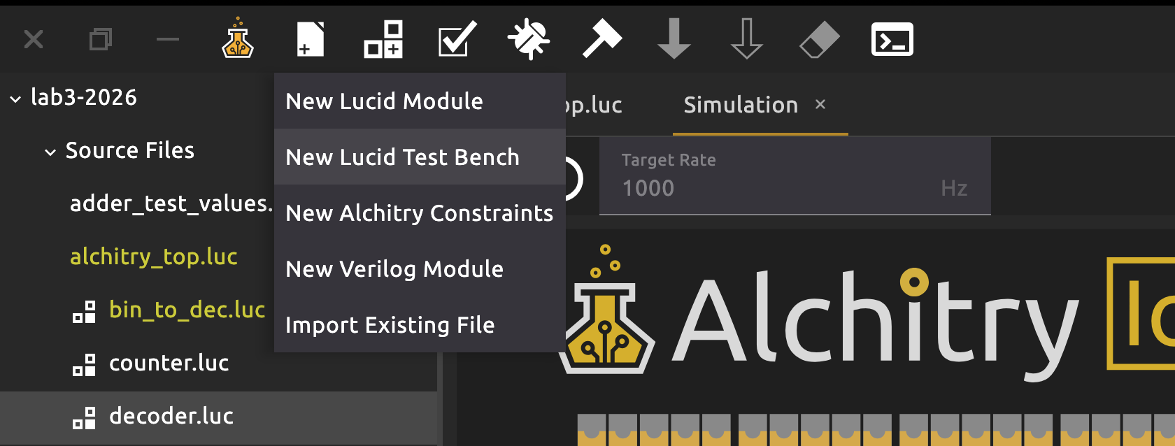
Inside a testbench, you can define test blocks using the test keyword. Here’s a minimal test file for your combinational logic rca (without registered adder).
testbench test_rca {
sig clk
rca adder // module declaration
fun tick_clock() {
clk = 1
$silent_tick() // tick without capturing signals
clk = 0
$tick()
}
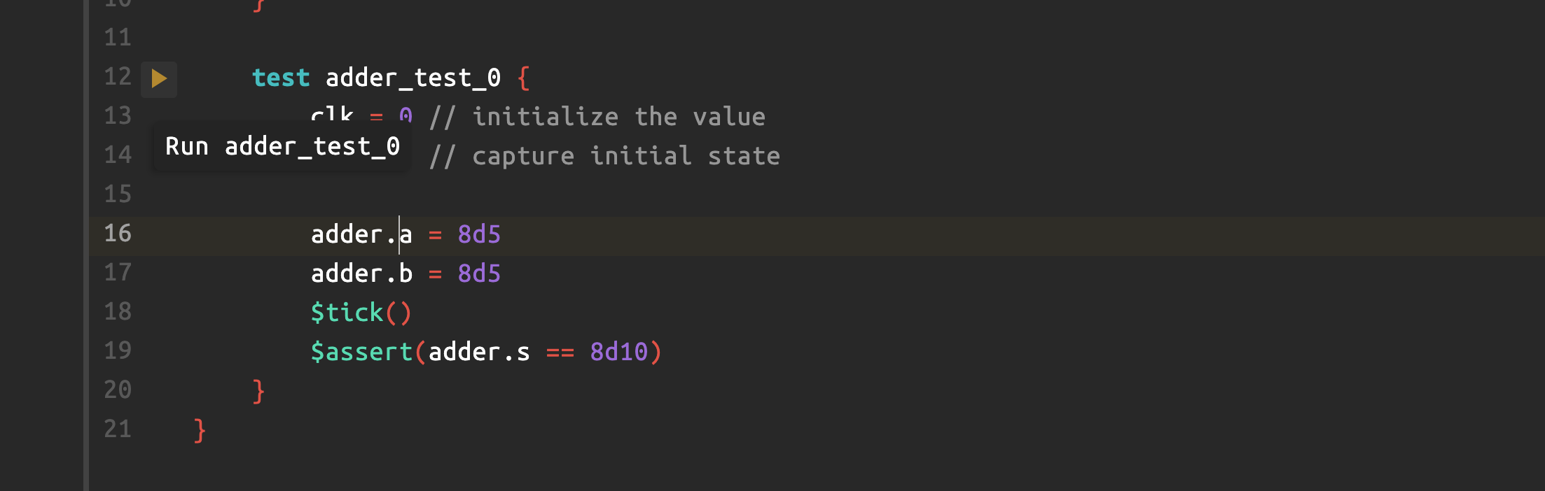
test adder_test_0 {
adder.a = 8d5
adder.b = 8d5
$tick() // capture state
$assert(adder.s == 8d10)
$print("First test case -- a: %d, b: %d, c:%d", 8d5, 8d5, adder.s)
}
}
Here you supply test value of a and b, then call $tick to propagate signals. Finally, we call the $assert function to ensure that the value of the adder’s sum is equal to your test case.
If everything goes well, you should see a “play” button beside your test description. Click it to run the test:
A waveform window should appear and plot signal values at the time of $tick:
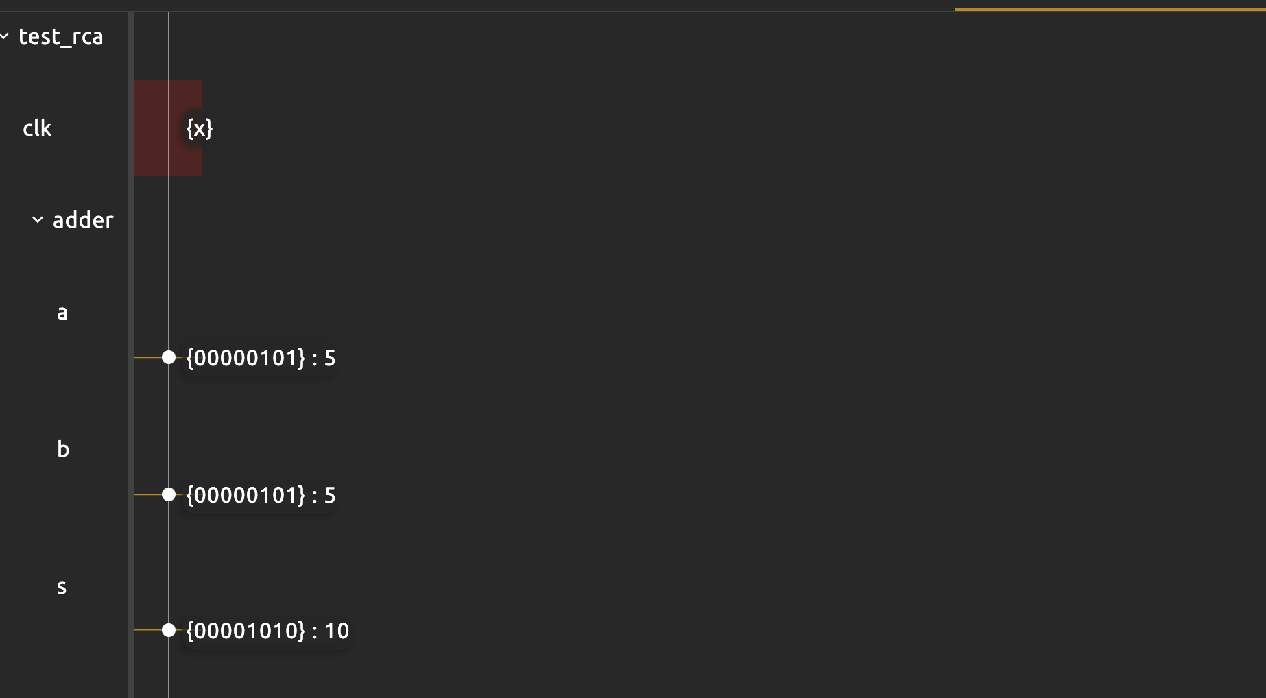
This waveform window prints out the states of all ports declared in that test block in terms of {binary}:decimal value. The sig clk is x because we didnt set or use it in this test.
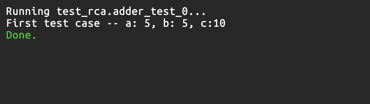
If you wish, you can print the signals as well as shown above. You should see the following output in the console:
Creating other test cases
What if you want to make another test case? While you can write another test block with differing values, you can also change a and b values after each tick. Here’s an example to illustrate that:
    test adder_test_1 {
        adder.a = 8d5
        adder.b = 8d5
        $tick()
        $assert(adder.s == 8d10)
        $print("First test case -- a: %d, b: %d, c:%d", 8d5, 8d5, adder.s)

        adder.a = 8d1
        adder.b = 8d3
        $tick()
        $assert(adder.s == 8d4)
        $print("Second test case -- a: %d, b: %d, c:%d", 8d1, 8d3, adder.s)
    }
The waveform window will now report the two value set:

tick Propagates Signals
tick function propagates signal and capture it. You can read further docs here. Without it, you cannot feed different test values into the combinational-logic adder. For instance, the following test case fails:
    test invalid_test {
        adder.a = 8d5
        adder.b = 8d5
        $assert(adder.s == 8d10)
        adder.a = 8d1
        adder.b = 8d3
        $assert(adder.s == 8d4)
    }
This fails because $assert checks the current stable state. Since we never call $tick between changes, the simulator never propagates the new input into adder.s.
Testbench with a dff
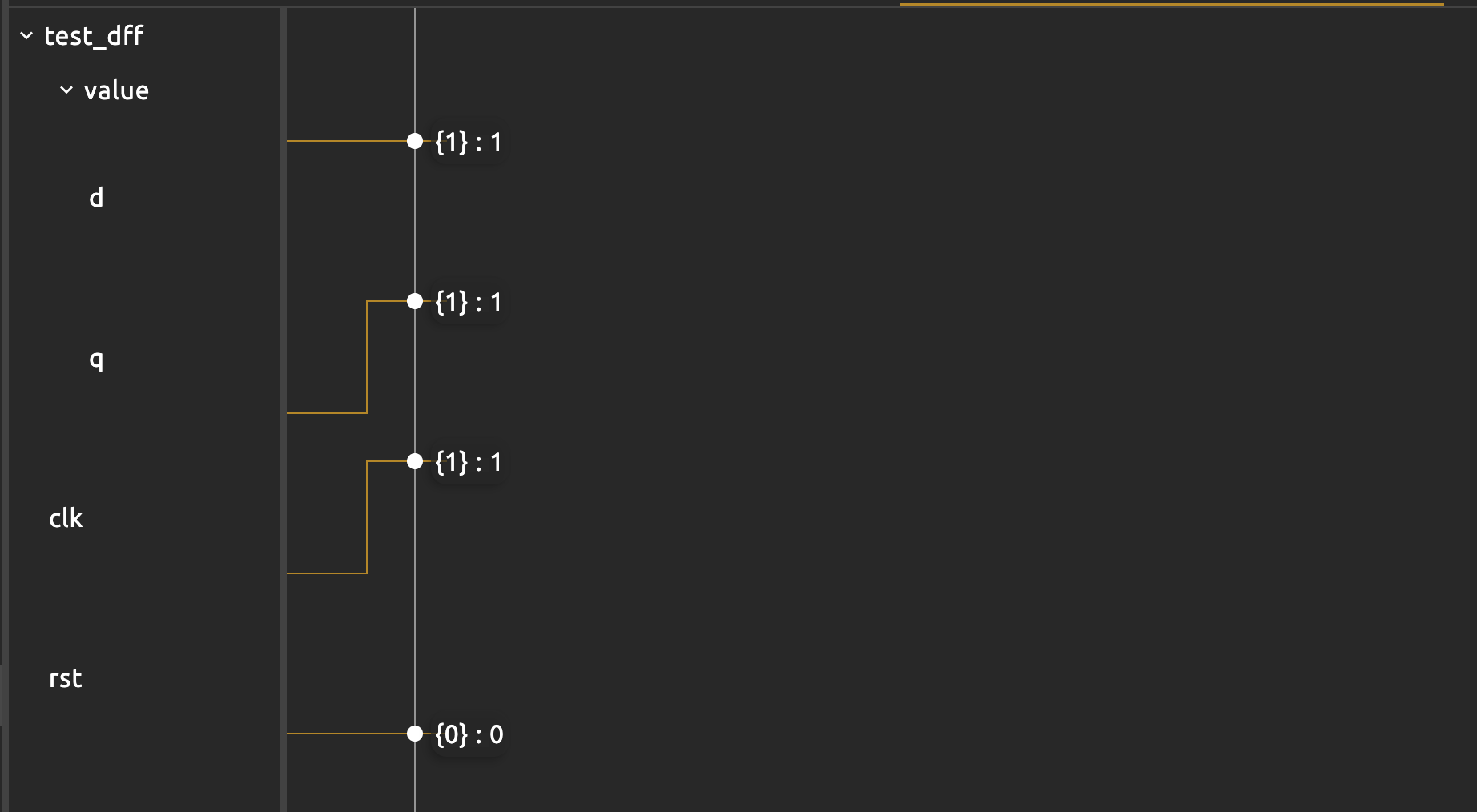
You need to propagate clk =0 and clk=1 to allow a dff to latch. For example, value.q remains 0 here when we print it out and run the test case:
    sig rst
    dff value(.clk(clk), #INIT(0), .rst(rst))
    test value_propagate{
        clk = 0
        rst = 0
        value.d = 1
        $tick()
        $print("value.q: %d", value.q)
    }
You need to propagate a rising edge so that we have a 1 outputted at value.q:
    sig rst
    dff value(.clk(clk), #INIT(0), .rst(rst))
    test value_propagate{
        clk = 0
        rst = 0
        value.d = 1
        $tick()
        $print("value.q: %d", value.q)

        clk = 1
        $tick()
        $print("value.q: %d", value.q)
    }
The waveform clearly illustrates this: that the .q port of the dff “captures” the input (at .d) when the clock rises.
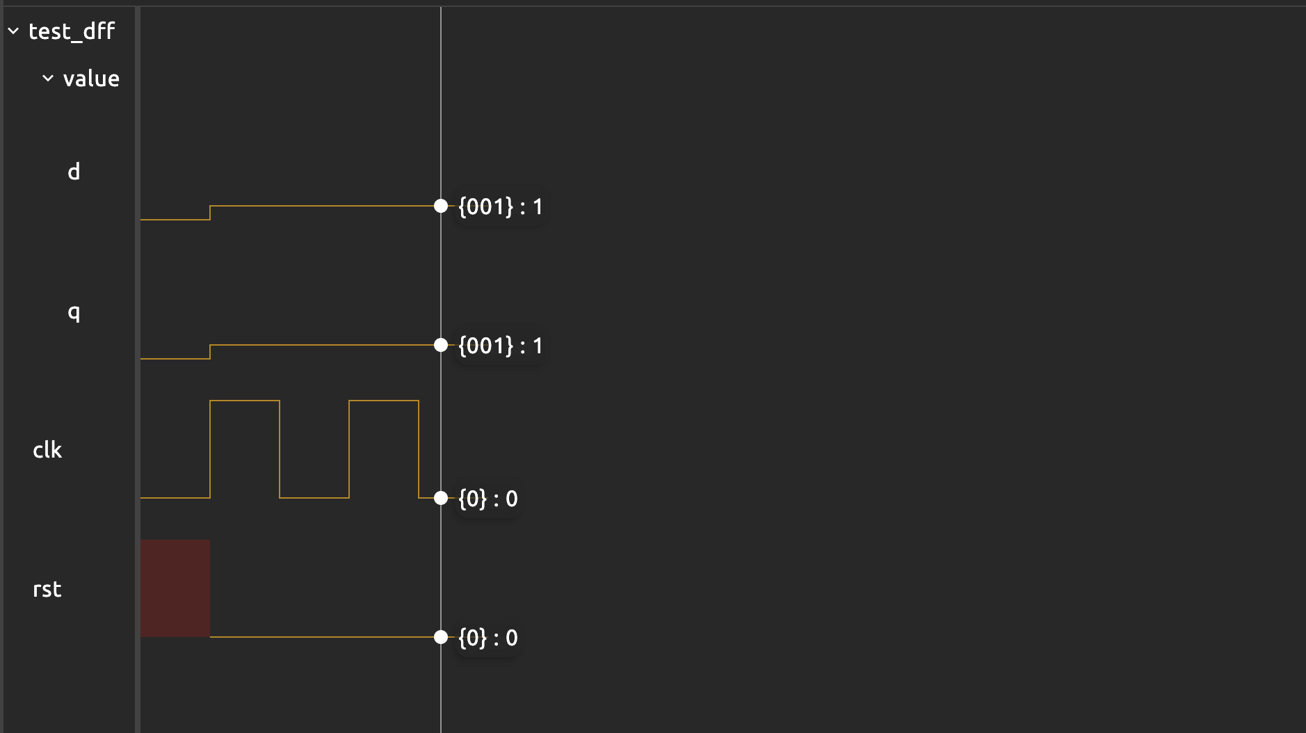
To make things neater, you can write a function with fun keyword that sets clk and tick accordingly. This makes it reusable:
    fun tick_clock_rising(){
        clk = 0
        $tick()
        clk=1
        $tick()
    }

    test value_propagate_v2{
        rst = 0
        value.d = 1
        $tick_clock_rising()
        $print("value.q: %d", value.q)
    }
The given $tick_clock in the test template sets the clk to 1 and perform $silent_tick instead, then sets clk back to 0. The waveform therefore didn’t plot changes at rising edge but only on falling edge. We find this to be slightly confusing, so it might be better to write your own clock function as above to see the full plot.
test block is NOT always block
The
testblock works sequentially, UNLIKE thealwaysblock.In a test block, there is no always block running every cycle. The test body runs once, top to bottom, like a little program. If you want a signal to change over time, you must:
- Assign it a new value in the test code,
- Advance time with
$tickor your clock helper,- Then assign again and tick again.
A
repeatloop is also sequential: on each iteration it executes the statements inside, then moves on.
For instance, this will not set .q to be 2 after running because you didn’t change the assignment to .d after the first $tick_clock():
    sig rst
    dff value[3](.clk(clk), #INIT(0), .rst(rst))

    test value_increase_fail{
        clk = 0
        $tick()

        rst = 0
        value.d = value.q + 1

        $tick_clock()
        $tick_clock()
    }
If you’d like to increment the value of the dff and advance two clock cycles, you need to write a loop so that we call $tick_clock each time we change value.d:
    sig rst
    dff value[3](.clk(clk), #INIT(0), .rst(rst))

    test value_increase{
        clk = 0
        $tick()

        rst = 0
        repeat(2){
            value.d = value.q + 1
            $tick_clock()
        }
    }
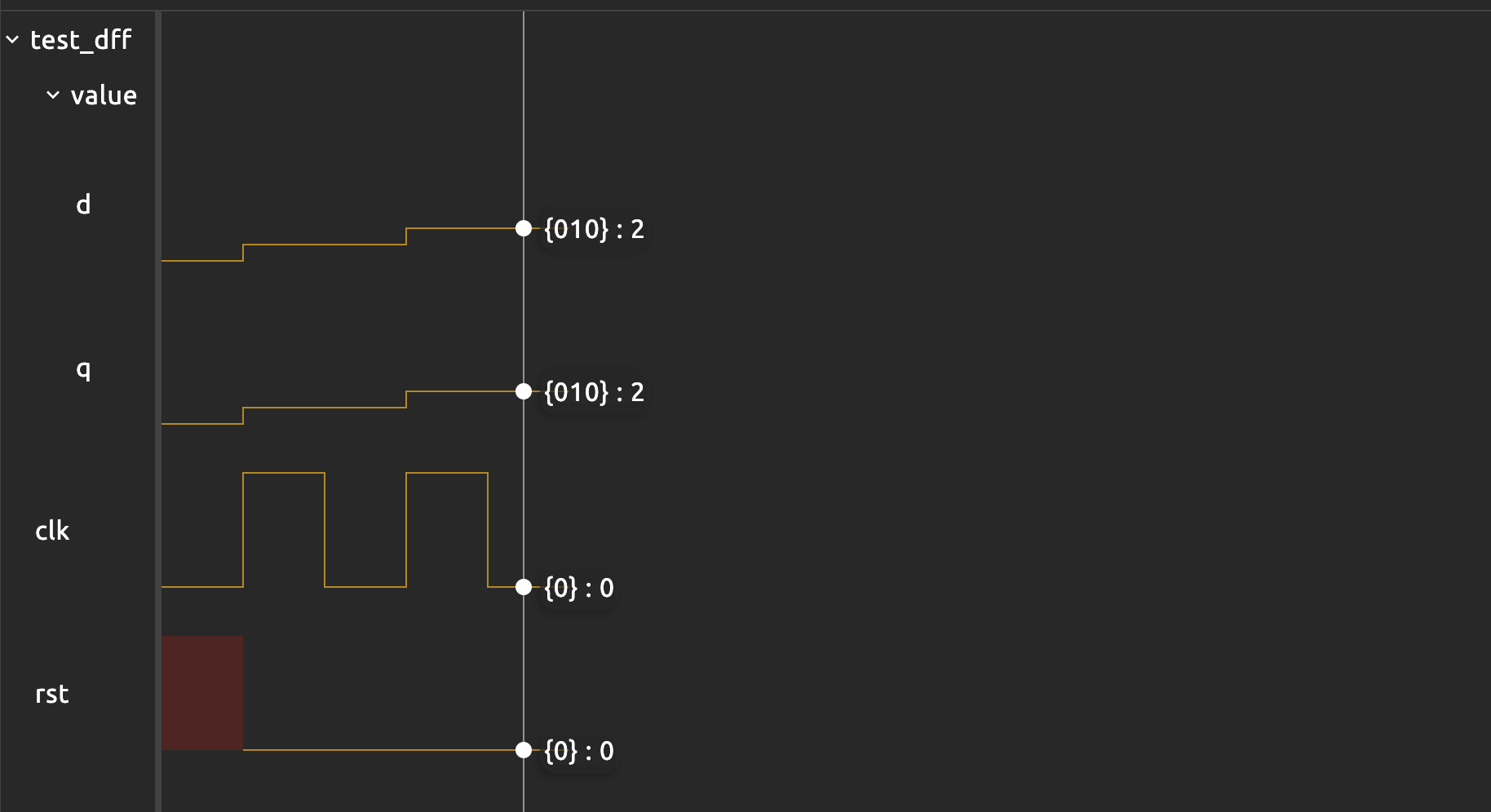
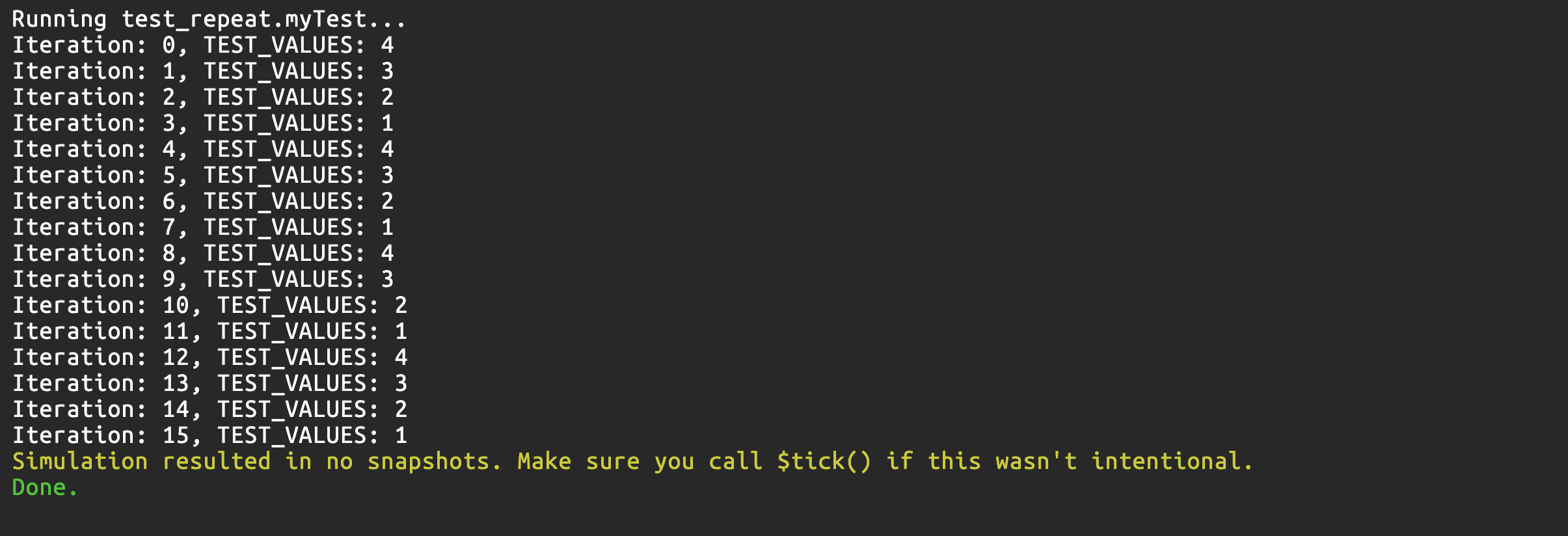
The repeat loop also runs sequentially, just like a regular for loop. This example demonstrates it:
    const TEST_VALUES = {
        8h1,
        8h2,
        8h3,
        8h4
    }

    test myTest {
        repeat(i, 16){
            $print("Iteration: %d, TEST_VALUES: %d", i, TEST_VALUES[i[1:0]])
        }
    }
Checkoff
Testbench for Registered Adder (2%)
Write a testbench to test the functionality of your registered adder. Your test case should have an automatic $assert as well as printouts for easy access. The waveform should clearly show what happens within the module. For instance, here’s a demo.
You must also be able to clearly explain the waveforms and notice the delays (2 clock cycles) between test case input and the corresponding sum output from the registered adder (see section below).

Declaring Test Vectors (Separate Arrays vs Bitpacked)
There are two acceptable ways to store the test cases for the adder:
Separate Constant Arrays
const A_INPUTS = {8h00, 8h01, ...}
const B_INPUTS = {8h00, 8h01, ...}
const SUMS     = {8h00, 8h02, ...}

a = A_INPUTS[index]
b = B_INPUTS[index]
expected = SUMS[index]
This is easy to read. Each array has a clear meaning but you must keep all three arrays aligned by index. It may seem tedious but pretty simple to do if you ask an AI to generate one for you.
Bitpacked 24-bit Records
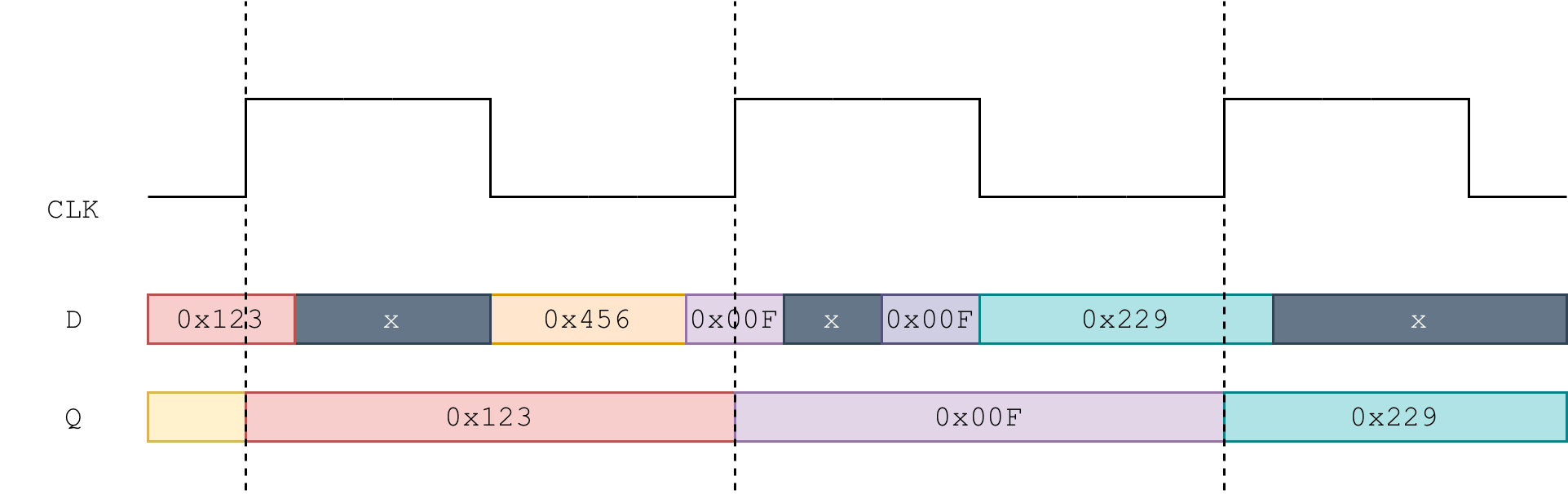
Each entry is {a[7:0], b[7:0], s[7:0]}.
const TEST_VALUES = {
  24h010102, // a=01, b=01, s=02
  24h0F0110, // a=0F, b=01, s=10
  ...
}

a = TEST_VALUES[index][23:16]
b = TEST_VALUES[index][15:8]
expected = TEST_VALUES[index][7:0]
Each test case is stored as one record, so alignment errors are impossible. It is more elegant since it matches how real datapaths often store multiple fields in a single word. Slightly harder to read, but more compact and structurally robust.
In this lab, both formats are acceptable. Use separate arrays if you want clarity; use packed 24-bit records if you want a single self-contained entry per test case.
Recall: array indexing is just bit selection
In HDL, if you do
TEST_VALUES[0], you are doing bit selection. This means select the lowest “bit” or “unit”. In this case, you will not get the first element you wrote in the definition ofTEST_VALUES, but the last instead.For example, if we have
const TEST_VALUES = {24hAB, 24hBC}, thenTEST_VALUES[0]gives24hBCinstead.
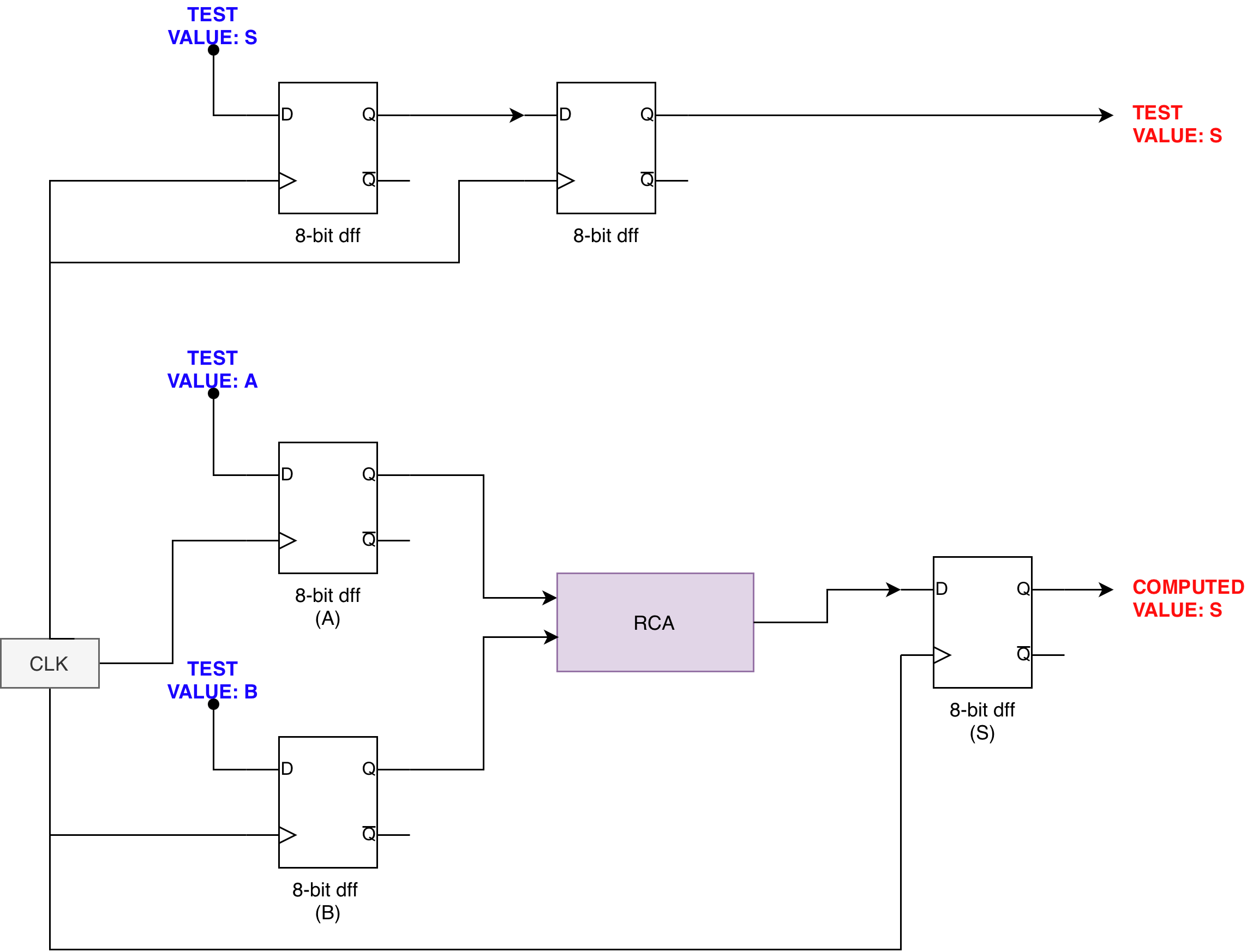
Matching Latency in the Tester
Our registered adder has registers at both the inputs and the sum output. From the testbench’s point of view, this means:
- At clock edge
k: the testbench presents (a, b) and they are about to be sampled to the input registers (present at thedports) - During cycle
ktok+1: (a,b) are captured (sampled) into the input regs and the combinational adder computes the sum. - At clock edge
k+1: the result is captured (sampled) into the output register. - At clock edge
k+2: that result is visible and stable at the module’s s port.
So the sum that you see at time k+2 belongs to the inputs that were applied at time k. This diagram illustrates that:
Your testbench must respect this 2-cycle latency.
There are two reasonable ways to do it.
Sequential Way
This is the simplest way.
For each test case:
- Set
aandbto the next test vector. - Tick the clock twice using
tick_clock_risingto let the value travel through the two register stages.- If you use the default
tick_clock, then call it thrice, as this is a falling edge
- If you use the default
- Then compare the registered sum with the expected value.
Here’s a template:
    // declare your device under test here (dut)

    const NUM_TESTS = ...
    const A_INPUTS = {8h00, 8h01, ...}
    const B_INPUTS = {8h00, 8h01, ...}
    const SUMS     = {8h00, 8h02, ...}

    test registered_rca_basic {
        clk = 0
        rst = 1
        $tick()          // reset
        rst = 0


        repeat(i, NUM_TESTS) {
            // 1. Apply inputs for test i
            dut.a = A_INPUTS[i]
            dut.b = B_INPUTS[i]

            // 2. Advance two clock cycles
            $tick_clock_rising()
            $tick_clock_rising()

            // 3. Now the output corresponds to A_INPUTS[i], B_INPUTS[i]
            $assert(dut.s == SUMS[i])
            $print("Test %d OK --- s: %d, answer key s: %d",i, rr.s, test_values.s)
        }
    }
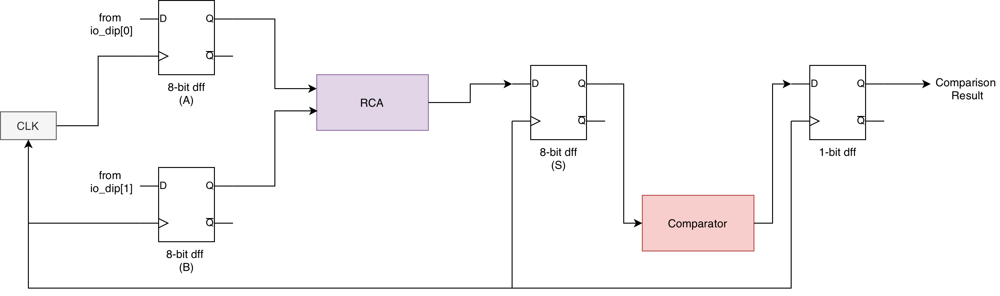
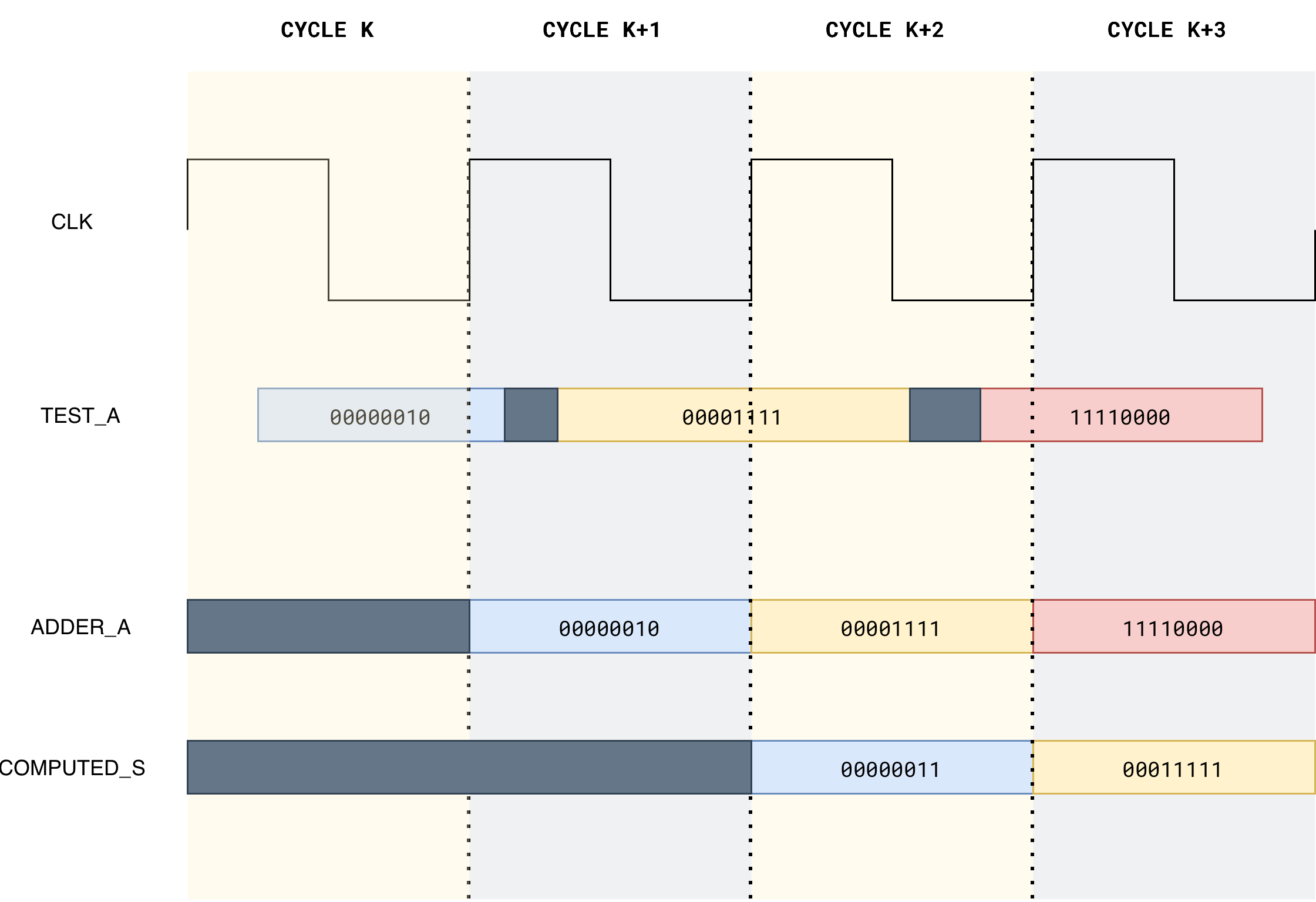
Pipelined Way
If you want to mirror how a real hardware tester would behave, you can keep feeding new test vectors every cycle and maintain a small pipeline of expected sums inside the testbench. In each cycle we:
- Apply a new (
a, b) pair. - Push the corresponding expected_sum into a 2-cycle delay line in the testbench.
- Tick the clock once.
- After the first two “warm-up” cycles, the oldest value in this delay line lines up with the current
dut.s.
The diagram below illustates the arrangement:
We pass the test value S through the same number of registers as test value A and B. This reinforces a key principle in clocked design: You can only compare signals that have passed through the same number of clock boundaries.
Checkoff Summary
You should show your registered adder testbench design to the TA and run it in Alchitry Labs.
- (0.5%) You should use
$assertkeywords to automatically check if the adder’s answer match the answer key - (0.5%) You should have at least 8 different test cases: check all edge cases such as overflow, addition with zeros, etc
- (1%) TAs will ask you two questions (same protocol as lab 2) about the waveforms, ensure that you understand how the waveform works
Schedule a checkoff with your TA anytime before the end of next week’s lab as a 1D group. The checkoff is graded individually but to aid logistics and to ensure everyone in the group is on the same page, you are required to attend the checkoff together as a 1D group. It will take about 15 minutes in total for the whole group to clear a checkoff on average.
Summary
In this lab, you shifted from thinking about circuits as “instantaneous” combinational blocks to seeing them as clocked machines that move forward one step at a time.
The clock and dffs define clear time boundaries: values are sampled on an edge, held for a full period, and only then passed to the next stage.
- Using these building blocks, you built a registered RCA, observed how its output becomes periodic and synchronised, and contrasted it with an unregistered adder that responds immediately (and unreliably) to input flicker.
- You extended the idea with registers that have enable signals, allowing inputs to be captured only when a button is pressed.
For checkoff, you then constructed a testbench to test the functionality of your registered adder:
- Store test vectors in constants,
- Step through them sequentially in the testbench over multiple clock cycles,
- Compare the registered adder output with expected sums using
$assert.
Although subtle, we also learned how to match latency: since the registered adder output is delayed by two clock boundaries from the tester’s point of view, the expected sum must be delayed by the same number of stages before comparison.
The new values of value_a.q, value_b.q, and value_s.q therefore appear one 100 MHz period later, which is 10 ns after the slow clock edge.
This means the output s does not update exactly at the slow clock edge but 10 ns after it. In most designs this is completely inconsequential since the slow clock period is orders of magnitude larger, for example 20 ms for a 50 Hz slow clock. But it is worth being aware of if you are building something that has tight dependencies between the slow clock edge and when downstream logic reads the output. For this lab, it does not affect the output you see or your design.
Appendix
Frequency Divider
A frequency divider is a circuit that generates a slower clock signal from a faster one.
If the input clock has frequency \(f\), a divider produces an output clock with frequency \(\frac{f}{N}\), where \(N\) is called the division factor.
In digital systems, this is commonly implemented using a counter (a bank of D flip-flops):
- Each bit of an incrementing counter toggles at a different rate.
- Bit
0toggles at \(\frac{f}{2}\) - Bit
1toggles at \(\frac{f}{4}\) - Bit
2toggles at \(\frac{f}{8}\) - Bit
ntoggles at \(\frac{f}{2^{n+1}}\)
By selecting one of these bits as a new clock signal, the original frequency is effectively divided. The figure below illustrates how frequency division works. You can connect these flip flops in series to further divide the frequency by powers of 2.
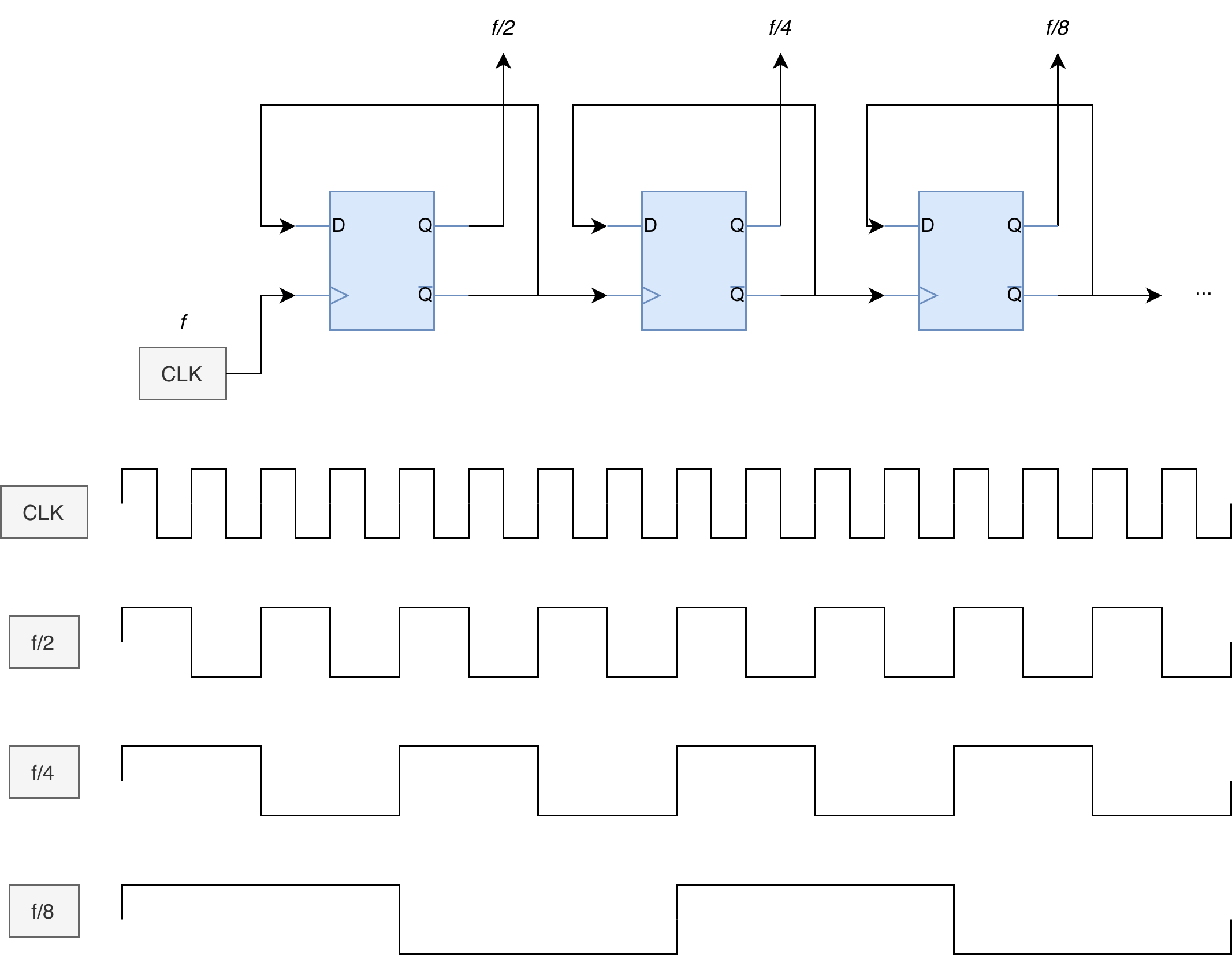
The Lucid equivalent code for the above arrangement is:
    .rst(rst){
         dff f_2(.clk(clk))
         dff f_4(.clk(~f_2.q))
         dff f_8(.clk(~f_4.q))
         // define more as needed
    }

    always {

        f_2.d = ~f_2.q
        f_4.d = ~f_4.q
        f_8.d = ~f_8.q

        // use f_x.q as needed
    }
Unfortunately, you cannot use the repeat loop to automatically instantiate the dff since Lucid requires its clk connection to be defined outside of the always block, and repeat procedure is only valid inside always block.
Therefore this lab, we simply use counter library component to act as a black-box frequency divider whose only purpose is to slow the FPGA’s clock down to a rate that is observable to the human eye.
Frequency Divider via a Binary Counter Bit Tap
If you don’t like to use the counter like a black box, we also create our own simple frequency divider by building a DIV-bit synchronous binary counter out of D flip-flops and then using one counter bit as the output clock.
module frequency_divider#(
    DIV = 1: DIV > 0
) (
    input clk,  // clock
    input rst,  // reset
    output out
) {
    dff counter[DIV](.clk(clk), .rst(rst))
    always {
        counter.d = counter.q + 1
        out = counter.q[DIV-1]
    }
}
It does the following:
dff counter[DIV]is a register bank:DIVDFFs storing aDIV-bit valuecounter.q.counter.d = counter.q + 1means the register increments by 1 every clock edge (synchronous counter).out = counter.q[DIV-1]is just a wire tap to one bit of the counter register. No extra timing logic is created foroutbeyond the flip-flops already in the counter.
A binary counter like this has this toggling pattern:
counter.q[0](LSB) toggles every clock tick → output frequency = clk / 2counter.q[1]toggles every 2 ticks → clk / 4counter.q[2]toggles every 4 ticks → clk / 8- In general,
counter.q[k]toggles at clk / 2^(k+1)
So when we set out = counter.q[DIV-1], we get out frequency = clk / 2^DIV.
Example: DIV = 3 taps q[2], so out = clk / 8.
This method naturally gives a 50% duty cycle for divides by powers of two.
The counter width must be at least
DIVbits so thatcounter.q[DIV-1]exists; using exactlyDIVbits is the minimal, clean implementation.If you need a non power-of-two divide (÷3, ÷10, etc.), you typically use a mod-N counter and explicit toggle/compare logic instead of a single bit tap.
This counter-bit method is just a neat way to produce a frequency divider: instead of thinking “chain DIV flip-flops,” we think “make a DIV-bit counter and tap bit DIV−1,” and that tapped bit has the same divided frequency.
The output of this frequency divider, whether from a chained DFF or a counter bit tap, is a data signal routed through general fabric. It must NEVER be used as a clock pin for any downstream module, especially BRAMs. Use it only as input to an edge_detector or as a synchronous enable. See Custom Clock Pitfall for a full explanation of what goes wrong when you do.