 50.002 CS
- Preface
dffin Verilog- A Deeper Dive into Verilog’s Blocking and Nonblocking Assignments
- What Verilog “implies” to tool
- Testbench
- Creating a Pipeline
- Testbench Design
- Decide what is “procedural state” vs “driven by hardware”
- Parameterize the testbench so it matches multiple DUT sizes
- Precompute vectors as an answer key
- Create pipelined delay registers for the answer values
- Pay attention to any
ensignals and asyncresetused in DUT - Clock generation and
negedge - Pipeline fill and drain
- Compare with case inequality and count errors
- Reset sequencing and enabling
- Sample Waveform Output
- Summary Approach
- Frequency Divider
- Conclusion
- Appendix
50.002 Computation Structures
Information Systems Technology and Design
Singapore University of Technology and Design
(Verilog) Lab 3: Clocked Circuits
This is a Verilog parallel of the Lucid + Alchitry Labs Lab 3. It is not part of the syllabus, and it is written for interested students only. You still need to complete all necessary checkoffs in Lucid, as stated in the original lab handout.
If you are reading this document, we assume that you have already read Lab 3 Lucid version, as some generic details are not repeated. This lab has the same objectives and related class materials so we will not paste them again here. For submission criteria, refer to the original lab 3 handout.
Preface
Real systems need order in time. They must perform one step, then the next, then the next, in a controlled and repeatable way so that ALL components progress together and remain synchronized. To achieve this, we introduce a clock.
In this lab, we will use dffs to construct registers and create our first clocked circuits called the pipelined RCA. With this, we should begin to see our design not as a collection of gates, but as a machine that moves forward one step at a time, on each clock edge.
Although many signals may exist in parallel, the system progresses in a sequence of moments. A clock’s function is to divide (continuous) time into uniform periods and creates discrete moments when a circuit is allowed to change its state.
Each clock edge represents ONE new state in the system, e.g: new set of input values fed to the system, new set of output values produced by the system, etc.
This way of thinking will form the basis of state machines in the next lab.
dff in Verilog
As you’ve learned in lecture, a dff commonly has 3 ports: a data input that defines the next state (D), a timing control
input that tells the flip-flop exactly when to “memorize” the data input (CLK), and the output port (Q). Sometimes it has three extra ports:
ResetorCLR(input): it can cause the memory to be reset/cleared to0regardless of the other two inputs (D and CLK). This is also known as asynchronous resetEN(input): when high,Dis captured at risingCLKedge, otherwise it retains its old value~Q(output): simply the inverse ofQ’s value
The diagram below shows the variation with reset (clear) and with enable + reset:
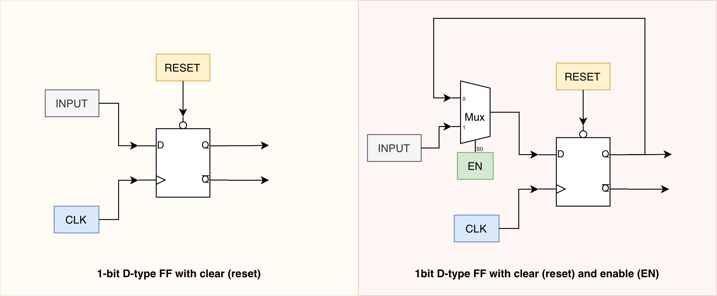
The implementation in Verilog is straightforward. Note that in here, we use the non-blocking assignment (<=) and always @posedge clk now, to synthesize sequential logic. This is different from the usual blocking assignment and always @* we previously used to implement combinational logic.
module dff(
    input D,
    input clk,
    input rst,
    output reg Q
    );

always @ (posedge clk or posedge rst)
begin
    if (rst == 1)
        Q <= 1'b0;
    else
        Q <= D;
end

endmodule
If you’d like an en signal, you may explicitly use a procedural variable to hold the old_Q and choose assignment:
module dff_en(
    input  D,
    input  clk,
    input  rst,
    input  en,
    output reg Q
);

reg next_Q;

// combinational
always @* begin
    next_Q = Q;          // default: hold
    if (en) next_Q = D;  // if enabled: take D
end

// sequential
always @(posedge clk or posedge rst) begin
    if (rst) Q <= 1'b0;
    else     Q <= next_Q;
end

endmodule
However in practice, the following implementation is sufficient.
`timescale 1ns/1ps
module dff_en(
    input  D,
    input  clk,
    input  rst,
    input  en,
    output reg Q
);


 always @(posedge clk or posedge rst) begin
     if (rst)
         Q <= 1'b0;
     else if (en)
         Q <= D;
    // no need to write else Q <= Q here
 end
endmodule
There’s no need for else Q <= Q; because the always @(posedge clk or posedge rst) block is edge-triggered, so Q only changes on those edges. If en is low at a clock edge, no assignment happens and the flip-flop simply retains its previous Q value, with no latch involved.
Note that since each dff only holds 1 bit, you need to create an “bus” of these dff modules if you’re trying to implement an N-bit register using it. In the next lab, we have another variation that creates variable-sized register.
A Deeper Dive into Verilog’s Blocking and Nonblocking Assignments
This is a very distilled but sufficient introduction to blocking and nonblocking assignments in Verilog, and its effect on specific event control sensitivity. If you’d like to go into a super deep dive, checkout this article.
Nonblocking assignment (<=)
A nonblocking assignment schedules a state update rather than performing it immediately. When the simulator encounters <=:
- The right-hand side expression is evaluated using the current values of signals.
- The update to the left-hand side is deferred until the end of the current simulation time step.
Consider the following generic example:
always @(posedge clk) begin
  a <= b;
  b <= a;
end
Both right-hand sides are evaluated at the rising edge of the clock using the old values of a and b. The assignments then commit simultaneously. This models the behavior of synchronous storage elements, where all registers sample their inputs at the clock edge and update together.
Blocking assignment (=)
As a recap, a blocking assignment updates the left-hand side immediately and sequentially. Statements execute in textual order, and later statements observe the effects of earlier ones.
always @(posedge clk) begin
  a = b;
  b = a;
end
Here, a is updated first. When b = a executes, it observes the updated value of a, not its previous value. As a result, both a and b take on the old value of b. This behavior reflects sequential execution (not sequential logic!) rather than simultaneous state updates. This is not a swap, and it does not reflect how two physical registers update at a clock edge.
Blocking assignments are therefore sensitive to statement ordering and are best suited for modeling combinational logic, where such ordering is intentional.
Synthesis note
Sequential ordering is a semantic device, not a circuit feature
In synthesized hardware, there is NO notion of “statement 1 happens before statement 2” like it is the blocked statements. All combinational devices are always connected and all flip-flops triggered by the same clock edge update in parallel. Therefore, the sequential ordering you observe with blocking assignments is NOT describing a physical sequencing mechanism in the circuit.
Blocking (=) versus nonblocking (<=) primarily matters as a language semantics and simulation scheduling choice:
- Blocking (=) imposes an explicit intra-block order during simulation. Later statements can observe earlier updates, which is useful for representing intermediate values in a procedural description.
- Nonblocking (<=) avoids intra-block ordering for state updates by deferring commits, which better matches parallel register updates.
Synthesis using Vivado uses the structure of the process (for example, always @(posedge clk) for registers, always @() for combinational logic) to *infer hardware (recall how if we don’t obey static discipline in our combinational module then it infers a latch).
The circuit produced is still parallel. The assignment operator does not create “ordered hardware”, but rather, it affects whether the written code’s simulated behavior aligns with the parallel behavior the circuit will implement.
Relationship of nonblocking statements to always @(posedge clk)
An always @(posedge clk) block describes logic that is triggered only on the rising edge of a clock. This construct is used to model edge-triggered sequential logic, such as registers and flip-flops.
recap: event control
In Verilog, the
@( … )part is called the event control. The whole always@( … )construct is commonly referred to as an always block with a sensitivity list (or event sensitivity list).Common names by pattern that you will see in this course frequently:
always @(*): Combinational always block (implicit sensitivity list, “all inputs”). Often also called an always-comb style block.always @(posedge clk) / always @(negedge clk): Clocked (sequential) always block, also called an edge-triggered always block.
When nonblocking assignments are used inside always @(posedge clk):
- All right-hand sides are sampled at the clock edge.
- All left-hand sides update together AFTER the block completes.
This closely matches the physical behavior of synchronous digital circuits, where registers update in parallel on a clock edge.
Nonblocking assignments in always @(*)
Using nonblocking assignments inside an always @(*) block is legal in Verilog but conceptually inappropriate.
An always @(*) block represents pure combinational logic. Its intent is that outputs change immediately in response to input changes.
Nonblocking assignments, however, DEFER updates, which introduces artificial scheduling delays in simulation. This can break the combinational nature of your module and result in a simulation behavior that does not reflect true combinational hardware, not to mention that it makes debugging and reasoning about the logic more difficult.
For this reason, nonblocking assignments should not be used in combinational always @(*) blocks.
A dff samples its input on the rising edge of a clock and holds the value until the next edge. In Verilog, this behavior is expressed naturally using always @(posedge clk) with nonblocking assignments.
Reiterating how dff is simulated and synthesized in Verilog
For a DFF written as:
always @(posedge clk) begin
  q <= d;
end
What happens on a rising edge is:
- The event control triggers: at the instant the simulator detects posedge clk, it starts executing this
alwaysblock. dis sampled: the right-hand side is evaluated immediately at that clock edge, using whatever value d has at that moment in simulation.qis scheduled to update: because it is nonblocking (<=), the assignment does not update it immediately. Instead, it schedulesqto take that sampled value. If you readqvalue anywhere within this block, it still takes the OLD value.qupdates after the block finishes (end of the time step): once all statements that were triggered at that same clock edge have executed, the simulator commits the scheduled nonblocking updates. At that point,qchanges.
We sample D at the rising edge, and Q is updated as part of the nonblocking assignment commit at the end of the current simulation time step (after all posedge-triggered blocks have run).
In hardware, the “sample” and “update” are conceptually the same clock edge. Nonblocking just models the parallel nature of many registers updating together, rather than line-by-line updates.
Note that if you had mistakenly used blocking (q = d;) in that clocked block, q would update immediately within that block, meaning later statements in the same block (or other blocks depending on scheduling) could see the updated q in the same time step. That is the ordering artifact nonblocking avoids.
For clarity, the following is still inferred as a dff and you probably won’t notice any difference because the block is properly clocked and q is not assigned in conflicting ways elsewhere.
module dff_blocking (
    input  wire clk,
    input  wire rst,
    input  wire d,
    output reg  q
);
  always @(posedge clk) begin
    if (rst)
      q = 1'b0;
    else
      q = d;
  end
endmodule
However this latent bug is very dangerous because it questions what you know or don’t know, and reflects knowledge debt.
Blocking assignment in a trivial register may appear correct, but it encodes an ordering-based simulation semantics that does not represent parallel register updates. The issue often remains invisible until the code is extended to include dependent state updates, at which point it becomes a subtle and difficult-to-diagnose bug.
What Verilog “implies” to tool
In RTL Verilog, you do not explicitly instantiate transistors or flip-flop primitives. Instead, you write behavioral code that implies a certain kind of hardware. The synthesis tool then infers the corresponding circuit structure.
Recall that “RTL Verilog” usually means code that is intended to be synthesizable into hardware.
What determines what is inferred
The dominant cues are the event control and the completeness of assignment, not the assignment operator alone.
- Edge-triggered event control implies a flip-flop (register)
- Pattern:
always @(posedge/negedge clk) - If a signal is assigned in such a block, the tool infers a clocked storage element for that signal.
- Pattern:
- Combinational sensitivity implies pure combinational logic
- Pattern:
always @(*) - If outputs are assigned for all input conditions, the tool infers combinational logic.
- Pattern:
- Incomplete assignment in a combinational block implies a latch
- Pattern:
always @(*)but the output is not assigned on some paths. - The only way to “remember” a previous value in pure level-sensitive logic is a latch, so the tool infers one.
- Pattern:
Examples as recap:
// implies a dff
always @(posedge clk) q <= d;

// implies a combinational logic
always @(*) y = a & b;

// implies a latch
always @(*) begin
  if (en) q = d;
  // else: q holds its previous value -> latch is inferred
end
This “formula” is why we stress above that we shall use nonblocking <= for clocked state to match parallel hardware updates or use blocking = for combinational logic to keep evaluation semantics transparent.
Implying a “latch”
Recall in the earlier labs that static discpline must be obeyed in combinational blocks (always @*), otherwise we will implied a latch (memory).
Recap
A latch is a level-sensitive 1-bit memory element we learned in the lectures (it was simplified an implemented as a MUX whose output is connected to
D0port). When its enable (select) is high, it is “transparent” andQcan followDcontinuously. Conversely, when enable goes low, it “closes” and holds the last value.
In Verilog, latches are most commonly inferred accidentally in combinational blocks (always @*) when you forget to assign an output on every possible path. The tool must then create memory during synthesis to preserve the old value, and that memory is a latch.
Recap of accidental latch creation in combinational modules
The following code results in an accidental latch creation:
reg Y;

always @* begin
    if (en)
        Y = D;
    // When en==0, Y is not assigned in this block.
    // To match "Y stays the same", hardware needs memory -> latch inferred during synthesis.
end
When a combinational block accidentally implies a latch, the hardware the tool infers is effectively this behavior:
- Enable active (latch open, transparent): the output can change immediately in response to input changes. So if
Dbecomes invalid/unstable/wiggle whileen=1,Qcan become like that too. - Enable inactive (latch closed): the output stops following the input and holds the last value it had right when the enable turned off.
That is why latches are considered risky in synchronous design: during the “open” time, any glitches or small timing differences on the input can leak through to the output, and you have to reason about how long the latch stays open (level timing), not just about a single clock edge.
An inferred latch behaves like a “gate-controlled wire” when enabled, and like “memory” when disabled. In lecture, we highlighted why latches can be problematic in synchronous digital systems: during the time the latch is enabled, the output can change whenever the input changes, which makes timing and glitches harder to control.
To avoid this, we design edge-triggered flip-flops instead, so signals only update on a clock edge and remain stable between edges, giving more predictable and robust behavior.
Therefore a latch SHOULD be avoided (static discipline obeyed) in digital design:
reg Y;

always @* begin
    Y = 1'b0;      // default assignment covers all cases
    if (en)
        Y = D;
end
Synthesis process
In Verilog, reg is just a variable type for simulation. The “flip-flop” is not a literal object in the source code. It is inferred by the synthesis tool from this pattern:
always @(posedge clk or posedge rst) begin
  ...
end
An edge-triggered always block tells the synthesize the following: “this signal must be stored across time and only update on clock edges,”. Therefore, it builds a D flip-flop in hardware for Q (with an async reset if you include or posedge rst).
When en==0, the tool typically implements that as a MUX feeding the D input of the flip-flop (select D vs select old Q) as provided in the diagram above, or equivalent clock-enable circuitry. Either way, it is still a flip-flop, not a latch.
DFF is not a latch
Now compare how latch behaves with a D flip-flop (edge-triggered). As taught in lectures, a flip-flop only updates at a clock edge, and it naturally holds its value between edges (so this is unlike latch which is transparent and susceptible to noise half the time).
Therefore, in a clocked block, omitting the else does not imply a latch; it results in a D flip-flop being inferred. When the condition is false at a clock edge, no new value is loaded and the flip-flop simply retains its previously stored value for that cycle.
D flip-flop with enable (no latch involved):
reg Q;

always @(posedge clk or posedge rst) begin
    if (rst)
        Q <= 1'b0;
    else if (en)
        Q <= D;
    // else: no assignment on this edge -> Q holds its stored value in the flip-flop
end
Missing assignments in
always @*can force latch inference (because combinational logic cannot remember). Missing assignments inalways @(posedge clk ...)do not infer a latch; the flip-flop already provides the memory and simply does not load a new value whenen==0.
Testbench
dff with reset
To test if our dff works as intended, we need a testbench that does the following:
- Create a clock signal with fixed period
- Vary
Din between clock edges to observe the “capture” moments - Test for clear/reset asynchronously
`timescale 1ns/1ps

module tb_dff;

  reg D;
  reg clk;
  reg rst;
  wire Q;

  // DUT
  dff dut (
    .D(D),
    .clk(clk),
    .rst(rst),
    .Q(Q)
  );

  // Clock: 10ns period
  initial begin
    clk = 1'b0;
    forever #5 clk = ~clk;
  end

  // Dump waveform (works in e.g., iverilog/gtkwave)
  initial begin
    $dumpfile("dff_tb.vcd");
    $dumpvars(0, tb_dff);
  end

  // Stimulus
  initial begin
    // init
    D   = 1'b0;
    rst = 1'b0;

    // async reset pulse (assert not aligned to clk)
    #2  rst = 1'b1;
    #7  rst = 1'b0;

    // Toggle D at different times to check that changes at Q is only reflected at posedge:
    // - sometimes between edges (should only take effect at next posedge)
    // - sometimes right near an edge (to see sampling behavior in sim)
    #3  D = 1'b1;     // between edges
    #6  D = 1'b0;     // between edges
    #4  D = 1'b1;     // near an edge depending on timeline
    #10 D = 1'b0;

    // assert reset while clock running (async)
    #1  rst = 1'b1;
    #6  rst = 1'b0;

    // more D activity
    #2  D = 1'b1;
    #12 D = 1'b0;

    #20 $finish;
  end

  // console trace on key events
  always @(posedge clk or posedge rst) begin
    $display("%0t  rst=%b clk=%b D=%b Q=%b", $time, rst, clk, D, Q);
  end

endmodule
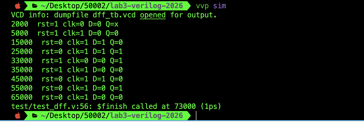
The output of the testbench should be as follows:
The output waveform is as follows:
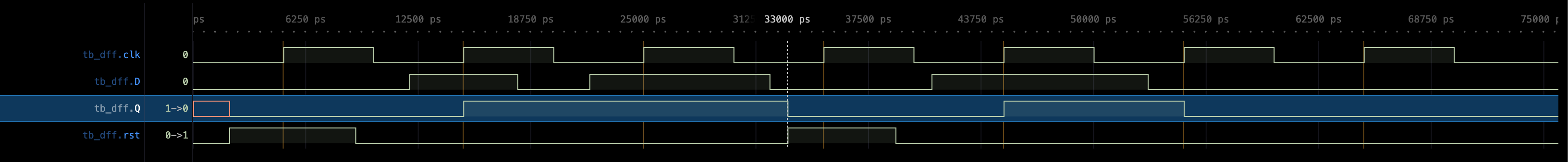
Things to observe:
Q’s value is synchronised with the rising clock edge- Changes in
Dvalues in-between rising clock edges are ignored - Reset happens asynchronously and takes precedence. At around 33000 ps mark,
Qchanges to0immediately as soon as reset is1, regardless of theclk.
dff with reset and en
When you add an en to the dff, we have one more case to test: whether Q changes with D at rising clock edges if en is 0. Everything else remains the same.
The following testbench produces relevant waveforms:
`timescale 1ns/1ps

module tb_dff_en;

  reg  clk;
  reg  D;
  reg  en;
  reg  rst;
  wire Q;

  // DUT
  dff_en dut (
    .D(D),
    .clk(clk),
    .rst(rst),
    .en(en),
    .Q(Q)
  );

  // ANSWER KEY, hardcoded
  reg expected_Q [0:13];

  initial begin
    expected_Q[0] = 1'b0; // rst = 1
    expected_Q[1] = 1'b1; // D = 1, en = 1, rst = 0
    expected_Q[2] = 1'b1; // D = 0, en = 0, rst = 0, maintain prev value
    expected_Q[3] = 1'b1; // D = 1, en = 1, rst = 0
    expected_Q[4] = 1'b1; // D = 0, en = 0, rst = 0, maintain prev value
    expected_Q[5] = 1'b0; // rst = 1
    expected_Q[6] = 1'b1; // D = 1, en = 1, rst = 0
    expected_Q[7] = 1'b1; // D toggles exactly at posedge but en 0, maintain prev value
    expected_Q[8] = 1'b0; // D = 0, en = 1, rst = 0
    expected_Q[9] = 1'b0; // D = 1, en = 0, rst = 0, maintain prev value
    expected_Q[10] = 1'b0; // rst = 1
    expected_Q[11] = 1'bx; // D toggles exactly at posedge and en is 1, so unexpected
    expected_Q[12] = 1'bx; // en = 0, so maintains prev value
    expected_Q[13] = 1'bx; // en = 0, so maintains previous value
  end

  // Clock: 10 ns period
  initial begin
    clk = 0;
    forever #5 clk = ~clk;
  end

  // Waveform
  initial begin
    $dumpfile("tb_dff_en.vcd");
    $dumpvars(0, tb_dff_en);
    $dumpvars(0, dut); // includes next_Q
  end


  // -------------------------------------------------
  // Checker: compare after each rising edge
  // -------------------------------------------------
  integer checker_index;
  initial checker_index = 0;

  always @(posedge clk) begin
    #1; // sample slightly after rising edge
    if (checker_index < 14) begin
      if (expected_Q[checker_index] !== 1'bx) begin
        if (Q !== expected_Q[checker_index]) begin
          $display(
            "FAIL at edge %0d : Q=%b expected=%b",
            checker_index, Q, expected_Q[checker_index]
          );
          $finish;
        end
      end
    end
    checker_index = checker_index + 1;
  end


  integer cycle;
  initial begin
    D   = 0;
    en  = 0;
    rst = 0;

    // Initial async reset
    #3 rst = 1;
    #4 rst = 0;

    for (cycle = 0; cycle < 10; cycle = cycle + 1) begin
      @(negedge clk);

      // Far before next posedge
      #1  D  = ~D;

      // Just before posedge
      #3  en = ~en;

      // Occassionally change D exactly at posedge time
      if (cycle == 5 || cycle == 8) begin
        // Exactly at posedge time
        #1  D  = ~D;
      end
      else #1

      // Just after posedge toggle only on some cycles
      if (cycle == 2 || cycle == 3 || cycle == 9) begin
      #1  D  = ~D;
      end
      else #1

      // Mid-cycle change, but only at some cycles
      if (cycle == 5)
        #2  en = ~en;

      // Occasionally assert async reset mid-cycle
      if (cycle == 3 || cycle == 7 || cycle == 9) begin
        #1 rst = 1;
        #5 rst = 0;
      end
    end

    #5;
    $display("PASS");
    $finish;
  end

endmodule
You should arrive at the following waveform:
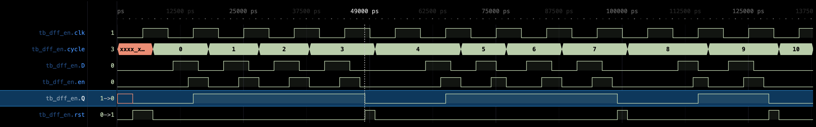
Things to lookout for:
- If
enis 0,Qmaintains its old value, but ifenis1, then it behaves like a regulardff Q’s changes is synchronised to the rising edge of the clock except when reset is1- At around 49000 ps,
Qbecomes0because reset is1, even thoughenis 0 and it’s in-between rising clock edges
Using AI to produce testbenches for you
Writing a long testbench can be quite taxing, and repetitive. It is very tempting to just ask AI to spit out some for you, and in fact, that is the right move especially with well known language like Verilog. However, it is very important that you are specific when prompting AI to generate a testbench for you.
You need to define all edge cases as much as possible, and also forces it to provide an answer key.
A complete prompt like the following should be good enough:
Write a plain 2005 Verilog testbench for a D flip-flop with asynchronous active-high reset and enable. The testbench should run for many clock cycles and continuously exercise the design rather than using a few hand-picked cases. The clock period is 10 ns. Across the run, the input D must change at different times relative to each rising clock edge: well before the edge, just before the edge, exactly at the same simulation time as the edge, and after the edge, so the waveform clearly shows how sampling works and that changes at the edge itself are undefined. The enable signal should toggle between 0 and 1 multiple times; when enable is 1 and reset is 0, Q should follow D at rising edges, and when enable is 0 and reset is 0, Q should hold its previous value even though D continues to change. The reset signal must be asserted asynchronously at times not aligned with the clock and must override everything else: whenever reset is 1, Q must immediately go to 0 regardless of enable or D. The testbench must include a simple reference model updated on posedge clk or posedge reset that acts as an answer key for defined behavior, and the reference values should be visible in the waveform for comparison rather than used for strict pass-fail checking. The testbench should dump a VCD waveform.
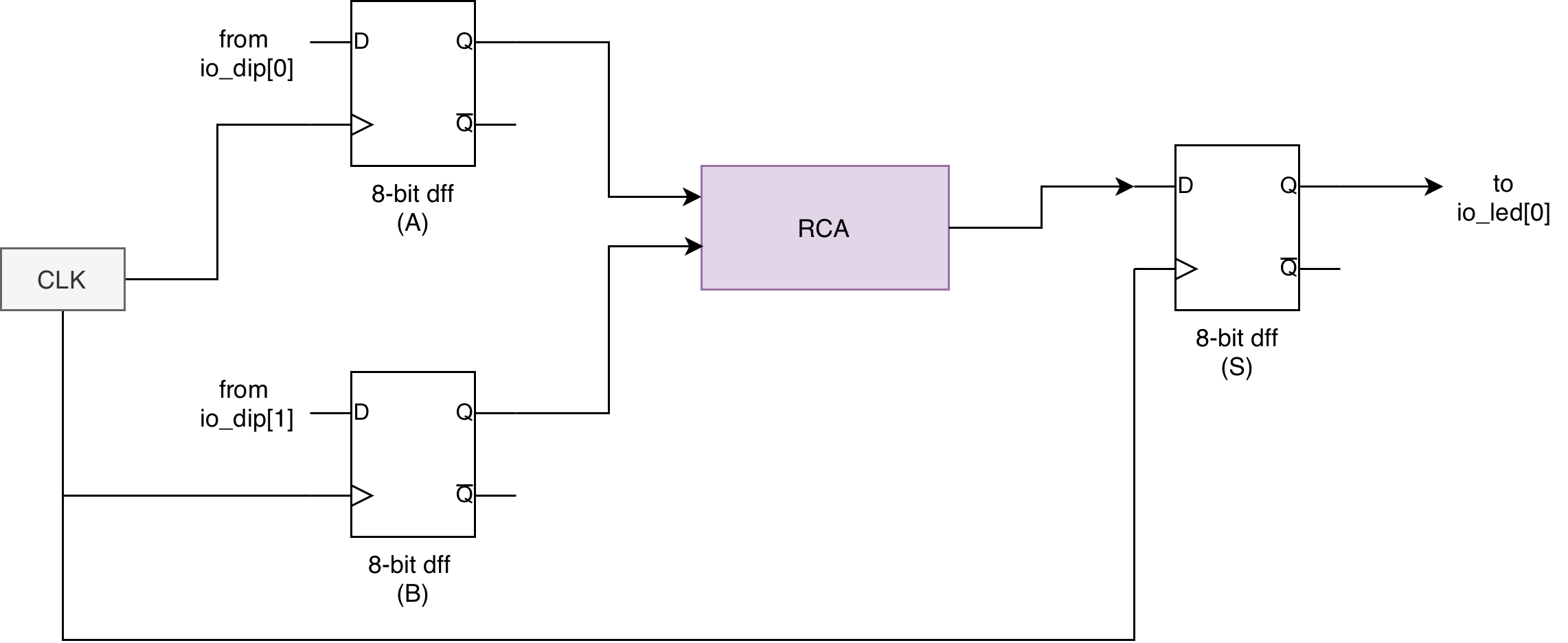
Creating a Pipeline
A pipeline means splitting a computation into multiple stages separated by registers, so different inputs can be processed at the same time, one stage per clock cycle. Each clock edge, the stage registers capture intermediate results and pass them to the next stage, which increases throughput (more results per second) even if the total latency per item becomes multiple cycles.
Simple Registered Adder
To demonstrate this pipeline concept, we will create a pipelined rca (created from the previous lab) so that data can be fed to it in a time-ordered sequence.
Recall: Register
In digital design, a register is a storage element built from flip-flops.
- A 1-bit register is essentially one D flip-flop (stores 1 bit).
- An N-bit register is N flip-flops in parallel sharing the same clock (stores an N-bit value, like 32 bits).
Registers are used to hold state: CPU registers, pipeline registers, FSM state registers, counters, etc. They update on clock edges (often with optional reset and enable) and stay stable between edges.
// Pipelined Ripple-Carry Adder
// Registers: a_reg, b_reg, s_reg
// Latency: 2 cycles (inputs registered on cycle N, sum registered on cycle N+1)
module pipelined_rca #(
    parameter SIZE = 8
)(
    input                  clk,
    input                  rst,     // async active-high reset
    input                  en,      // pipeline enable (stalls all regs when 0)
    input  [SIZE-1:0]      a,
    input  [SIZE-1:0]      b,
    input                  ci,
    output [SIZE-1:0]      s,
    output                 co       // optional
);

    // Stage 0 registers (registered inputs)
    wire [SIZE-1:0] a_q;
    wire [SIZE-1:0] b_q;

    genvar i;

    generate
        for (i = 0; i < SIZE; i = i + 1) begin : in_regs
            dff_en u_a_reg (.D(a[i]), .clk(clk), .rst(rst), .en(en), .Q(a_q[i]));
            dff_en u_b_reg (.D(b[i]), .clk(clk), .rst(rst), .en(en), .Q(b_q[i]));
        end
    endgenerate

    // Combinational adder between stages
    wire [SIZE-1:0] sum_comb;
    wire            co_comb;

    rca #(.SIZE(SIZE)) u_rca (
        .a(a_q),
        .b(b_q),
        .ci(ci),
        .s(sum_comb),
        .co(co_comb)
    );

    // Stage 1 registers (registered sum)
    wire [SIZE-1:0] s_q;
    wire co_q;

    generate
        for (i = 0; i < SIZE; i = i + 1) begin : out_regs
            dff_en u_s_reg (.D(sum_comb[i]), .clk(clk), .rst(rst), .en(en), .Q(s_q[i]));
        end
    endgenerate

    dff_en u_co_reg (.D(co_comb), .clk(clk), .rst(rst), .en(en), .Q(co_q));

    assign s  = s_q;
    assign co = co_q;

endmodule
Note how we never use instance.output_port here and always use intermediary wire instead.
The Benefit of Utilising the dff Module
At this point, it is important to be explicit about where sequential behavior lives in this design.
In the registered adder above, ALL state and all clocked behavior are fully encapsulated inside the dff_en or dff modules. Each dff instance is a concrete D flip-flop with an enable and reset. As a result the parent module pipelined_rca contains no clocked always blocks
- There are no
always @(posedge clk)blocks - There are no nonblocking assignments (
<=) anywhere in this module
This is intentional and correct.
Once a design instantiates explicit flip-flops like the dff/dff_end modules, the surrounding logic must be treated as purely combinational datapath wiring. The timing semantics are already defined by the flip-flop boundaries.
We handle clocking discipline structurally, with clear separation on where the sequential behavior lives, which is only within the dff modules. The bigger modules that utilises these dffs describes a datapath composed of these arrays of dffs (registers) and combinational logic between them (the rca).
This mirrors how real hardware is reasoned about at the block-diagram level, and is intentionally taught to you this way to be more closely aligned with the lecture materials and basic understanding of circuitry. In LucidV2, this is the approach as well.
Why no nonblocking assignments are needed when you use dff module
Nonblocking assignments exist to correctly describe edge-triggered state updates inside a clocked procedural block. Their role is to ensure that ALL registers sample old values and update simultaneously at a clock edge.
In this design:
- The
dff_enmodule already implements that behavior internally - Each
dff_enhas its ownalways @(posedge clk)with nonblocking assignment - The parent module never updates state directly
Therefore, adding another always @(posedge clk) in pipelined_rca would be both redundant and conceptually incorrect. It would blur the separation between state elements (the dffs holding a series of a, b, s and cout values over time) and combinational datapath (the RCA), which is precisely what this lab aims to make clear.
What if we did not use a dff module and let Verilog infer registers?
An alternative implementation would be to remove the dff_en modules entirely and write something like this to create a pipelined/registered adder:
This is the style most AI tools (and many experienced RTL designers) will produce if you ask for a “clocked/pipelined/registered adder” directly. It is functionally correct, but it is not beginner-friendly because it collapses several concepts into one place. To understand why it works, you already need to know:
- How registers are inferred from
always @(posedge clk ...)blocks (and what makes something a flip-flop vs “just logic”)- Why nonblocking (
<=) is required in clocked sequential logic, and what can break if you use blocking (=)- How pipelining is expressed as “stage 0 regs” feeding combinational logic feeding “stage 1 regs”
- Why enables must hold state (and what a stall means across multiple pipeline stages)
- Why separating sequential vs combinational logic matters for readable control-datapath design
For beginners, this style hides the central lesson, which is that: a *pipeline is registers PLUS combinational logic between them*. When you use an explicit
dff/dff_enmodule, the pipeline boundaries become visually obvious, and you can focus on timing and data movement without simultaneously learning register inference rules and assignment semantics.
// Pipelined Ripple-Carry Adder (inferred registers version)
// Registers inferred: a_q, b_q, ci_q, s_q, co_q
// Latency: 2 cycles
//   - cycle N:     input regs capture a,b,ci
//   - cycle N+1:   output regs capture sum/co computed from registered inputs
//
// Notes:
// - Uses nonblocking assignments in clocked blocks (required for correct sequential semantics).
// - en stalls the entire pipeline when 0 (all regs hold their values).
module pipelined_rca_inferred #(
    parameter integer SIZE = 8
)(
    input  wire                 clk,
    input  wire                 rst,     // async active-high reset
    input  wire                 en,      // pipeline enable (stall when 0)
    input  wire [SIZE-1:0]       a,
    input  wire [SIZE-1:0]       b,
    input  wire                 ci,
    output wire [SIZE-1:0]       s,
    output wire                 co
);

    // Stage 0 registers (registered inputs)
    reg  [SIZE-1:0] a_q;
    reg  [SIZE-1:0] b_q;
    reg             ci_q;

    // Combinational adder between stages (driven by stage-0 regs)
    wire [SIZE-1:0] sum_comb;
    wire            co_comb;

    rca #(.SIZE(SIZE)) u_rca (
        .a (a_q),
        .b (b_q),
        .ci(ci_q),
        .s (sum_comb),
        .co(co_comb)
    );

    // Stage 1 registers (registered outputs)
    reg  [SIZE-1:0] s_q;
    reg             co_q;

    // Stage 0: capture inputs
    always @(posedge clk or posedge rst) begin
        if (rst) begin
            a_q  <= {SIZE{1'b0}};
            b_q  <= {SIZE{1'b0}};
            ci_q <= 1'b0;
        end else if (en) begin
            a_q  <= a;
            b_q  <= b;
            ci_q <= ci;
        end
        // else: hold state (stall)
    end

    // Stage 1: capture adder outputs
    always @(posedge clk or posedge rst) begin
        if (rst) begin
            s_q  <= {SIZE{1'b0}};
            co_q <= 1'b0;
        end else if (en) begin
            s_q  <= sum_comb;
            co_q <= co_comb;
        end
        // else: hold state (stall)
    end

    assign s  = s_q;
    assign co = co_q;

endmodule
In the implementation above, inference happens:
- Verilog infers registers based on the clocked
alwaysblock - The registers still exist in hardware, just like the approach that utilises
dffmodules separately
Therefore, the synthesis result can be functionally equivalent, but it is definitely harder to visually identify pipeline stages for beginners, and obscures where registers conceptually sit in the datapath. It mixes state, control, and datapath logic which is probably okay for experts to use and save time with concise code, but is definitely not recommended for absolute beginners in RTL.
Connection to control, datapath, and FSMs
This registered adder is a minimal example of a datapath, which is the main topic of the next lab:
- Registers hold values across cycles
- Combinational logic transforms those values
- Data moves forward on clock edges
In the upcoming control-datapath and FSM lab:
- The datapath will contain registers similar to
a_q,b_q, ands_q - An FSM will generate control signals such as enables, selects, and resets
- The FSM itself will be implemented using registers to store states, often via the same
dffabstraction
We hope that by separating flip-flops into explicit modules now, you build the correct habit and realise that: datapath logic is combinational, state lives in registers (array of dff), control decides WHEN registers update, clocking is never implicit or scattered.
Testbench Design
In this section, we outline some tips and learning points so that you can write your own testbench to ensure the correctness of your pipelined_rca.
A registered (pipelined) adder like the above does not produce the sum in the same cycle the inputs are applied. If the DUT has 2 pipeline stages, then:
- Inputs applied in cycle
ishould appear at outputs in cyclei+2 - The testbench must delay the expected answer by 2 clocks before comparing
The testbench for the registered adder is not a trivial one, and although it is tempting to just ask an AI to create one for you, it is important to keep a few steps in mind. Below are the general approaches for testbench design.
Decide what is “procedural state” vs “driven by hardware”
At the beginning of your testbench, you should decide signal types based on who drives it:
- Driven by the testbench in procedural blocks (
initial,always) Usereg(Verilog) Examples:clk,rst,en,a,b,ci, plus internal testbench holding variables. - Driven by the DUT (module outputs)
Use
wireExamples:s,co.
Recap
Arrays of vectors in plain Verilog are typically
reg [W-1:0] name [0:N-1].
Parameterize the testbench so it matches multiple DUT sizes
You should define stuffs like:
lcalparam SIZE = ...;(bit width)localparam N = ...;(number of test vectors)
Then apply it consistently throughout your testbench like so to make a bulk of your code reusable.
reg [SIZE-1:0] a, b;wire [SIZE-1:0] s;- arrays sized by
N
Precompute vectors as an answer key
You would need to be very conscious about the values you are testing. You need to ensure that they are correct and are comprehensive:
- Create input tables:
a_vec[i],b_vec[i],ci_vec[i] - Create output tables:
s_exp[i],co_exp[i]
In Verilog, this is often done in an initial begin ... end that assigns each entry explicitly, because standard Verilog does not have fancy literals or dynamic array helpers like you saw in Lucid const.
Create pipelined delay registers for the answer values
This is useful for any DUT with pipelined system. Since there are two registers in the pipelined adder, you need to pass the answer key through the same number registers as well. In this particualr case, you can make a tiny shift register system:
- stage 1:
s_exp_q1,co_exp_q1 - stage 2:
s_exp_q2,co_exp_q2 q2gets its input from the output ofq1
Then the comparison of the pipelined adder’s output is against *_q2.
To be clear, you need to do the following:
- at cycle i you load
*_nowfrom table entry i - on posedge,
*_nowis captured into q1, and q1 into q2 (when enabled) - at cycle i, you compare DUT output against q2, which corresponds to input from i-2
Pay attention to any en signals and async reset used in DUT
If DUT pipeline registers update only when en==1, then the expected pipeline must also shift only when en==1. If DUT has async reset, expected pipeline should reset the same way.
We need to build an always @(posedge clk or posedge rst) for the pipelined answer key that mirrors DUT control:
- on reset: clear q1/q2
- else if enabled: shift q1/q2
Recap
Nonblocking assignments (
<=) should be used to build these 2-stage shift register. Note that the order of nonblocking assignments does not create sequential dependency (it models parallel FF updates)
Clock generation and negedge
You should be very clear that:
- DUT captures inputs on
posedge - Therefore testbench should change inputs on
negedge(half-cycle earlier) so they are stable before the capture edge
For each test value:
- wait for
@(negedge clk) - drive
a,b,ci, and*_now - wait for
@(posedge clk)to let DUT capture - then (after sufficient fill cycles) compare outputs
While it is tempting to use #1 delays for “stability” before checking the result like you have tried before during the making of combinational-logic test benches, event control on clock edges is the clean approach.
Pipeline fill and drain
Because latency is 2 cycles:
- the first 2 cycles after you start streaming vectors do not have valid DUT outputs for comparison
- after feeding the last real vector, you still need 2 extra cycles (“flush”) to observe the final results
So the main testbench typically runs N + latency iterations.
You are recommended to express latency as a parameter too, even though you know its value is 2 for this lab:
localparam LAT = 2;- loop to
N + LAT
Compare with case inequality and count errors
When comparing DUT’s output (s and cout) against the *.q2 (output of the answer key’s 2-stage pipeline register), you should:
- Use
!==(case inequality), not!=Because if the DUT outputs X due to uninitialized regs,!=can behave in surprising ways.!==treats X as a real value and will flag mismatch. - Maintain an
errorscounter and print details on failure:- cycle index
- got vs expected
- maybe also print the corresponding input vector (useful for debugging)
Use proper formatted strings during prints:
%0dfor integers%02hfor 8-bit hex with leading zero
Reset sequencing and enabling
Any DUT should be reset in the beginning, before you feed the first test vector.
If you use async reset (which is the case here), you can pulse rst without the clock, but still you must ensure you release reset cleanly before starting comparisons.
- Keep
enasserted at all times if the goal is basic functionality, and that you’re already sure that yourdff_enunit used inpipelined_rcais already heavily tested and corect - If you want a stronger test, include a few cycles where
en=0and confirm outputs “stall” and your expected pipeline also stalls.
Sample Waveform Output
You should create sufficient test cases, e.g: 16 at least and confirm on the waveform that your adder is giving the expected output:
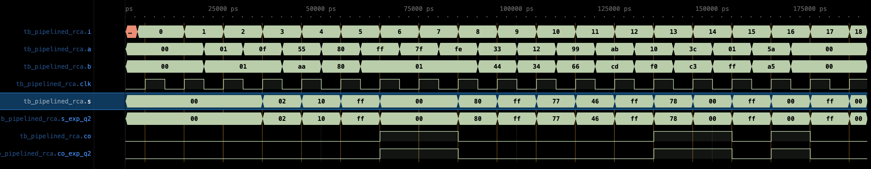
Summary Approach
When writing any testbench, consider these important steps:
- Identify which signals TB drives (
reg) vs DUT drives (wire). - Decide widths and counts with
localparam. - Build vector tables for inputs and expected outputs.
- Introduce
*_nowas “expected for the vector I am currently applying.” - Implement an expected shift register of depth equal to DUT latency, gated by
en, reset byrst. - Drive inputs and
*_nowon negedge. - On posedge, after the fill period, compare DUT outputs to the delayed expected (
q2). - Run
N + latencycycles so the last vectors have time to emerge. - Count errors, print concise failure lines, then print pass/fail summary.
Refer to the appendix for useful Verilog syntaxes to build this testbench.
Frequency Divider
In simulation testbenches, you normally do not need a frequency divider because you can directly choose a slower clk period (or insert #delay in stimulus). On FPGA hardware, the board clock is very fast (100 MHz clk on our Alchitry board), so “human-speed” behaviors like LED blinking, button-driven stepping, or visibly slow FSM progress require generating a slower tick.
There are two common divider styles.
Bit-tap counter divider (recommended)
Here’s the general steps:
- Implement a free-running counter clocked by the main
clk. - Use one counter bit as
slow_clk, e.g.slow_clk = cnt[STAGES-1]. - This keeps the design in a single clock domain (everything is synchronous to the original
clk). - Best practice is often to use the slow signal as a clock-enable pulse (tick) rather than as a real clock, so the whole design still uses only the main
clk.
The suggested implementation is as follows:
When STAGES = N, we are producing a clock with 1/2^n the frequency of the original clk.
module slowclock_tap #(
    parameter integer STAGES = 27
)(
    input  wire clk,
    input  wire rst,      // async active-high reset
    output wire slow_clk
);

  localparam integer STAGES_I = (STAGES < 1) ? 1 : STAGES;

  reg [STAGES_I-1:0] cnt;

  always @(posedge clk or posedge rst) begin
    if (rst) cnt <= {STAGES_I{1'b0}};
    else     cnt <= cnt + 1'b1;
  end

  // Bit tap: divides clock by 2^STAGES (full period in clk cycles)
  // Toggles every 2^(STAGES-1) cycles.
  assign slow_clk = cnt[STAGES_I-1];

endmodule
You can use it with the following testbench:
`timescale 1ns/1ps

module tb_slowclock_tap;

  // Make it small so you can see toggles quickly
  localparam integer STAGES = 4;

  reg  clk;
  reg  rst;
  wire slow_clk;

  // DUT
  slowclock_tap #(.STAGES(STAGES)) dut (
    .clk(clk),
    .rst(rst),
    .slow_clk(slow_clk)
  );

  // 10 ns period clock
  initial begin
    clk = 1'b0;
    forever #5 clk = ~clk;
  end

  // Dump waves
  initial begin
    $dumpfile("tb_slowclock_tap.vcd");
    $dumpvars(0, tb_slowclock_tap);
    $dumpvars(0, dut);
  end

  initial begin
    rst = 1'b1;
    #17;          // deassert off-edge to make it obvious in waveform
    rst = 1'b0;

    // Run long enough to see several slow_clk transitions
    #500;
    $finish;
  end

endmodule
Ripple divider
This method generates a slow clock using a chain of dffs:
- Each flip-flop is clocked by the output of the previous stage.
- Functionally, it also divides frequency, and the last stage toggles slowly.
However, it creates multiple derived clocks (many clock domains) and the transitions are not aligned to the main clock, so it is generally not preferred for larger designs on FPGA.
Here’s a suggested implementation for educational purposes:
When STAGES = N, we are producing a clock with 1/2^n the frequency of the original clk.
module clk_divider #(
    parameter integer STAGES = 27
)(
    input  wire clk,
    input  wire rst,
    output wire slow_clk
);

localparam integer STAGES_I = (STAGES < 1) ? 1 : STAGES;

wire [STAGES_I-1:0] din;
wire [STAGES_I-1:0] clkdiv;

dff d0 (.clk(clk), .rst(rst), .D(din[0]), .Q(clkdiv[0]));

genvar i;
generate
  for (i = 1; i < STAGES_I; i = i + 1) begin : dff_gen
    dff di (.clk(clkdiv[i-1]), .rst(rst), .D(din[i]), .Q(clkdiv[i]));
  end
endgenerate

assign din = ~clkdiv;
assign slow_clk = clkdiv[STAGES_I-1];

endmodule
You can use the following testbench:
`timescale 1ns / 1ps

module tb;

  localparam integer STAGES = 3;

  reg  clk;
  reg  rst;
  wire slow_clk;

  clk_divider #(.STAGES(STAGES)) uut (
    .clk(clk),
    .rst(rst),
    .slow_clk(slow_clk)
  );

  always #5 clk = ~clk; // 100 MHz clock

  initial begin
    // VCD waveform dump
    $dumpfile("tb_clk_divider.vcd");
    $dumpvars(0, tb);   // dump everything under tb (includes uut)

    clk = 0;
    rst = 1;

    #10 rst = 0;

    #500;
    $finish;
  end

endmodule
Are they functionally the same?
At a high level, yes: both produce a slower square wave by repeatedly dividing by 2 per stage. The waveform will look similar, something like this for STAGES = 3:

But electrically and for “clean synchronous design,” they are not equivalent:
- The bit-tap counter produces a slow signal derived from logic clocked by
clkonly. - The ripple divider uses intermediate signals as clocks, which can introduce clock skew and domain-crossing issues if you use those clocks to drive other logic.
For 50.002 projects, either can be used to slow down visible hardware behavior, but the counter bit-tap approach is the safer default in Verilog FPGA work.
Conclusion
In this lab, we moved from thinking about logic as static wiring to thinking about systems that evolve one clock edge at a time. We saw how memory is introduced deliberately through edge-triggered flip-flops, why missing assignments mean very different things in combinational versus clocked blocks, and how enable and reset signals interact with flip-flops.
By building and testing a pipelined adder, we also encountered a key systems concept: latency. Registers impose delay, but they give us synchronization, predictability, and the ability to scale designs cleanly. Once a design is pipelined, correctness is no longer about “what is the output right now,” but about which cycle an output corresponds to. Your testbench must reflect that same timing discipline.
Here are the key learning points from this lab that reinforces understanding of lecture materials:
- Clock edges define truth.
- Anything that happens between edges is transient and intentionally ignored by synchronous systems. Changes exactly at the edge are not reliable, in simulation or in real hardware.
- Good testbenches mirror hardware thinking.
- We shall not “check immediately.” We need to align stimulus to edges, delay expectations by pipeline latency, and compare only when the design promises valid data.
These ideas form the foundation for finite state machines, pipelines, and eventually CPUs which we will discover in the later weeks. If combinational logic answers the question “what should the output be,” clocked design answers the more important one: when should that answer be trusted.
Appendix
Useful Verilog Syntax
Below contains a list of useful Verilog syntaxes to write this registered adder testbench.
timescale 1ns/1ps:
- Defines the simulation time unit and time precision.
- Example:
#5means 5 ns when the time unit is 1 ns. - Precision (1 ps) affects rounding of delays, not functional logic.
- You do not need to memorize this, but you must know it affects all
#delays.
Module instantiation with parameters:
- Syntax:
dut #(.SIZE(SIZE)) (...)
- The left
SIZEis the DUT’s parameter name. - The right
SIZEis a constant defined in the testbench. - This allows the same DUT to be tested at different bit widths.
Arrays of vectors (memory-like tables):
- Syntax:
reg [SIZE-1:0] a_vec [0:N-1];
- Rightmost index is the array index.
- Each entry is a
SIZE-bit vector. - Commonly used for precomputed input vectors and expected outputs.
Event controls:
- Syntax:
@(negedge clk)@(posedge clk)
- These are synchronization points, not delays.
- Used to align testbench actions with clock edges.
- Typical pattern:
- Drive inputs on
negedge. - Let DUT capture on
posedge.
- Drive inputs on
Nonblocking assignments in sequential blocks:
- Use
<=inside clockedalwaysblocks. - Models flip-flop behavior correctly.
- All right-hand sides are evaluated before any left-hand side updates.
- Order of
<=statements does not imply execution order.
Blocking vs nonblocking in the testbench:
- Blocking assignment
=:- Suitable in
initialblocks that describe procedural flow. - Executes in order, top to bottom.
- Suitable in
- Nonblocking assignment
<=:- Required in clocked logic, including golden pipeline registers.
- Matches hardware timing behavior.
Waveform dumping (Icarus / GTKWave):
- Common system tasks:
$dumpfile("wave.vcd");$dumpvars(0, tb_name);
- Enables viewing internal signals in a waveform viewer.
- Simulator-specific but extremely useful for debugging.
Loop index declaration:
- Syntax:
integer i;
- Commonly used for
forloops in testbenches. - Automatically treated as a signed integer.
- Suitable for indexing vector tables and counting cycles.