 50.002 CS
- CMOS Circuit Boolean Expression (Basic)
- Combinational Circuit’s Functional Specs (Basic)
- Simple Boolean Algebra (Basic)
- Reading ROM (Basic)
- Implementing Half-Adder using ROM (Basic)
- CMOS Gate Analysis (Basic)
- Simplifying a Rather Complicated Boolean Expression (Intermediate)
- CMOS Gate Design (Challenging)
- Another Boolean Minimisation (Basic)
- Reading Karnaugh’s Map (Basic)
- The FPGA (Challenging)
50.002 Computation Structures
Information Systems Technology and Design
Singapore University of Technology and Design
Logic Synthesis
Each topic’s questions are grouped into three categories: basic, intermediate, and challenging. You are recommended to do all basic problem set before advancing further.
CMOS Circuit Boolean Expression (Basic)
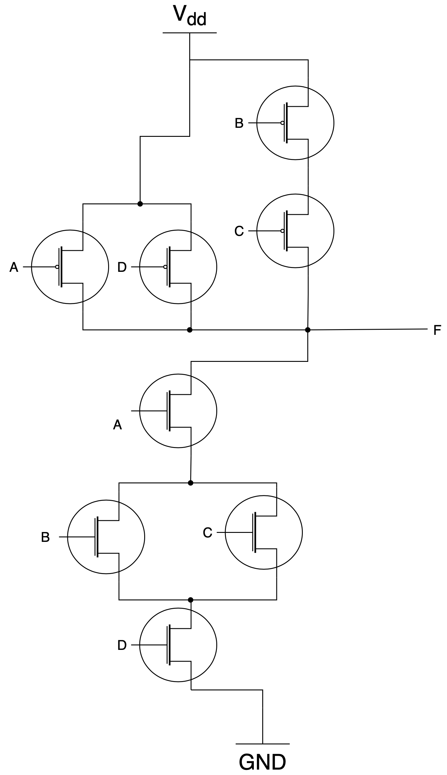
- Draw the truth table of the CMOS circuit above.
- What is the boolean expression for the CMOS circuit shown?
1. The truth table of the CMOS circuit contains 16 lines since there are 16 possible input combinations and 1 possible output bit:
$$\begin{matrix}
A & B & C & D & F \\ \hline 0 & 0 & 0 & 0 & 1 \\ 0 & 0 & 0 & 1 & 1 \\ 0 & 0 & 1 & 0 & 1 \\ 0 & 0 & 1 & 1 & 1 \\ 0 & 1 & 0 & 0 & 1 \\ 0 & 1 & 0 & 1 & 1 \\ 0 & 1 & 1 & 0 & 1 \\ 0 & 1 & 1 & 1 & 1 \\ 1 & 0 & 0 & 0 & 1 \\ 1 & 0 & 0 & 1 & 1 \\ 1 & 0 & 1 & 0 & 1 \\ 1 & 0 & 1 & 1 & 0 \\ 1 & 1 & 0 & 0 & 1 \\ 1 & 1 & 0 & 1 & 0 \\ 1 & 1 & 1 & 0 & 1 \\ 1 & 1 & 1 & 1 & 0 \\ \hline \end{matrix}$$
1. The final boolean expression is: $$F = \overline{A(B+C)D}$$ This is obtained straight from the diagram. Look at the **pull down** circuitry and you will figure out that if A *and*, B *or* C, *and* D is 1, then you will get a `0` as the output, hence the expression. Ideally you don't take the sum of products for this case because there are so many `1`s. You can look at rows with `0` instead, do the sum of products for that and NOT the entire term. You will need a few steps to simplify it: $$
\begin{align}
F &= \overline{A\bar{B}CD + AB\bar{C}D + ABCD} \\
&= \overline{AD(\bar{B}C + B\bar{C} + BC)}\\
&= \overline{AD(C(\bar{B}+B)+ B\bar{C})}\\
&= \overline{AD(C+B\bar{C})}\\
&= \overline{AD(C+B)}\\
&= \overline{A(B+C)D}
\end{align}
$$
Combinational Circuit’s Functional Specs (Basic)
Consider the following circuit that implements the 2-input function \(H(A,B)\):
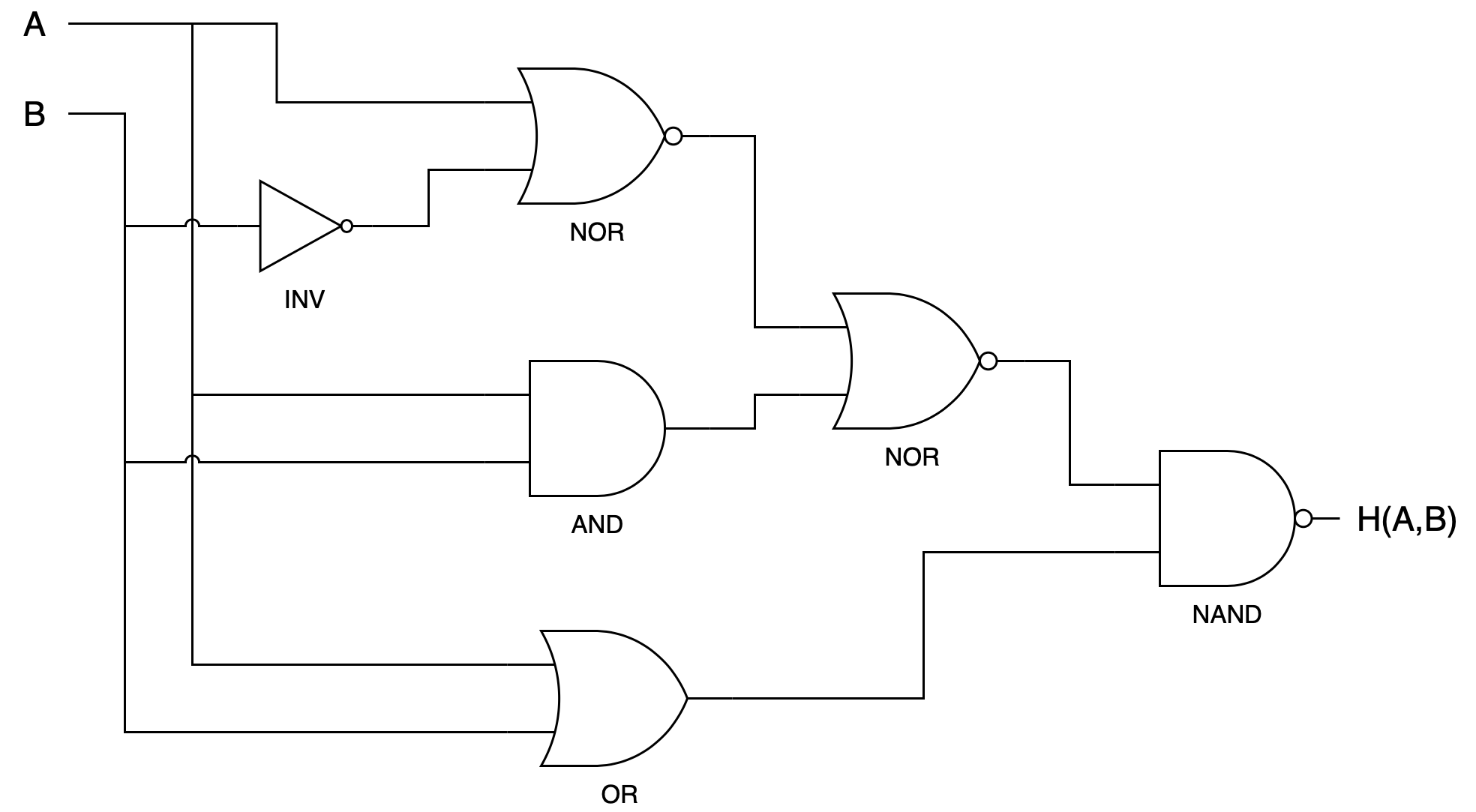
- Write down the truth table for \(H\).
- Give a sum-of-products expression that corresponds to your truth table.
- Using the information below, what are the tcd and tpd of the circuit?
- tcd and tpd of
NOR2: 5ns, 30ns - tcd and tpd of
NAND2: 5ns, 30ns - tcd and tpd of
AND2: 6ns, 50ns - tcd and tpd of
OR2: 10ns, 20ns - tcd and tpd of
INV: 1ns, 3ns
- tcd and tpd of
- The truth table for H is as follows: $$\begin{matrix} A & B & H \\ \hline 0 & 0 & 1\\ 0 & 1 & 1 \\ 1 & 0 & 0 \\ 1 & 1 & 1\\ \hline \end{matrix} $$
- We begin by finding the expression of the topmost two circuits and applying de Morgan's law: $$\overline{A + \overline{B}} = \overline{A}B$$
Then, we find the expression of the next pair, which is: $$AB$$ We combine this with the above using a NOR gate and reduce the result, $$\overline{\overline{A}B + AB} = \overline{B}$$
Finally, we find the expression for the bottom two pairs, which is simply: $$A+B$$ Combining this with the above expression, we reduce and apply de Morgan's law: $$\begin{aligned} \overline{(A+B)\overline{B}} &= \overline{A \overline{B} + B \overline{B}} = \overline{A\overline{B}} = \overline{A} + B\\ \end{aligned}$$ - The **contamination** delay is the path (from any input to any output) that results in the **shortest** time: `NOR2` + `NOR2` + `NAND2` = 5 + 5 + 5 = 15ns. The **propagation** delay is the path (from any input to any output) that results in the **longest** time: `AND2` + `NOR2` + `NAND2` = 50 + 30 + 30 = 110ns.
Simple Boolean Algebra (Basic)
Given the following truth table,
\[\begin{matrix} A & B & C & OUT \\ \hline 0 & 0 & 0 & 1 \\ 0 & 0 & 1 & 1 \\ 0 & 1 & 0 & 1 \\ 0 & 1 & 1 & 0 \\ 1 & 0 & 0 & 1 \\ 1 & 0 & 1 & 1 \\ 1 & 1 & 0 & 1 \\ 1 & 1 & 1 & 0 \\ \hline \end{matrix}\]Choose all correct Boolean expression(s) of this circuit:
(a). \(OUT = \bar{C} + \bar{B}\)
(b). \(OUT = \bar{A} \cdot \bar{B} + A \cdot \bar{B} + B \cdot \bar{C}\)
(c). \(OUT = \bar{A} \cdot \bar{C} + A \cdot B \cdot \bar{C} + \bar{B}\)
(d). \(OUT = \bar{A} \cdot B + A \cdot B \cdot \bar{C} + \bar{B}\)
Hint
Express the table in terms of sum of products first and then simplify the expression.
(a), (b), and (c) are all equivalent and represents the truth table.
Reading ROM (Basic)
What is the the sum-of-products for the following ROM (Read Only Memory)?
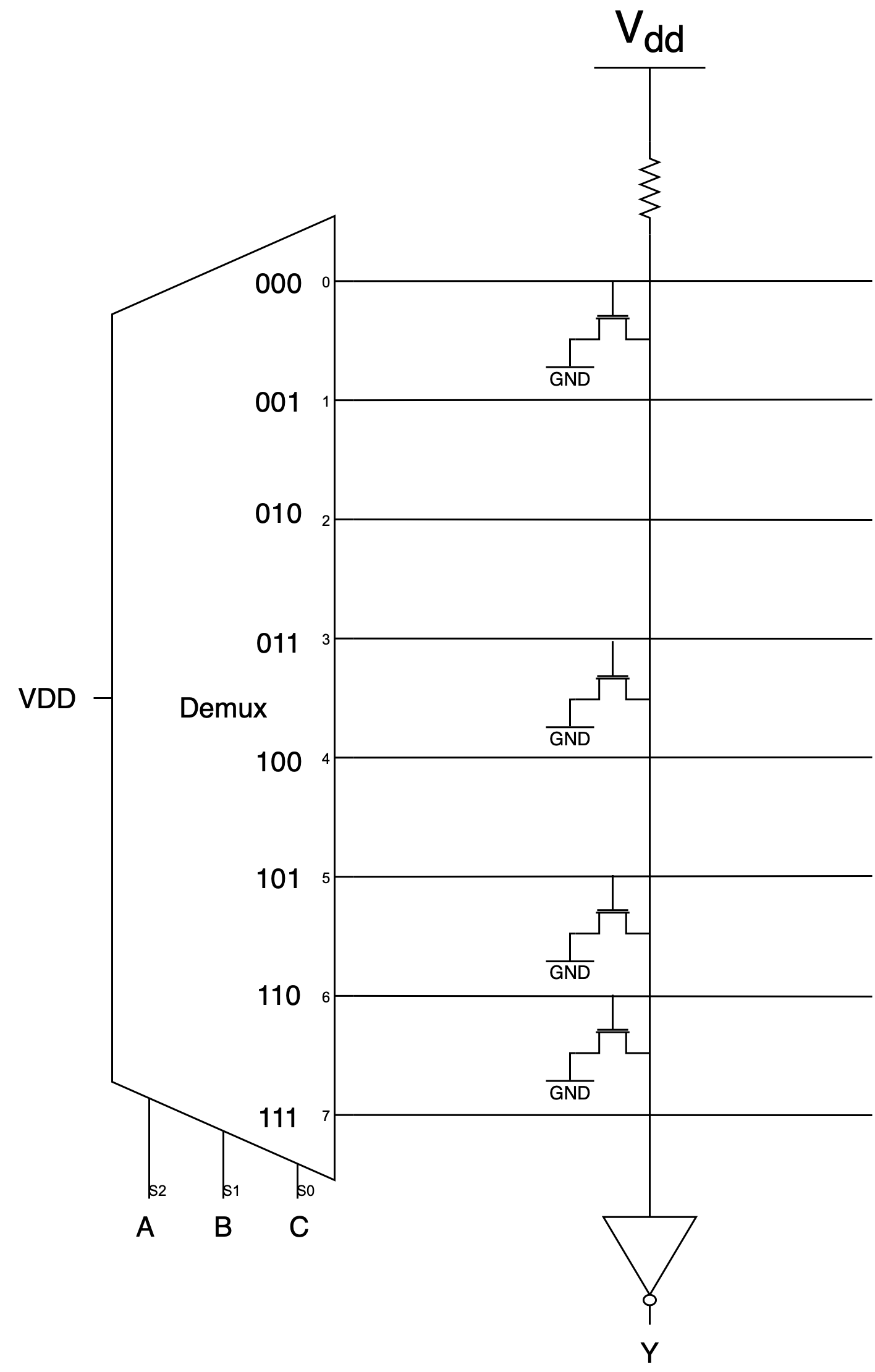
$$Y = \bar{A}\bar{B}\bar{C} + \bar{A}BC + A \bar{B} C+ AB\bar{C}$$ This expression can be computed easily after you create a truth table first out of the ROM.
Implementing Half-Adder using ROM (Basic)

Take a look at the figure above. Which of the above ROM represents the functionality of a half adder?
**ROM [3]** represents half-adder functionality.
`Y`'s output shows a `XOR(A,B)` while `Z`'s output shows an `AND(A,B`). Hence this make `Y` to be the adder's **SUM** output and **Z** to be the adder's **CARRY** output.
CMOS Gate Analysis (Basic)
The following diagram shows a schematic for the pulldown circuitry for a particular CMOS gate:
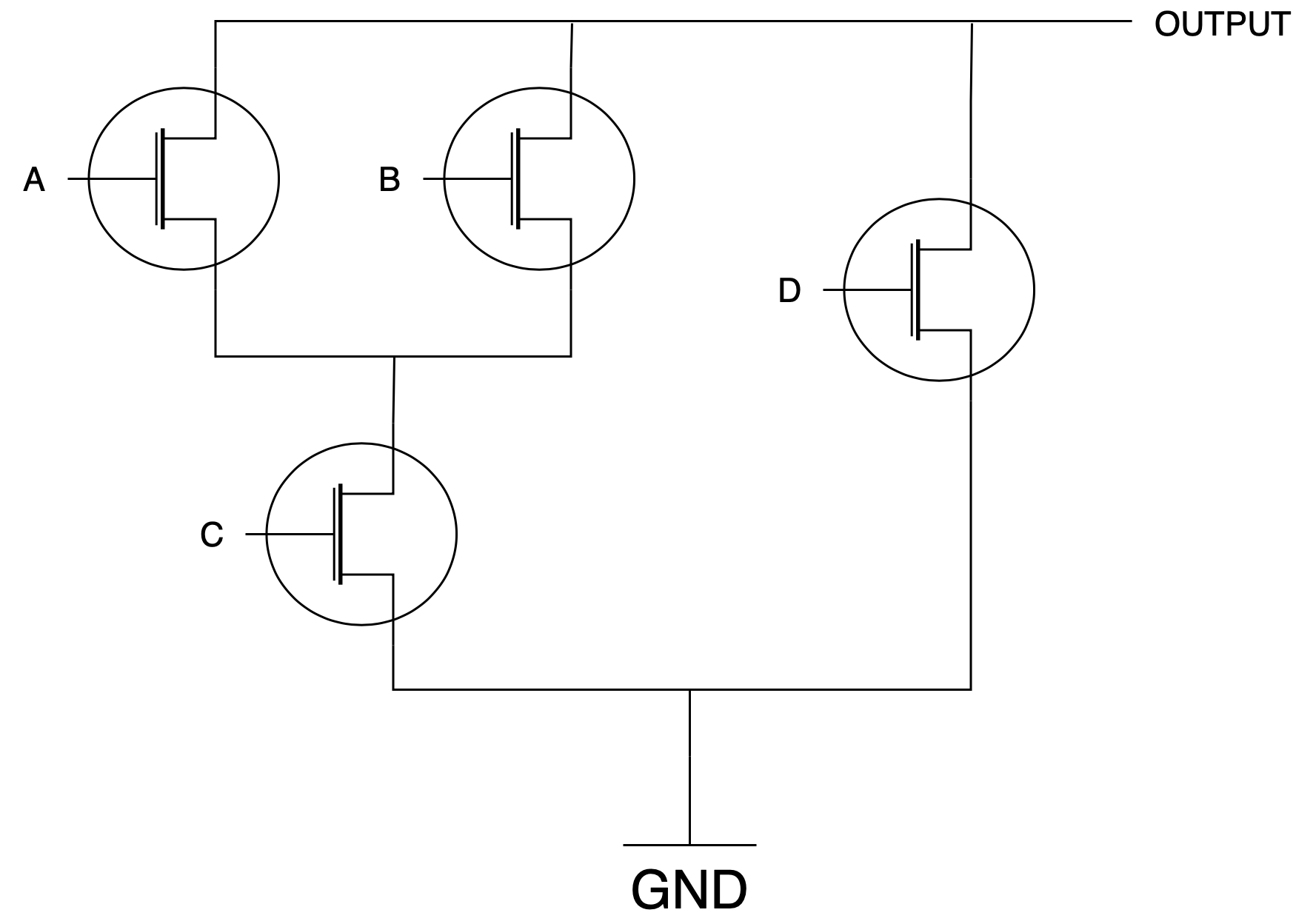
- What is the correct schematic for the pullup circuitry?
- Assuming the pullup circuitry is designed correctly, what is the logic function (boolean function) implemented at this gate?
- Assuming the pullup circuitry is designed correctly, when the output of the CMOS gate above is a logic “0” in the steady state, what would we expect the voltage value of the output terminal to approximately be? What would be the approximate voltage output value if the output were a logic
1?
- The output for the pullup circuitry is the inversion of the output of the pulldown circuitry:
$$\overline{(A+B) C + D} = (\overline{A} \text{ }\overline{B} + \overline{C}) \overline{D}$$
We don't need to add inverter in the inputs. Convince yourself that this is true by tracing some input combinations to the output terminal.

- From the pulldown diagram, it seems like the output is 0 if D is 1, or A and C is 1, or B and C is 1. Therefore, the output for the gate is the inverse of the expression of the pulldown circuitry, which is the output of the pullup circuitry above: $$\overline{(A+B) C + D} = (\overline{A} \text{ }\overline{B} + \overline{C}) \overline{D}$$
- The voltage of the output terminal at `0` steady state is `0` (GND). The voltage of the output terminal at `1` steady state is VDD's voltage.
Simplifying a Rather Complicated Boolean Expression (Intermediate)
Simplify the following boolean expression:
\[\begin{aligned} Y = &AB \bar{C} \bar{D} + AB \bar{C}D + \\ & \bar{A} \bar{B}CD + \bar{A}BCD + \\ & ABCD + A\bar{B}CD + \bar{A}\bar{B}C \bar{D} + \\ & ABC \bar{D} + A\bar{B}C \bar{D} \end{aligned}\]
The final simplified form is $$Y = AB + CD + \bar{B}C$$
The steps are as follows:
$$\begin{aligned}
Y &= AB \bar{C} \bar{D} + AB \bar{C}D + \bar{A} \bar{B}CD + \bar{A}BCD + ABCD \\
& + A\bar{B}CD + \bar{A}\bar{B}C \bar{D} + ABC \bar{D} + A\bar{B}C \bar{D}\\
&= AB\bar{C} + \bar{A}CD + ACD + \bar{B}C\bar{D} + ABC\bar{D}\\
&= CD + AB\bar{C} + \bar{B}C\bar{D} + ABC\bar{D}\\
&= C(D + \bar{B} \bar{D}) + AB(\bar{C} + C\bar{D} )\\
&= C(D + \bar{B} ) + AB(\bar{C} + \bar{D} )\\
&=CD + C\bar{B} + AB(\overline{CD} )\\
&= CD + C\bar{B} + AB
\end{aligned}$$
Convince yourself that the simplified form allows you to make a cheaper and smaller combinational logic device (because we use less number of gates). If you have your own method and can't seem to reconcile between the given answer and your answer, apply consensus theorem (scroll to the said theorem). You can also use online truth table tools to confirm that the truth table of your boolean expression and the above boolean expression is equivalent.
CMOS Gate Design (Challenging)
Anna Logue, a circuit designer who missed several early 6.004 lectures, is struggling to design her first CMOS logic gate. She has implemented the following circuit:

Anna has fabricated 100 test chips containing this circuit, and has a simple testing circuit which allows her to try out her proposed gate statically for various combinations of the A and B inputs.
She has burned out 97 of her chips, and needs your help before destroying the remaining three. She is certain she is applying only valid input voltages, and expects to find a valid output at terminal C. Anna also keeps noticing a very faint smell of smoke.
- What is burning out Anna’s test chips? Give a specific scenario, including input values together with a description of the failure scenario. For what input combinations will this failure occur?
- Are there input combinations for which Anna can expect a valid output at C? Explain.
- One of Anna’s test chips has failed by burning out the pullup connected to A as well as the pulldown connected to B. Each of the burned out FETs appears as an open circuit (no connection), but the rest of the circuit remains functional. Can the resulting circuit be used as a combinational device whose two inputs are A and B? Explain its behavior for each combination of valid inputs.
- In order to salvage her remaining two chips, Anna connects the A and B inputs of each and tries to use it as a single-input gate. Can the result be used as a single-input combinational device? Explain.
- When: `A=0, B=1` or `A=1, B=0`, it means that there's a connection between VDD and GND. This caused the gate to short circuit, and hence its burning out.
- Yes, when: `A=1, B=1`, then `C==0`. When `A=0, B=0`, then `C==1`. This happens when the pullup and pulldown circuit are not both `ON` (active) at the same time.
- No. When `A=1, B=0`, then the circuit will burn out again since the pullup and pulldown will be `ON` (active), thus causing a short circuit and burning out the circuit. Also, the output is **not** defined when: `A=0, B=1`. This is because **neither** the pullup or pulldown are active.
- Yes. It exhibits the behavior of an inverter, i.e: A and B are connected to the same `Vin`.
Another Boolean Minimisation (Basic)
A certain function F has the following truth table:
\[\begin{matrix} A & B & C & F \\ \hline 0 & 0 & 0 & 1\\ 0 & 0 & 1 & 0\\ 0 & 1 & 0 & 0\\ 0 & 1 & 1 & 1\\ 1 & 0 & 0 & 1\\ 1 & 0 & 1 & 1\\ 1 & 1 & 0 & 0\\ 1 & 1 & 1 & 1\\ \hline \end{matrix}\]Answer the following questions based on the truth table:
-
Write a sum-of-products expression for F.
- Write a minimal sum-of-products expression for F. Show a combinational circuit that implements F using INV and OR, and AND gates. Then implement it using only NAND gates.
- Implement F using one 4-input MUX and inverter.
- Write a minimal sum-of-products expression for NOT(F).
- Sum-of-products expressionf or F is: $$\overline{A}\text{ }\overline{B}\text{ }\overline{C} + \overline{A}BC + A \overline{B}\text{ }\overline{C} + A \overline{B}C + ABC$$
- The minimal sum of products is: $$\overline{B}A + \overline{B} \text{ } \overline{C} + BC$$ You can draw a combinational circuit of this by adding an input to a big OR gate for every '+', INV (where necessary for negated input) with AND gate for every *pair* of input in the minimal sum of products:

To turn AND and ORs into just NANDs, we can do this in two steps. First, turn the AND into NAND and add an inverter:

Then apply DeMorgan law:

- If we use A and B as the select inputs for the MUX, then the four data inputs of the MUX should be tied to one of `0` (ground), `1` (VDD), `C` or `NOT C`. The following is one of the correct schematics that implement this function (there are other acceptable answers as well). Note that by changing the connections on the data inputs to the MUX, we could implement any function of A, B and C. Another acceptable (and simpler) answer involves having two 4-input MUXes with `A` and `B` as selector each, reflecting their values when `C==0` and `C==1` respectively, and a 2-input MUX with C as its selector, and the outputs of the 4-input MUXes to each of the input terminals of the 2-input MUX. You're definitely not expected to come up with fancy circuitry design as the given answer below.

- We can just write *sum of product* for rows that results the `0`s in the table above, and then reduce the expression into: $$\overline{F} = B \overline{C} + \overline{A} \text{ } \overline{B} C$$
Reading Karnaugh’s Map (Basic)
Given the following Karnaugh’s Map, write its simplified boolean equation.
The minimised boolean expression is: $$AD + \bar{B}\bar{C} + \bar{B} \bar{D}$$ They're obtained from these **three** boxes:
- on the lower right corner (row 3 and 4, with column 3 and 4),
- on the sides (row 1 and 2, with column 1 and 4), and
- on the four corners (row 1 col 1, and row 1 col 4, and row 4 col 1, and row 4 col 4).
The FPGA (Challenging)
The Xilinx 4000 series field-programmable gate array (FPGA) can be programmed to emulate a circuit made up of many thousands of gates; for example, the XC4025E can emulate circuits with up to 25,000 gates.
The heart of the FPGA architecture is a configurable logic block (CLB) which has a combinational logic subsection with the following circuit diagram:

There are two 4-input function generators and one 3-input function generator, each capable of implementing an arbitrary Boolean function of its inputs.
The function generators are actually small 16-by-1 and 8-by-1 memories that are used as lookup tables. When the Xilinx device is programmed these memories are filled with the appropriate values so that each generator produces the desired outputs.
The multiplexer select signals (labeled Mx in the diagram) are also set by the programming process to configure the CLB. After programming, these Mx signals remain constant during CLB operation.
The following is a list of the possible configurations proposed:
(a). An arbitrary function F of up to four unrelated input variables, plus another arbitrary function G of up to four unrelated input variables, plus a third arbitrary function H of up to three unrelated input variables.
(b). An arbitrary single function of five variables.
(c). An arbitrary function of four variables together with some functions of six variables. Characterize the functions of six variables that can be implemented.
(d). Some functions of up to nine variables. Characterize the functions of up to nine variables that can be implemented.
(e). Can every function of six inputs be implemented? If so, explain how. If not, give a 6-input function and explain why it can’t be implemented in the CLB.
For each configuration indicate how:
- Each the control signals (
MA,MB,MC,MD, andME) should be programmed? - Which of the input lines (
C1-C4,F1-F4, andG1-G4) are used? - And what output lines (
X,Y, orZ) the result(s) appear on?
Video explanation here: part a & b, part c, d, & e.
- Let `X = F(F1, F2, F3, F4)` be the function of four variables with the four inputs connected to node `F1-F4`, `Z = G(G1, G2, G3, G4)` be another function of four variables with the four inputs connected to node `G1-G4`, and `Y = H(C1, C2, C3)` be the function with three unrelated input variables with the three inputs connected to node `C1-C3` in the diagram above. The necessary control signals are:
- `MA` = 1
- `MB` = 1
- `MC` = 0 (select `C1`)
- `MD` = 1 (select `C2`)
- `ME` = 2 (select `C3`)
- Let `Y = F(A1, A2, A3, A4, A5)`, where `A1` to `A5` are the five input variables which we can **map** to the input nodes in the diagram above. Let input `A1-A4` be connected to node `F1-F4` and `G1-G4` (they're connected to the same 4 inputs) and A5 be connected to node `C1`. This can be implemented using both 4-input logic functions, and selecting between the two outputs with the 3-input logic function.
- `Z = f(A1, A2, A3, A4, 0)`,
- `X = f(A1, A2, A3, A4, 1)`,
- `Y = Z` if `A5=0`, else `Y = X`
The necessary control signals are:- `MA` = 0
- `MB` = 0
- `MC` = X (value doesn't matter)
- `MD` = X (value doesn't matter)
- `ME` = 0 (select C1)
- Let `Z = G(G1, G2, G3, G4)` be the function of the 4 variables, so the four inputs are connected directly to node `G1-G4`. Then, let `X = F(F1, F2, F3, F4)` and let `Y = H(C1, C2, X) = H(C1, C2, F(F1, F2, F3, F4))`. The functions of six variables which can be implemented (along with the 4-variable function) are all those functions that can be **re-written** (decomposable) as the function H with 3 variables. The inputs to this function of three variables must be 2 of the original variables (plugged at nodes `C1`, `C2`) and some function of the remaining four variables (plugged at nodes `G1-G4`).The necessary control signals are:
- `MA` = 0
- `MB` = 1
- `MC` = X (value doesn't matter)
- `MD` = 0 (select C1)
- `ME` = 1 (select C2)
An example of decomposable function in this case is `H = (C1 XOR C2) AND (F1 OR F2 OR F3 OR F4)`. There's no complex interaction between `C` and `F` variables. On the other hand, the following function is not decomposable to fit the structure of `H` required above: `H = (F1 XOR F2) AND (F3 OR C1) AND (NOT F4 OR C2)`. This function intertwines the C variables with the F variables in a way that their outputs are dependent on each other's values. For example, the outcome of the operation `F3 OR C1` depends on both `F3` and `C1`, which means that the value of `C1` directly influences how `F3` contributes to the overall function and thus creating dependency between them. It won't be possible to encapsulate these two variables separately as either purely `C1`, `C2` inputs or as `F(F1, F2, F3, F4)` output in `H`. - Let: `X = F(F1, F2, F3, F4)`, `Z = G(G1, G2, G3, G4)`, `Y = H(C1, X, Z) = H(C1, F(F1, F2, F3, F4), G(G1, G2, G3, G4))`. The 9 inputs are connected to node `F1-F4`, `G1-G4`, and `C1`. The functions of nine variables that can be implemented are all those functions that can be re-written as the function `H` consisted of these 3 variables: `C1`, `F`, and `G`. The inputs to this three-variable function will be **one** of the original variables, plus **two** separate functions of 4 variables `F1-F4`, `G1-G4` (these two 4-variable functions will have the remaining 8 original variables as inputs).
- `MA` = 0
- `MB` = 0
- `MC` = X (value doesn't matter)
- `MD` = X (value doesn't matter)
- `ME` = 0 (select C1)
- The functions of 6 variables which we can implement must be of the form: `Y = C(C1, C2, F(F1,F2,F3,F4))` or the form of `Y = C(C1,F(F1, F2, F3, F4), G(G1, G2, G3, G4))`. This second function will have some **overlap** between `C1`, `F1-4`, and `G1-4`; that is some variables will be connected to **multiple** inputs.
Essentially, the functions we are able to implement are only those for which we can factor a set of 4 variables out of the equation. For example, the following function cannot be implemented by the CLB: `Y = A1A2A3A4A5 + A1A2A3A4A6 + A1A2A3A5A6 + A1A2A4A5A6 + A1A3A4A5A6 + A2A3A4A5A6` (Y is `1` only if there is one `0` in the input). This function cannot be broken down into either of the forms mentioned above.
This function says that `Y` is `1` if and only if these inputs are given as `A1-A6`: `111110`, or `111101`, or `111011`, or `110111`, or `101111`, or `011111`, or `111111`. However suppose `A3-A6` are plugged as `F1-F4`, and `A1, A2` are plugged into `C1, C2` in the FPGA. If you supply `A3-A6` as `0111`, it should output a `1` as the output of `F` due to the clause: `A1A2A4A5A6`. Then, if you supply `C1=0, C2=1`, it will output a `1` as well at `Y` due to the clause: `A2A3A4A5A6`. This effectively means `010111` gives a `1` which violates the condition for `Y`, which turns `1` only if there exist one `0` in the input. Hence the FPGA cannot implement this particular 6-variable function.