 50.002 CS
- Objectives
- Submission
- Starter Code
- Related Class Materials
- Combinational Logic Foundations
- Implementation
- First Principles Before Generalisation
- Checkoff
- Summary
- Appendix
50.002 Computation Structures
Information Systems Technology and Design
Singapore University of Technology and Design
Lab 2: Combinational Logic
Objectives
By the end of this lab, you should be able to:
- Turn informal descriptions of small combinational circuits into truth tables, Boolean equations, and gate level schematics.
- Implement a 1 bit full adder using primitive Boolean operators only, and explain how cascading full adders produces an N bit ripple carry adder.
- Use Lucid parameters and
repeatto generate regular hardware structure at compile time, and contrast this with software style loops that execute over time. - Describe the behavior of 2 to 1 and 4 to 1 multiplexers, and construct a 4 to 1 MUX hierarchically from 2 to 1 MUXes.
- Describe the behavior of 1 to 2 and 2 to 4 decoders, including one hot outputs, and construct a 2 to 4 decoder hierarchically from 1 to 2 decoders.
- Correctly use Lucid bit selection and bit range selection, and avoid width mismatches and off by one errors when wiring buses.
- Use Lucid module arrays for repeated structures such as multi bit adders and understand that you index ports of the array, not instances in an object oriented sense.
- Interpret
ifandcasein Lucid as specifications of combinational selection logic, and relate them directly to MUXes, decoders, and enable signals.
Submission
Complete the Lab 2 checkoff (2%) with your Cohort TA before the end of next Friday, 6PM (unless otherwise stated). The checkoff is assessed individually, but you should attend together with your project team so that everyone in the group understands the full workflow and expectations for the 1D project.
Complete questionnaire on eDimension as well (2%).
Starter Code
There’s no starter code for this lab. You simply need to have Alchitry Labs V2 installed. You don’t need Vivado for this lab, we are only going to run simulations.
Consult FPGA resources listed here before coming to the lab or after the lab to enhance your knowledge on FPGA programming in general. This will greatly accelerate the quality of your 1D & 2D project.
Related Class Materials
The lecture notes on logic synthesis and CMOS technology are closely related to this lab.
| Lecture notes topic | Lab 2 part |
|---|---|
| Boolean algebra, truth tables, gate-level synthesis (from Logic Synthesis) | Full adder design, MUX & decoder Boolean expressions and gate implementations |
| Universal-gate theory, minimisation, SOP/NAND/NOR equivalence | Allowing FA implementation using NAND-only/NOR-only as alternative forms |
| Hierarchical composition (small modules to larger modules) | Building 4-to-1 MUX from 2-to-1 MUXes; 2-to-4 decoder from 1-to-2 decoders; RCA from multiple FAs |
| Combinational logic abstraction + static discipline + clean voltage-levels (from CMOS technology) | Treating all signals as 0/1, driving all outputs cleanly, no floating outputs, combinational always blocks |
| Propagation delay and critical path (CMOS timing) | Ripple-carry adder’s inherently linear carry chain, it provides insight for timing and scalability |
Combinational Logic Foundations
Before touching the FPGA, we will translate several logic requirements into Boolean expressions and circuits. Afterwards, we will describe that hardware in HDL and run it on the Alchitry lab simulator. If all works well, we shall build and flash it to the FPGA.
In this lab, we will build three core combinational logic devices: the full adder, the multiplexer (both 2 to 1 and 4 to 1), and the decoder (both 1 to 2 and 2 to 4).
These are the most basic non-trivial building blocks of a CPU, the computational “brain” found in microcontrollers, general-purpose computers, GPUs, and other digital systems.
This is the first step in learning how to construct actual compute units from fundamental logic instead of treating them as black boxes.
Full Adder
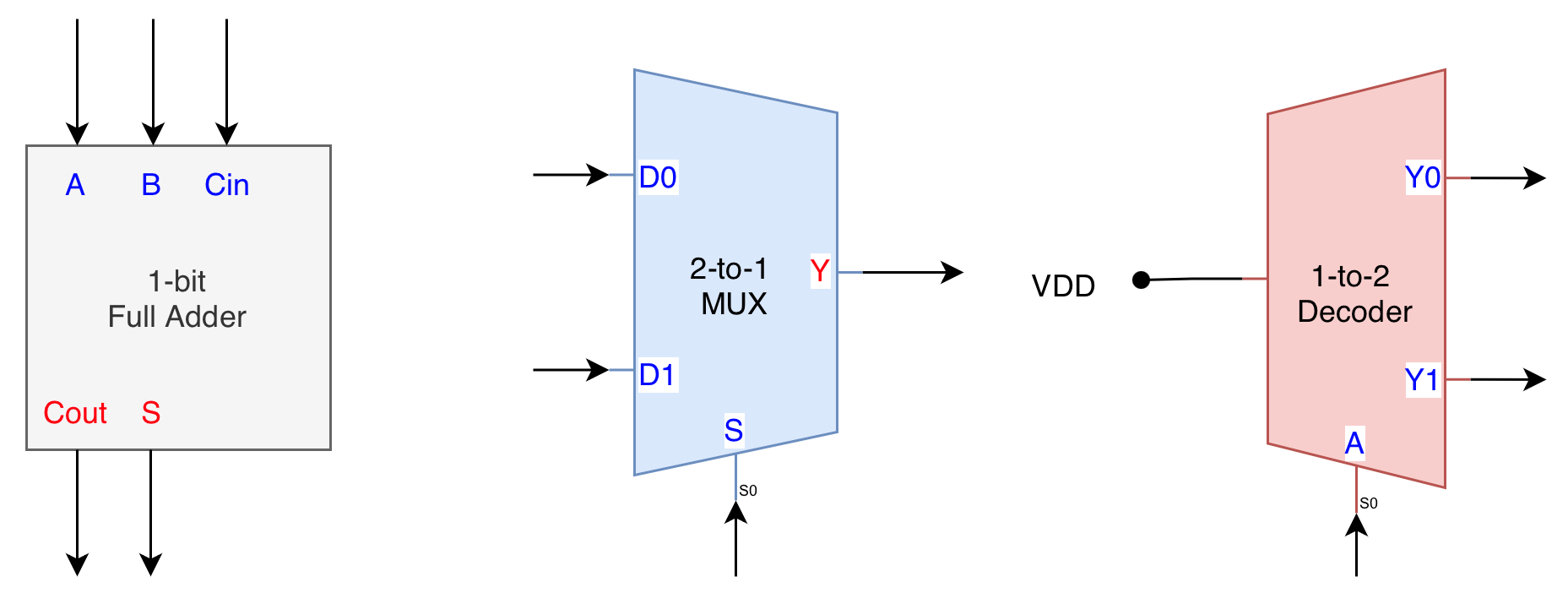
The first combinational logic circuit we are going to build is the full adder (FA). This is the smallest non-trivial arithmetic block in digital systems. Its only job is to add three 1-bit values together and produce a 1-bit sum and a 1-bit carry.
This full adder is a fundamental building block of the ALU (lab in later weeks), which is the computational core of a CPU (which is our goal in learning this course). By building a full adder, we are starting from the smallest unit that will later scale into an ALU and ultimately a working CPU datapath.
The FA module has 3 inputs (A, B, and Ci) and 2 outputs (S and Co). The logic equations and truth tables for S and Co are shown below. The logic equation is derived from the truth table.
| A | B | Ci | S | Co |
|---|---|---|---|---|
| 0 | 0 | 0 | 0 | 0 |
| 0 | 0 | 1 | 1 | 0 |
| 0 | 1 | 0 | 1 | 0 |
| 0 | 1 | 1 | 0 | 1 |
| 1 | 0 | 0 | 1 | 0 |
| 1 | 0 | 1 | 0 | 1 |
| 1 | 1 | 0 | 0 | 1 |
| 1 | 1 | 1 | 1 | 1 |
Logic Equation:
\[\begin{align} S &= A \oplus B \oplus C_{i} \\ C_{o} &= A \cdot B + A \cdot C_{i} + B \cdot C_i \end{align}\]The above is not the only way we can write the boolean expression of the FA module.
You can express it using the sum of products method (ANDs and ORs for
Sinstead of XORs). You can also build it using only the NAND gates or only the NOR gates since they are universal gates.
Intuitively, you can think of it as binary column addition:
- Add
AandB - Then add the incoming carry
Ci - If the total is
0or1, it goes toS - If the total is
2or3, it “overflows” and produces a carry (Co=1)
Adding two 1-bits together doesn’t seem much at first. But in order to make an N-bit adder later on, we simply cascade N FA modules together. We will get there later.
Multiplexers (MUX)
The next combinational building block is the multiplexer (MUX). While the full adder computes, the MUX selects. You will use MUXes everywhere in an ALU and datapath to choose which value should flow forward.
2:1 MUX
A 2:1 MUX has:
- Two data inputs:
D0,D1 - One select input:
S - One output:
Y
MUX logic recap
- If
S = 0, outputYshould beD0- If
S = 1, outputYshould beD1
The boolean expression for a 2-to-1 MUX is: \(Y = \overline{S} \cdot D_0 + S \cdot D_1\)
This is a very compact sum of products expression. From this single line, you can directly draw the gate level implementation:
- One inverter for
S - Two AND gates for the product terms
- One OR gate to combine
You can think of a 2:1 MUX as a controlled digital switch (an if logic). The select line S decides which data input is connected to the output. In the ALU later, the MUX will choose between different operation results or between different sources for the same bus.
For multi bit signals, you simply apply the same equation bitwise. For example, a 4 bit 2:1 MUX takes D0[3:0], D1[3:0], and S, and produces Y[3:0] where each bit of Y is selected by the same S.
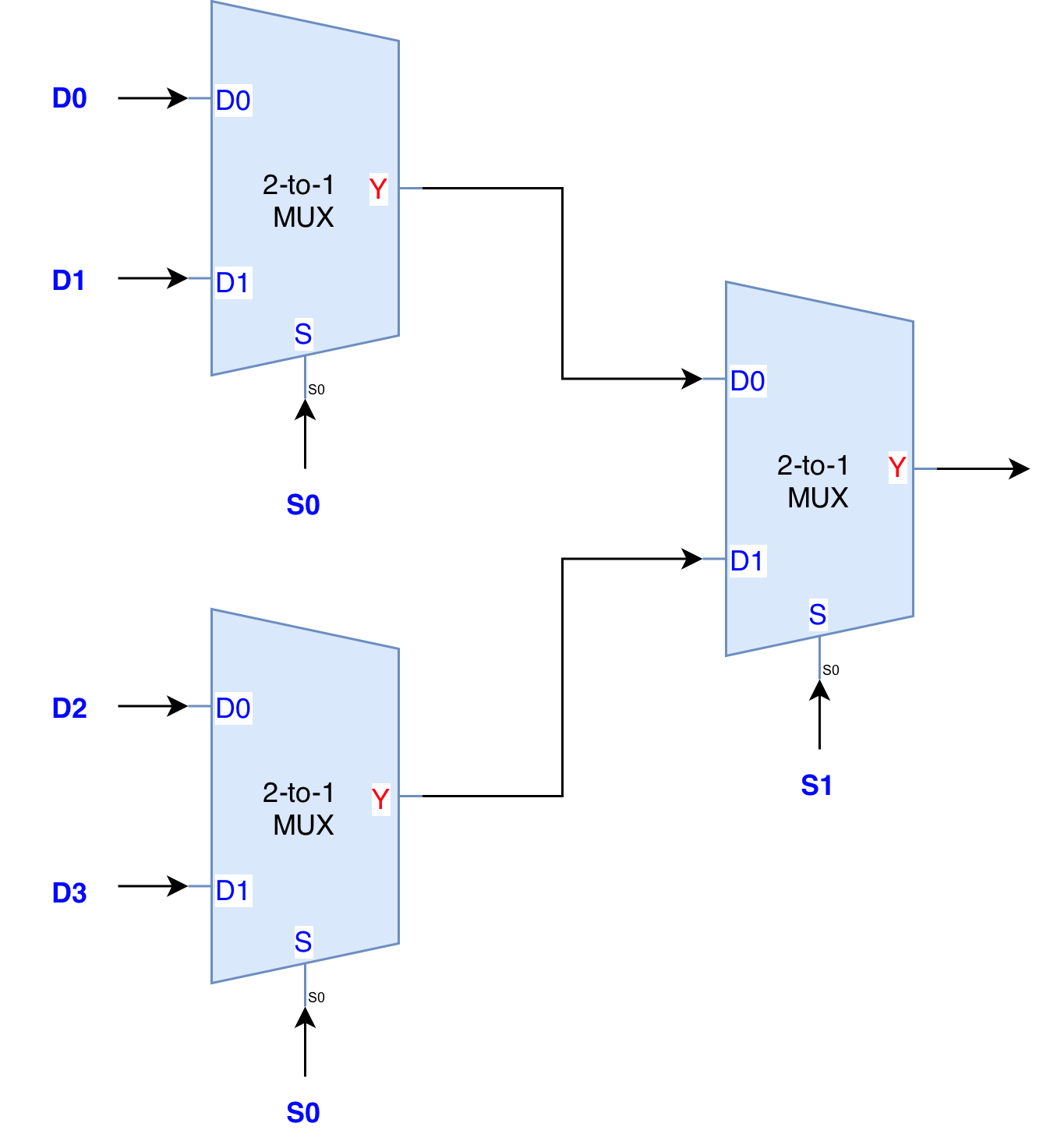
From 2:1 MUX to 4:1 MUX
A 4:1 MUX is simply an extension to the 2:1 MUX. It has:
- Four data inputs:
D0,D1,D2,D3 - Two select inputs:
S1,S0 - One output:
Y
The truth table now uses the 2 bit select (S1 S0) to choose which Di appears at Y. For example:
S1S0 = 00selectsD0S1S0 = 01selectsD1S1S0 = 10selectsD2S1S0 = 11selectsD3
You can write the Boolean equation:
\[\begin{align} Y &= \overline{S_1} \cdot \overline{S_0} \cdot D_0 \\ & + \overline{S_1} \cdot S_0 \cdot D_1 \\ & + S_1 \cdot \overline{S_0} \cdot D_2 \\ & + S_1 \cdot S_0 \cdot D_3 \end{align}\]But for the lab, it is more important that you see how to construct a 4:1 MUX from smaller 2:1 MUXes that you already understand. A standard structure is:
- First stage: two 2:1 MUXes select between
(D0, D1)and(D2, D3)usingS0 - Second stage: a final 2:1 MUX selects between those two intermediate results using
S1
Composition
This bottom up construction is the same philosophy we use for the CPU datapath. We do not design a giant block from scratch. We design small, verified modules (like 2:1 MUXes and full adders) and then compose them systematically into larger components such as 4:1 MUXes, ALUs, and eventually the whole CPU.
This is why static discipline is so important. It allows us to compose large and complex digital circuits from smaller components and they will all communicate perfectly without loss of information.
Decoder
A decoder is another standard combinational block. While a MUX selects one of many inputs to drive a single output, a decoder activates exactly one of many outputs based on the input code. It essentially converts a binary code into a one hot output.
A one-hot encoding means that exactly one signal line is HIGH (1) at any given time, while all others are LOW (0). For a 2-to-4 decoder, this means only one of Y0, Y1, Y2, or Y3 can ever be 1 for a valid input, and the rest must be 0. This is useful for selecting or enabling exactly one component in a larger system, such as choosing which register to write to or which operation to activate in a control unit.
1 to 2 Decoder (with Enable)
A decoder with enable is also called a demultiplexer in some other texts.
The simplest form of a decoder is the 1-to-2 decoder. It takes a single binary input and activates exactly one of two outputs.
A 1:2 Decoder has:
- Two data inputs:
A,V(the enable) - Two outputs:
Y0,Y1(one-hot)
decoder logic recap
- If
A = 0, outputY0should beV, whileY1should be0- If
A = 1, outputY1should beV, whileY0should be0
The Boolean equations are:
\[\begin{align} Y_0 &= \overline{A} \cdot V \\ Y_1 &= A \cdot V \end{align}\]2 to 4 Decoder
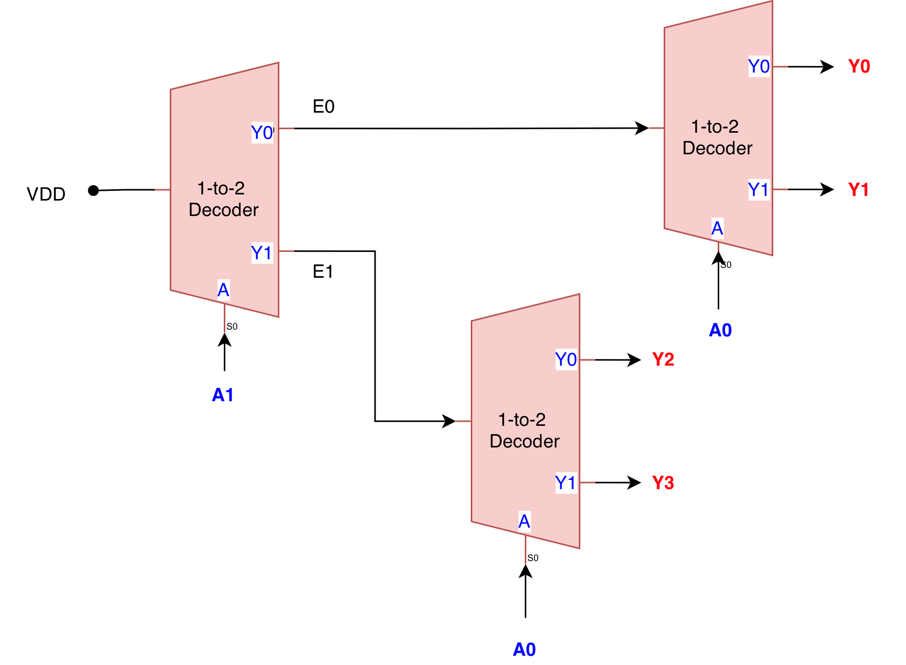
A 2-to-4 decoder converts a 2-bit binary input into four one-hot outputs. It can be constructed hierarchically using three 1-to-2 decoders arranged in two stages. It has:
- Two data input:
A0,A1 - Four outputs:
Y0,Y1,Y2,Y3(one-hot) - If you have an enable, then one more data input
V. For simplicity, we just connect it toVDD
Conceptual construction:
- A 1-to-2 decoder first acts on the MSB (
A1), producingE0andE1 - These two signals enable two separate 1-to-2 decoders that act on the LSB (
A0):- The first produces
Y0andY1whenE0 = 1 - The second produces
Y2andY3whenE1 = 1
- The first produces
This results in exactly one output being asserted for every possible input combination.
When building a larger decoder from smaller modules, do not confuse port names with signal identity. For example, a 1-to-2 decoder module may have output ports named Y0 and Y1, but when that module is instantiated inside a 2-to-4 decoder, those ports can be connected to signals such as Y2 and Y3. The module’s internal port names do not define the meaning of the signal in the larger design. Only the actual wire it is connected to determines its role in the system.
Signal Mapping (trace it from the circuit diagram to test your understanding):
A1A0 = 00:Y0 = 1,Y1 = Y2 = Y3 = 0A1A0 = 01:Y1 = 1,Y0 = Y2 = Y3 = 0A1A0 = 10:Y2 = 1,Y0 = Y1 = Y3 = 0A1A0 = 11:Y3 = 1,Y0 = Y1 = Y2 = 0
The Boolean equations are therefore:
\[\begin{align} Y_0 &= \overline{A_1} \cdot \overline{A_0} \\ Y_1 &= \overline{A_1} \cdot A_0 \\ Y_2 &= A_1 \cdot \overline{A_0} \\ Y_3 &= A_1 \cdot A_0 \end{align}\]Each output is a single product term. No summation is required because exactly one output is asserted in any given row of the truth table.
Decoder Usage
A decoder can be seen as the structural opposite of a multiplexer. A multiplexer uses a binary code to select one input. A decoder uses a binary code to activate one output. In a CPU, decoders are used as control logic, for example selecting a target register or enabling a specific ALU operation from an opcode.
With the full adder, MUXes, and decoders, we now have the core combinational patterns that will be reused continuously when we assemble the ALU and CPU datapath.
Implementation
Now lets implement each of the combinational logic module above. Create a new project in Alchitry Labs using this template:

Remember to always select the base project with pulldowns. This is to ensure that the board receives a valid low when input buttons are not pressed (which maps to invalid input if a pulldown internal resistor is not present). If you’re interested to know more, read this.
Then we will build the modules in the following order
- 1-bit full adder
- N-bit adder using full adder
- Mux2
- Mux4 using Mux2
- Decoder1to2
- Decoder2to4 using Decoder1to2
Testing reminder
As in Lab 1, always simulate your design before thinking about the FPGA:
- Write or complete the module.
- Instantiate the module in the top module (
alchitry_top) and open the simulator. - Use the switches to drive a small set of input patterns. Connect the outputs to some LEDs.
- Check that the outputs match the truth table / behaviour specified above.
If needed, refer back to Lab 1 for the detailed steps on how to run the Alchitry simulator and connect signals to IO.
Important Lucid Operators
We assume that you have done your due diligence to scan through the Lucid reference guide and understand how basic boolean operators (bitwise, reduction, etc) works. If not, read this Appendix first.
1-bit Full Adder
You are NOT allowed to use the built-in ‘+’ operator in Lucid for this lab and for your 1D project. In fact, you are not allowed to use many arithmetic operators for your project (see later labs). High-level arithmetic operators are intentionally restricted. You must construct functionality from Boolean logic and primitive modules, since the objective of this course is to understand the internal structure and behaviour of digital systems, not to abstract it away.
For instance, writing
sum = a + b + cihides the structure of half-adders and full-adders and bypasses Boolean reasoning.You must implement the full adder using:
- Boolean expressions
- AND, OR, NOT, XOR (or NAND/NOR only for bonus)
The purpose of this lab is to expose the actual hardware structure of addition, not to hide it behind a high-level operator.
Below is a proposed interface:
   module fa (
      input a,
      input b,
      input cin,
      output s,
      output cout
   ) {
      always {
         s = 0
         cout = 0
      }
   }
Test: Full Adder
In the simulator:
- Check through all 8 input combinations (
a,b,cinfrom000to111) using some switch. - Map
s,coutto two of the LEDs - Check that (
s, cout) exactly matches the truth table in the “Full Adder” section. - Pay attention to the carry cases: 0+1+1, 1+1+0, 1+1+1.
For example, we use io_led[1:0] to show cout, s and io_dip[2:0] to enter cin, b, a.

Then, test all combinations:

Ripple Carry Adder
We can cascade FA units to form a Ripple-Carry Adder (RCA). The module performs the addition of two one-bit inputs (A and B) incorporating the carry in from the previous stage (Ci). The result appears on the S output and a carry (Co) is generated for the next stage.
A possible schematic for a 4-bit adder is shown below:
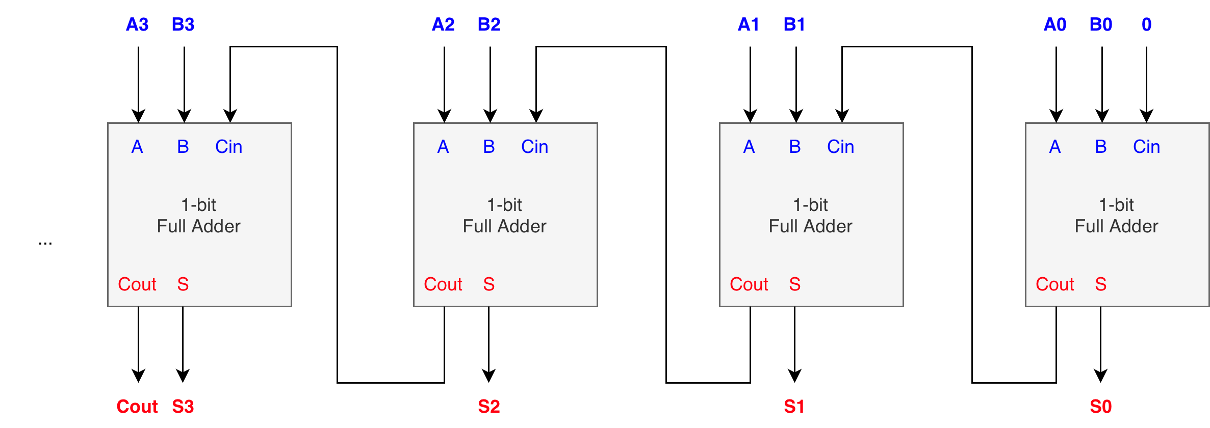
What do you think is the tcd and tpd of this 4-bit adder?
You can pretty much generalise it into N-bit adder. A common value is 32-bit or 64-bit adder. Modern computers typically support 64 bits. Simpler microcontrollers might only support 32 bits.
This module requires a parameter so that we can instantiate it with different values. Complete the implementation below.
module rca #(
    SIZE = 32 : SIZE > 1
)(
    input a[SIZE],
    input b[SIZE],
    input cin,
    output s[SIZE],
    output cout
) {
    always {
        s = 0
        cout = 0
    }
}
The
SIZEparameter in the rca module does not make the adder dynamically resizable at runtime. The parameter increases code flexibility, not hardware flexibility.It is a compile-time constant, fixed when the design is built and synthesised. This means the hardware is fully determined before the FPGA is programmed.
The purpose of
SIZEis simply to let you reuse the same module definition for different fixed widths by changing a single value at instantiation time, not to create a variable-width adder during execution.
Bit “indexing”: big:small
In hardware description languages, bit ranges are written in big:small order:
sig data[8] // declaration

// usage options
// assume out is an 8-bit port
out = data  // without bit selector
out = data[7:0]   // with bit selector, to select from bit 7 (MSB) down to bit 0 (LSB)
out = c{3b0, data[4:0]} // with bit selector and array concatenation
This is NOT the same mentality as Java, C, or Python arrays. In software:
array[0]usually means the first element- Indices increase left to right
- Index numbers describe position in memory
- In Python we have slicing:
array[3:8] # elements at index 3,4,5,6,7- That means “from index 3 up to but not including index 8.”
- This is completely unrelated to MSB/LSB or bit significance.
In HDL (not specific to Lucid):
data[7]is the most significant bit (MSB)data[0]is the least significant bit (LSB)- The numbers describe bit significance, not position in a list
So this:
data[7:4]   // upper 4 bits
data[3:0]   // lower 4 bits
means “HIGH bits” and “LOW bits,” not “later” and “earlier” in memory. The index selector will select all the indices from min to max including both.
This also means the following, since the “index” numbers describe bit weight, not list position.:
data[0]   // the 1’s place
data[1]   // the 2’s place
data[2]   // the 4’s place
...
data[7]     // most significant bit
In HDL, the index is a power of two, not a position in a list.
You should read the selector documentation first before proceeding.
Actually, “indexing” better described as bit selection and bit-range selection, not array indexing in the software sense.
data[3]is a bit selector. You are selecting a single bit.data[7:3]is a part-select or bit-range selector.sig data[8]is a bus declaration / range declaration.
Calling bit selection “array indexing” might import the wrong mental model from software and leads to confusion.
However, you will often hear people loosely say “indexing” a signal, for example data[3] or data[7:0]. Technically, in HDL this is better thought of as bit selection rather than array indexing in the software sense. The number refers to the significance and weight of a bit, not its position in a list in memory. For clarity, you should mentally treat it as a selector, even if people casually call it an index.
repeat statement
The repeat statement allows for a block of statements to be considered multiple times.
They take the following form:
repeat(i, count, start = 0, step = 1) {
    statements
}
From the documentation:
- Here
countis a constant expression indicating how many times the block of statements should be considered. - The arguments
startandstepare optional and have default values of0and1respectively. - The
iargument is an optional variable name that can be used inside the repeat block.- It will start with the value
startand increment by step each iteration of the loop to a final value ofstart + step * (count - 1). - It must start with a lowercase letter and can contain letters, numbers, and underscores. By convention, it is snake_case.
- It will start with the value
In Lucid, repeat is not a software-style loop. It does not execute over time. Instead, it is a code generator that replicates hardware structure multiple times during synthesis.
For example:
   module left_shift_1b #(
      SIZE = 8 : SIZE > 1
   )(
      input  in[SIZE],
      output out[SIZE]
   ) {
      always{
         // fill LSB with 0
         out[0] = 0

         // shift everything else left by 1
         repeat(i, SIZE-1) {
               out[i+1] = in[i]
         }
      }

   }
Explanation:
- Each iteration of
repeatcreates a new fixed wire connection fromin[i]toout[i+1] - All of these connections exist in parallel in the final hardware
- The index
iis resolved entirely at compile time, not at runtime - The design does not “shift” over time. The apparent shift is created purely by the static wiring pattern
- Changing
SIZEonly changes how many of these parallel connections are generated in hardware
This is equivalent to writing:
   always {
      out[0] = 0
      out[1] = in[0]
      out[2] = in[1]
      out[3] = in[2]
      out[4] = in[3]
      out[5] = in[4]
      out[6] = in[5]
      out[7] = in[6]
   }
repeat is a structural construction tool, not a behavioural one. It is fundamentally different from a software loop. You are describing how much hardware to build, not what sequence of operations to perform.
Hence, the repeat statement makes it ideal for building regular, repeated hardware patterns such as an N-bit ripple-carry adder, especially when N is defined only at compile time.
IDE Limitation
The following “theoretically identical” code will result in an error:
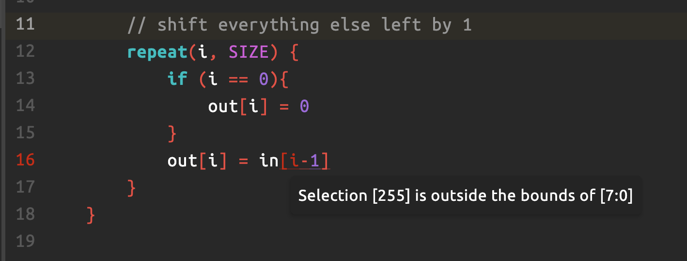
The IDE is not “smart” enough to see that the if protects the out-of-bounds access. The static checker only sees in[i-1] with i ranging from 0 to SIZE-1.
- At
i = 0that becomesin[-1]which is okay since Lucid V2 supports negative indices, but somehow the checker ran by the IDE in the repeat loop translated it to 255, which is obviously out of bounds, so it complains. - It does not analyse the
if (i == 0)and does not understand that the statement is effectively skipped for that index.
Conceptually the hardware is fine, but the tool cannot prove it, so you should rewrite the pattern so that the indices are always in range without relying on conditionals inside repeat.
HDL IDE Limitation
Most HDL tools do syntactic bound checking, not deep symbolic reasoning. They simply substitute the loop range and check the index expression mechanically. They do not attempt to prove that a conditional like
if (i == 0)prevents an illegal access. As a result:
- They flag
in[i-1]as an error because, in the general case,ican be0- They ignore the logic that would prevent that case at compile time
- They prefer simple, provably-safe index ranges
This is not unique to Lucid. You will see the same behaviour in Verilog, VHDL, and SystemVerilog tools as well.
The correct engineering response is to structure the loop bounds so the index is always valid, rather than relying on a conditional to protect it.
That is actually good practice in HDL anyway. It makes the hardware intention unambiguous to both the compiler and human readers.
Lucid Module arrays
In Lucid, we are selecting (indexing) PORTS, not instances, therefore when you write:
fa fa[SIZE]
…you are creating SIZE parallel full adder instances. However, the way you index them is slightly unintuitive at first.
The important rule:
You index the PORTS, not the module name. You write
fa.port[index], notfa[index].port.
For example:
fa fa[SIZE]

always {
    fa.a = a        // connect all A bits in one shot
    fa.b = b        // connect all B bits in one shot

    fa.cin[0] = cin // connect cin of instance 0
    // later: fa.cin[i+1] = fa.cout[i] inside a repeat
}
Here:
fa.ais a bus of inputs, oneafor each full adder instance.fa.a[i]refers to theainput of the i-th full adder.- The syntax
fa[0].ais not valid in Lucid becausefais not an array of objects in the OO sense. It is a single module array whose ports are vectorised.
Think of
fa.aas “all theawires of all the FAs bundled together.” Indexing picks one wire out of that bundle:fa.a[i].
Lucid vs Verilog
Note that this is not the same across HDL. In Verilog/SystemVerilog:
fa fa_array [0:SIZE-1] (...);

fa_array[0].cin = cin;
The difference lies in how modules are treated:
- Lucid treats
faas a vectorised module, where each port becomes a vector. You index ports:fa.a[i],fa.cout[i]. - Verilog/SystemVerilog treats
fa_arrayas an array of module instances. You index instances:fa_array[i].a,fa_array[i].cout.
This is an important conceptual distinction:
In Lucid, you index signals of a module array. In Verilog, you index the module instances themselves.
Test: Ripple-Carry Adder
You may test your RCA by instantiating it with a small SIZE, such as SIZE = 4:
- Test:
0001 + 0001: expect0010,cout = 0. - Test:
0011 + 0001: expect0100,cout = 0. - Test:
1111 + 0001: expect0000,cout = 1.
   // in alchitry_top
    rca rca(#SIZE(4))

    always {

      // connect some io_dip and io_led to rca ports
    }
We connect some dips and leds to the rca’s ports:

And test the addition logic:

2-to-1 MUX
Implement the 2-to-1 MUX module:
module mux2to1 (
    input data0,
    input data1,
    input s,
    output y
) {
    always {
        y = 0
    }
}
Note that we don’t use d0 or d1 to name the input variables because it’s a reserved keyword in HDL, that represent decimal 0 or decimal 1.
You may use the boolean logic as stated in the previous section, or to use conditional if or case statement in Lucid. Either way is permissible.
if statement
An if statement allows you to conditionally consider hardware behavior, something like if button X is pressed, then the device will output value Y, otherwise, the device will output value Z where Y,Z are N bit outputs.
They take the following form:
if (condition) {
    statements
} else {
    statements
}
If condition is true, meaning non-zero, then the statements in the first statements section are considered. If it is false, meaning zero, then the statements in the second statements section are considered.
When synthesised, this is not a flow of execution. There is no branching or time order like in software. Instead, the if–else is translated into combinational selection logic, equivalent to a multiplexer controlled by selector signal.
case statement
Similarly, the case statement provides a way to describe multiple conditional behaviours based on the value of a single expression.
It takes the following form:
case (condition) {
    VALUE_1:
        statements
    VALUE_2:
        statements
    ...
    default:
        statements
}
The condition expression is evaluated and compared against the provided values (VALUE_1, VALUE_2, etc) inside the case block.
Similarly, this is not a sequence of checks executed one after another. There is no branching or looping in time. Instead, the case statement is translated into combinational decoding and selection logic.
Concretely, it is equivalent to building:
- A decoder that turns the condition value into one-hot select signals
- A multiplexer (or OR-combine logic) that chooses which statement block drives the output
Parallel Existence
In other words, the hardware exists in parallel, and the case statement becomes:
- “Decode this binary input”
- “Enable exactly one output path”
- “Route that output to the destination”
Conditionals in hardware
In hardware, all possible paths already exist physically, and they are not created, destroyed, or traversed in time unlike in software system. The only thing that changes is which path is active, based on the input signals.
So when you write an if or a case statement in Lucid:
- You are not telling the computer to “go down one path”.
- You are not creating a sequence of decisions.
- You are describing which existing hardware path is enabled and which ones are disabled.
The condition or case value becomes a control signal that:
- Turns one path “on”
- Forces other paths “off”
- And determines which result is visible at the output
This is a very important concept that should be understood to understand the rest of the syllabus.
A useful analogy: All roads are already built. The selector (control, conditional) signal only changes which traffic light is green.
This is why if and case in a hardware description language ultimately become multiplexers, decoders, and enable signals in real circuitry. There’s no change the structure at runtime but they only change which part of the structure is being used at that moment.
4-to-1 MUX
Now instantiate three 2-to-1 MUXes to create 4-to-1 MUX:
module mux4to1 (
    input data0,
    input data1,
    input data2,
    input data3,
    input s0,
    input s1,
    output y
) {
    always {
        y = 0
    }
}
1-to-2 Decoder
Implement the 1-to-2 decoder module:
module decoder1to2 (
    input v,
    input a,
    output y0,
    output y1
) {
    always {
        y0 = 0
        y1 = 0
    }
}
2-to-4 Decoder
Afterwards, instantiate 3 of them to implement 2-to-4 decoder module:
module decoder2to4 (
    input v,
    input a0,
    input a1,
    output y0,
    output y1,
    output y2,
    output y3
) {
    always {
        y0 = 0
        y1 = 0
        y2 = 0
        y3 = 0
    }
}
Test: MUX and Decoder
Similarly, pick the switch and LEDs to test your MUX and decoder logic. You can be fancy and implement a “mode”. Here we use io_dip[2][7:6] as output enable, to route whether to display 4-to-1 MUX’s output or 2-to-4 decoder’s output:

    // in alchitry_top
    mux4to1 m
    decoder2to4 d

    ...

    always{

        // other connections

        // always driven
        m.data3 = io_dip[2][3]
        m.data2 = io_dip[2][2]
        m.data1 = io_dip[2][1]
        m.data0 = io_dip[2][0]
        m.s0 = io_dip[2][6]
        m.s1 = io_dip[2][7]

        d.a1 = io_dip[2][1]
        d.a0 = io_dip[2][0]
        d.v = 1b1

        // enable display accordingly
        if(io_dip[1][7]){
            io_led[2][7] = m.y
        }

        if (io_dip[1][6]){
            io_led[2][3:0] = c{d.y3,d.y2,d.y1,d.y0}
        }
    }
Here’s the test in action. We began by testing the multiplexer, then the decoder.

First Principles Before Generalisation
When learning HDL, resist the urge to over-engineer, over-refactor, or over-modularise immediately.
If you are new, you should first write the basic circuits out explicitly, even if it feels repetitive or boring. Mundane repetition is acceptable at this stage, because it forces you to see exactly which signals connect where.
Do not rush to create a fully generic “N-to-2^n decoder” or a super-parameterised Mux yet.
- Get the concrete 1-to-2 and 2-to-4 versions correct and readable first.
- Only then is it meaningful to generalise.
- Sometimes it is not even important to generalise because for instance, you’re not going to USE that many variations of MUX/decoder in your project in the first place. So who are you making it for?
- If it is for learning and you have free time on hand, great. Go ahead.
- But if it introduces bugs and frustration, that means your knowledge is not adequate yet. Stick to the basics. They always work with minimal errors.
Similarly, using AI tools to generate clever abstractions before you understand the syntax and semantics yourself is counterproductive. In 50002, the goal is not rapid prototyping. The goal is to internalise the basic building blocks of digital logic.
Component Library
In practice, most “common” hardware designs typically already exist as a library. In Alchitry labs, a generalised Decoder is provided for you.
There’s also an Encoder (not a MUX), which is a conceptual opposite of a decoder:
- A decoder takes a binary code and produces a one-hot output.
- Example: 2-bit input, 4 outputs, exactly one output is 1.
- An encoder takes (ideally) one-hot inputs and produces a binary code.
- Example: 4 inputs, 2-bit output that encodes which input is active.
Explore the component library before trying to re-invent the wheel yourself.
Pitfalls
Assigning mismatched dimension
The following statements are NOT equivalent:
 mux2to1.s[1:0] = 2x{s0}
 mux2to1.s[1:0] = s0
The first one assigned s0 to BOTH s ports. The second one is trying to drive a 2-bit slice with a 1-bit signal, i.e. it is a width-mismatched assignment.
mux2to1.s[1:0] = 2x{s0}explicitly builds a 2-bit bus{s0, s0}and assigns it tos[1:0]. Both instances sees0.mux2to1.s[1:0] = s0presents a 1-bit value on the right, but the left is 2 bits wide. In HDL this does NOT mean “replicates0twice.” The compiler will treat it as an invalid assignment with incompatible widths and try to fix it automatically padding it with more zeroes, because it expects the right-hand side to be 2 bits wide.
This is why you need to always MATCH signal width assignments. Otherwise, try not to be fancy and write each assignment out without selectors:
mux2to1.s[0] = s0
mux2to1.s[1] = s0
Consult Lab 1 if needed to recap about width mismatch.
Using + for OR instead of |
The following statements are NOT equivalent:
   out = x | y&z
   out = x + y&z
Module Array Indexing
In Lucid, you index signals of a module array, so you must write module_name.port[index] if you’d like to access individual signals of a module array. You need to understand that Alchitry’s Lucid is a custom HDL designed mainly for teaching and productivity, not for industry synthesis flows. This “vectorised module” idea is quite unusual, but should not be a problem once you get the concept. Our goal is not to memorize syntax here.
In Verilog/SystemVerilog, you index the module instances themselves, so you can write module_name[index].port.
Checkoff
Demo on Simulator (1%)
Demonstrate to your TA that your 4-bit RCA, 4-to-1 MUX, and 2-to-4 Decoder works on the simulator.
You can choose to use any LEDs/switches on the IO Shield.
QnA Protocol (1%)
During the checkoff, the TA will ask at most two questions about the code that you personally wrote. You have one attempt per question.
- If you answer the first question correctly, no second question will be asked.
- If you answer the first question incorrectly, you will be given exactly one more question.
Grading for QnA is therefore binary: 1% if you answer at least one correctly, 0% if you answer both incorrectly. This applies to ALL checkoffs in the future labs as well.
Schedule a checkoff with your TA anytime before the end of next week’s lab as a 1D group. The checkoff is graded individually but to aid logistics and to ensure everyone in the group is on the same page, you are required to attend the checkoff together as a 1D group. It will take about 15 minutes in total for the whole group to clear a checkoff on average.
Summary
In this lab we construct three core combinational building blocks from first principles: full adders, multiplexers, and decoders. We start with truth tables and Boolean equations, then implement them explicitly in Lucid without relying on high level arithmetic operators. We then scale the 1 bit full adder into a parameterised ripple carry adder, which is the backbone of a realistic ALU.
On the control side, we recapped MUXes and decoders as dual views of selection logic. You build a 4 to 1 MUX from smaller 2 to 1 MUXes and a 2 to 4 decoder from 1 to 2 decoders, reinforcing the design habit of composing larger circuits from small, verified modules. Throughout, you practice reading and writing Lucid in a hardware centric way: bit selection instead of array indexing, repeat as structural replication rather than looping, module arrays indexed through ports, and conditionals that synthesise to concrete gates instead of runtime branches.
The deliberate repetition and explicit wiring are intentional. The goal is to internalise how these blocks actually look and behave as hardware so that later, when you build the ALU and CPU datapath or call into library components, you know exactly what structure you are instantiating rather than treating it as a black box.
In the next lab, we will extend our knowledge and build clocked circuits.
Head to eDimension to complete questionnaires (2%) related to this lab.
Appendix
Essential Lucid Operators
Invert
Invert operators flip bits (bitwise) or flip truthiness (logical).
| Operator | Meaning | Result width |
|---|---|---|
~expr |
bitwise invert (flip every bit) | same as expr |
!expr |
logical invert (is it zero?) | 1 bit |
// Bitwise invert: keep width, flip bits
~4b0101   // -> 4b1010

// Logical invert: 1 if expr == 0 else 0
!4b0000   // -> 1b1
!4b0010   // -> 1b0
Negate
-expr negates the 2’s complement interpretation of a 1-D array or bit.
Result width is expr width + 1 (to handle overflow).
Important: this does not automatically make the value “signed” for later ops.
-4b0001   // -> 5b11111   (i.e., -1 in 5-bit two's complement)
-4b0011   // -> 5b11101   (i.e., -3 in 5-bit two's complement)
If you want later arithmetic to treat something as signed, explicitly cast:
$signed(4b1100) // interpret as signed (-4 in 4-bit)
Multiply and Divide
* and / work on 1-D arrays or bits.
| Operator | Meaning | Notes |
|---|---|---|
a * b |
multiply | result auto-sizes to fit max possible value |
a / b |
divide | division is expensive unless divisor is power of 2 |
Signed behavior: signed only if both operands are signed.
4b0011 * 4b0100   // 3 * 4 = 12 -> needs 4 bits: 4b1100

8b11110000 / 4b0010  // 240 / 2 = 120 -> 7 bits enough: 7b1111000
Cheap divide by power of 2 (often synthesizes as shifts):
x / 8 // typically like x >> 3 (for unsigned)
Approximation trick (example idea):
// approximate n/3 ≈ (n * 85) / 256
(n * 8d85) / 8d256
Addition and Subtraction
+ and - (binary) work on 1-D arrays or bits. Result width = max(width(a), width(b)) + 1.
Signed behavior: signed only if both operands are signed.
4b1111 + 4b0001   // 15 + 1 = 16 -> 5b10000
4b0010 - 4b0101   // 2 - 5 = wraps in unsigned math unless cast signed
Shifting
Shift a 1-D array/bit by amount (also 1-D array/bit). Four forms:
| Operator | Meaning | Shift-in bits |
|---|---|---|
<< |
logical left | 0 |
>> |
logical right | 0 |
<<< |
arithmetic left | 0 (same as logical left) |
>>> |
arithmetic right | sign bit if signed, else 0 |
Result width:
- Right shifts: same width as
expr - Left shifts: width(expr) + amount
4b0110 << 1    // -> 5b01100
4b0110 <<< 1   // -> 5b01100

4b1100 >> 1    // -> 4b0110
4b1100 >>> 1   // -> 4b0110   (unsigned, shifts in 0)

$signed(4b1100) >>> 1  // 4b1100 is -4 signed; -> 4b1110 (-2)
Bitwise
Bitwise ops apply per-bit across two expressions of exactly matching width.
| Operator | Meaning | Result width |
|---|---|---|
& |
AND | same as operands |
\| |
OR | same as operands |
^ |
XOR | same as operands |
4b1100 & 4b1010   // -> 4b1000
4b1100 | 4b1010   // -> 4b1110
4b1100 ^ 4b1010   // -> 4b0110
Reduction
Reduction ops collapse all bits of one expression into one bit.
| Operator | Meaning | When result is 1 |
|---|---|---|
&expr |
reduce AND | all bits are 1 |
\| expr |
reduce OR | any bit is 1 |
^expr |
reduce XOR | odd number of 1s |
&4b1111   // -> 1b1
&4b1101   // -> 1b0

|4b0000   // -> 1b0
|4b0100   // -> 1b1

^4b0110   // two 1s -> 1b0
^4b0111   // three 1s -> 1b1
Comparison
Compare two 1-D arrays/bits; result is 1 bit.
| Operator | Meaning |
|---|---|
<, >, <=, >= |
ordering |
==, != |
equality |
Signed behavior: signed only if both operands are signed.
4b0011 < 4b0100    // -> 1b1
4b0111 == 4b0111   // -> 1b1
4b0111 != 4b0001   // -> 1b1
Logical
Logical ops treat any non-zero value as true. Result is 1 bit.
| Operator | Meaning |
|---|---|
&& |
logical AND |
\|\| |
logical OR |
(4b0001 && 4b0010)  // -> 1b1  (both non-zero)
(4b0000 || 4b0100)  // -> 1b1  (one non-zero)
(4b0000 && 4b0100)  // -> 1b0
Ternary
Select between two same-width expressions based on a selector (non-zero is true).
sel ? a : b
4b0010 ? 8hAA : 8h55   // sel is non-zero -> 8hAA
4b0000 ? 8hAA : 8h55   // sel is zero    -> 8h55