 50.002 CS
- Debugging Strategies
- Could not compile the project
- Unconstrained Port Error
- 7 Segment / LED does not light up
- Code Works on Simulation but not on Hardware: Outputs flickering, Buttons unstable
- Code Does not Work on Simulation but no Error Reported
- Code Works on Simulation but not on Hardware: FSM does not go to expected state
- Some States (not all) does not Transition as Expected
- Display Matrix Does not Work
- Datapath: Write-Only Access
- Summary
50.002 Computation Structures
Information Systems Technology and Design
Singapore University of Technology and Design
Debugging Strategies
This notes contain a collection of debugging strategies depending on the severity of your bugs. Refer to each section depending on your needs.
Could not compile the project
It is ideal that you incrementally compile your code to ensure that it is compilable (despite running on simulation!). If you already have a large codebase that is not compilable, do the following instead of trying to debug (for the interest of time):
- Create a NEW IO base project
- For each module in your project, create it in your new project with the same interface only without implementation
- Then paste the implementation of ONE of leaf modules only (the modules that do not instantiate or depend on another module), and test compile
- Once it compiles successfully, repeatedly do (3) until you have no more leaf modules, and then proceed with the next level
For instance, let’s say you have a module with the following dependencies:
alchitry_top
├── datapath
│   ├── alu
│   │   ├── boolean
│   │   ├── adder
│   │   ├── shifter
│   │   └── compare
│   ├── regfiles
│   └── control_unit
└── driver
You shall create each module (datapath, alu, etc) but keep the interface only (not implementation!): input, output only. In the always body, set all its output to 0 to silence the errors. You will have something like this, similar to your lab starter code:
module alu (
    input a[32],
    input b[32],
    input alufn[6],
    output out[32],
    output z,
    output v,
    output n
) {

    always {

        out = 0
        z = 0
        v = 0
        n = 0
    }
}
Afterwards, paste the implementation of boolean, and compile. Once successful, you may proceed with shifter, then compile. Repeat this one at a time. Once all leaf modules are successfully compiled (boolean, adder, shifter, compare, regfiles, control_unit), you can begin pasting the implementation of the next level module like alu and datapath.
The goal of this protocol is to ensure that the project compiles. We do not know at this point if it is functional or not because we have not test it.
This method is guaranteed to help you pinpoint which module is problematic.
Inspect runme.log
Once you found the problematic module, fix it accordingly. You can open Vivado log file under build/vivado/[PROJECT_NAME].runs/impl_1/runme.log with a text editor and search for ERROR. That should give you a clue on what went wrong. If still unsure after reading the errors, post your question on ed discussion.
Unconstrained Port Error
This happens when you declare a port in the top module but did not declare it in the constraint file. Alchitry Labs should have warned you about it.
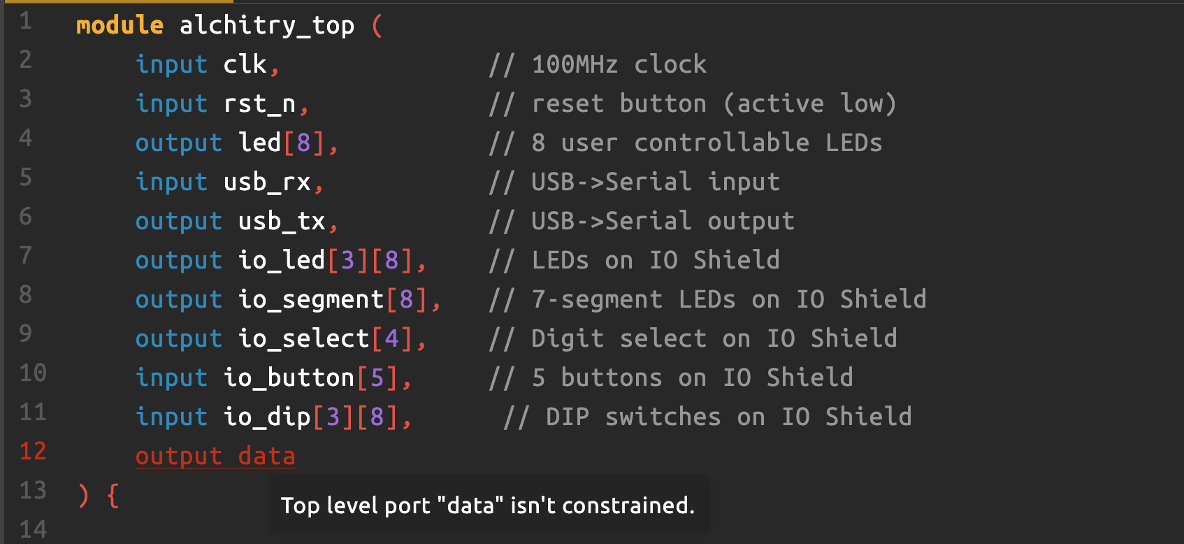
This is Alchitry telling you that: “You said you wanted an output called data, but you never told me which physical pins to use on the FPGA!”. Edit your constraint file to add the corresponding pin. If you don’t know what constraint file means, give this guide a read.
7 Segment / LED does not light up
Test Whether Hardware Works
You need to first test if your hardware is not damaged by connecting it to VDD and ground on a breadboard with resistor (any resistor is better than nothing, just pick one).
+---------------------- Breadboard ------------------------+
|                                                          |
|  VDD (3.3V or 5V)   GND                                  |
|     |               |                                    |
|     |               |                                    |
|     |               |                                    |
|     |               |                                    |
|     |               |                                    |
|     +--->|──[ R ]───+                                    |
|          LED     330Ω–1kΩ                                |
|                                                          |
|       ↳ Long leg (anode, +) goes to VDD via resistor     |
|       ↳ Short leg (cathode, –) goes to GND               |
+----------------------------------------------------------+
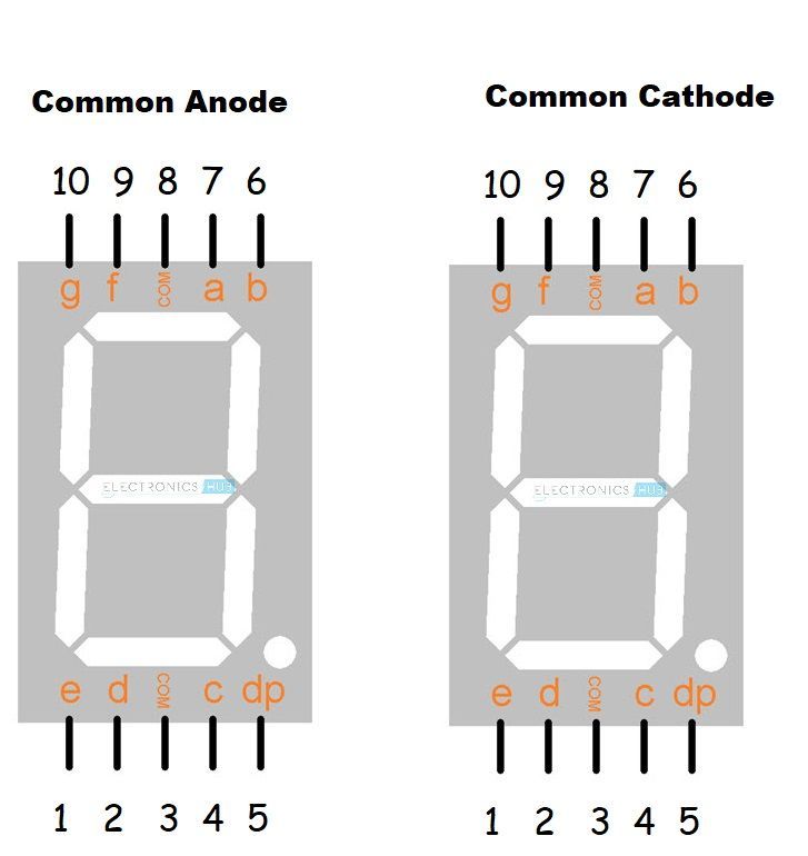
You can also use this method to test individual segments of a 7-segment display, one at a time:
- For common cathode, connect the common pin to GND (segment pins to VDD).
- For common anode, connect the common pin to VDD (segment pins to GND).
This test also helps you double confirm the function of each pin on your 7segment.
Test whether GPIO port on FPGA outputs signal properly
Create a project that drives logic high (1) to every pin you want to use. Then connect each GPIO to an LED + Resistor one at a time.
FPGA GPIO pin ───[ 330Ω ]───>│─── GND
                           LED
If the LED lights up, you know that pin works fine.
Test Static Output
Once the previous two tests are passed and you know the issue is not the hardware nor the GPIO pins, then the issue must be either your pinout or your code or both. Before you start debugging, double check your knowledge by outputting a static value, e.g: turning all LEDs blue, or displaying a fixed digit on your 7segment.
This ensures that your pinouts are correct. Once you are able to output a static value, you can be sure that your hardware, GPIO pins, and knowledge on how to drive the output works fine. This means that the issue is in your code. At this point, you might want to spend some time re-implementing certain logic.
Test Dynamic Output
If you reach this step, it means that there’s certain flaws in your HDL code. You may want to now display dynamic values to your 7 segment (not your project!). One simple idea is to:
- Create a
dffto store binary values from yourio_dipwhenever you press anio_button - This
dffis read bybin_to_decmodule (if using 7 segment) - The output of
bin_to_decmodule drives both the internal 7segment and external 7segment - Check if the numbers you set from
io_dipis displayed on the 7segment - If you are just using plain LEDs, check if the LEDs now show the pattern stored in your
dff - For ease of debugging, also output the content of the
dffonio_led
Using io_top LEDs, dip switches, and buttons ensure that you have a good source of truth, without having to care about wiring connections or pinouts.
Code Works on Simulation but not on Hardware: Outputs flickering, Buttons unstable
Ensure pulldown Constraints
If you observe your code goes haywire whenever you hover on io_button on the physical FPGA, it is likely that you did not utilise the pulldown constraints. Consult this handout on how to fix it.
Connect Everything to a Common Ground
If you are powering your LED matrix, 7-segment display, or any external components using a battery or external power supply, you must connect the ground (GND) of that power source to the FPGA board’s ground.
Why?
Digital signals (like HIGH or LOW) are measured relative to ground. Without a shared ground, the FPGA and external circuit don’t agree on what “0V” means. This can cause unpredictable behavior, no response from the display or potential hardware damage.
Bottomline: always connect the external GND to the FPGA GND pin when using external power.
Failed to meet timing constraint
If your project fails timing, that means your design logic is too slow to keep up with the 100 MHz clock (i.e., 10 ns per cycle). Even if Vivado compiles it, the actual hardware may behave unpredictably. You should lower the clock frequency in the constraint file (e.g., set to 10 MHz) so Vivado checks for more relaxed timing.
But remember: the onboard clock is still 100 MHz. You must manually slow your logic (e.g., FSM or output updates) to match this by adding delay logic (like a clock divider). For example: delay each FSM state by 10 times using a counter, so your effective FSM cycle is 1 per microsecond instead of 1 per 10 ns. Give this page a read to find out how.
Do not attempt to use a project that fails the timing constraint. It might output unpredictable and non-deterministic behavior.
Code Does not Work on Simulation but no Error Reported
The issue might be with your FSM or datapath connection. In order to find out, you need to build a debug infrastructure. Consult the next section.
Code Works on Simulation but not on Hardware: FSM does not go to expected state
This is the hardest bug to fix. It is likely that you encounter timing issues at this point because simulation does not consider timings.
In order to begin debugging, you need to write some kind of debug infrastructure. Ideally, you want to have an FSM that:
- Can be advanced by a button click state by state instead of letting it run, but this feature can be easily disabled later on (for final build)
- Can output all kinds of important signals to
io_led, such as alu’s output, asel/bsel output, wdsel output, or regfile read data output in your 1D project
Remove any Division
Remove code that uses division /. Do not use expressions like a / b where b is not a power of 2.
Division in hardware is complex: it requires a divider circuit, which is large, slow, and significantly more complicated than an adder or shifter.
Most hardware division uses restoring or non-restoring algorithms, or iterative subtraction, which take multiple clock cycles. This introduces sequential logic into your ALU, instead of keeping it purely combinational. As a result, it can mess up your timing, increase your critical path delay, and make synthesis and debugging harder.
If you need to divide by a power of 2, use right shifts instead:
a >> nis equivalent to \(\frac{a}{2^n}\), and is synthesized efficiently with simple wiring logic.
In short: stick to shifts for division, unless you really know what you’re doing and have the extra cycles (literally). Once you have done this, recompile the project and test.
Ensure Timing Constraint is Met
Ensure you do not see any warning as such when you compile your project:
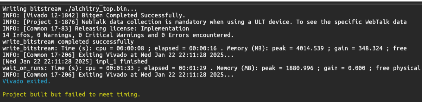
If you do, give this lab a read to fix it first (by slowing the clock or slowing the FSM).
Manually Advancing the FSM
If none of the above works, you should debug your FSM state-by-state.
This part is crucial for debugging, because it helps you narrow down the problematic states. You can start by using one of the buttons, e.g: io_button[0] as an “advance” or “next” button. As usual, pass it through a button conditioner and edge detector:
    // in alchitry_top
    button_conditioner advance_button_conditioner(#CLK_FREQ(CLK_FREQ), .in(io_button[0]))
    edge_detector advance_button_edge(#RISE(1), #FALL(0), .in(advance_button_conditioner.out))

    // if instantiated in other module, simply pass advance_button_edge.out to it
    game_cu(
        // other port connection
        .fsm_clock(advance_button_edge.out)
    )
Then receive the button edge input in your module that contains the game FSM (e.g; the Control Unit module). You then should declare a sig to post-process this button press, and prepare a debug dff as well as debug_out port in this module. The job of the debug output is to indicate which state you are currently at.
module game_cu (
    input clk,  // clock
    input rst,  // reset
    input fsm_clock,
    // other ports
    ...

    output state_debug_out[8]
){
    // module instantiation
    // other modules here

    dff debug[8](.clk(clk), .rst(rst), #INIT(0))
    sig advance

    always{
        advance = fsm_clock
        debug.d = debug.q
        state_debug_out = debug.q

        // other code
    }
}
In the FSM implementation, set debug.d into different combination depending on the states we are in, and set the FSM to go to next state only when advance == 1. For instance:
    States.SET_POINTS:
        alufn = b011010 // "A"
        asel = b10 // Decimal 1
        wdsel = b000 // Route ALU's output
        regfile_wa = d4
        if(advance){
            regfile_we = 1
            game_fsm.d = States.RESET_TIMER
        }
        debug.d = 8d2 // unique debug signal when we are at SET_POINTS

    States.RESET_TIMER:

        alufn = b011010 // "A"
        asel = b11 // Decimal 25
        wdsel = b000 // Route ALU's output

        regfile_wa = d1
        if(advance){
            regfile_we = 1
            game_fsm.d = States.SPAWN_MOLE
        }
        debug.d = 8d4 // unique debug signal when we are at `RESET_TIMER`
It is important that regfile_we or any write enable signal is put under the advance clause as shown above. This is because we do not want our regfile to be repeatedly overwritten.
The following state will not work as expected if regfile_we is put outside the if block:
    States.UPDATE_SCORE:
        alufn = b000000 //  +
        regfile_ra1 = d3 // currentScore dff
        regfile_ra2 = d4 // scoreToAdd dff
        asel = b00 // select rd1
        bsel = b00 // select rd2
        regfile_we = 1 // WRONG! we should NOT be outside advance
        regfile_wa = d3 // currentScore dff
        if(advance){
            game_fsm.d = States.RESET_TIMER

        }
        debug.d = 8d8
Since advance will only be 1 if we press the io_button, then we will loop at this state for millions of loops before we press the advance button. We will end up repeatedly adding the content of currentScore dff with scoreToAdd dff for a million times. Your final score will not reflect the true value at this state.
Instead, do this:
    States.UPDATE_SCORE:
        alufn = b000000 //  +
        regfile_ra1 = d3 // currentScore dff
        regfile_ra2 = d4 // scoreToAdd dff
        asel = b00 // select rd1
        bsel = b00 // select rd2
        regfile_wa = d3 // currentScore dff
        if(advance){
            regfile_we = 1 // CORRECT! write ONCE only when advance is 1
            game_fsm.d = States.RESET_TIMER
        }
        debug.d = 8d8
This ensured that we are only writing to the regfile once, that is in the clock cycle where advance is 1.
With this setup, you should be able to now manually advance your FSM with a click of a button.
The IDLE State: leave as-is
Howevere you cannot do this in the state where you are waiting for another button edge press, or some slow clock edge. One example would be the IDLE state or some kind of WAIT_INPUT state. For instance, do not add the advance button functionality on either of these states:
            States.START:
                if (start_button_edge_pressed) {
                    game_fsm.d = States.INITIALIZE
                }

                else {
                    game_fsm.d = States.START
                }
                debug.d = 8d1

            States.IDLE: // wait for input
                debug.d = 8d5
                if (decrease_timer) {
                    game_fsm.d = States.CHECK_TIMER
                }

                else if (button_p1_edge_pressed) {
                    regfile_we = 1
                    regfile_wa = d2
                    wdsel_out = b010
                    game_fsm.d = States.REGISTER_P1_MOVE
                }

                else if (button_p2_edge_pressed) {
                    regfile_we = 1
                    regfile_wa = d3
                    wdsel_out = b010
                    game_fsm.d = States.REGISTER_P2_MOVE
                }

                else {
                    game_fsm.d = States.IDLE
                }
This is because you won’t be able to press two buttons exactly at the same clock cycle. If you do the START state as such, you might never be able to go to the INITIALIZE state very easily.
    States.START:
        if (start_button_edge_pressed) {
            if (advance) game_fsm.d = States.INITIALIZE // very unlikely to happen
        }

        else {
            game_fsm.d = States.START
        }
        debug.d = 8d1
Display All Crucial Information
Once you are able to make your FSM advance manually using button presses, you need to create an infrastructure in alchitry_top so that you can inspect all sort of signal values in that particular states. You can utilise io_dip for this, just like how we set the output to debug Lab 4: Beta. You should inspect all kinds of crucial signals: the output of asel/bsel, the output of wdsel, output of ALU, output of important dffs, etc.
For instance, your datapath module should output the following (and more):
module game_datapath (
    input clk,  // clock
    input rst,  // reset

    // input and output of datapath

    // debug output
    output p1_score_dff_debug[16],
    output p2_score_dff_debug[16],
    output rd1_out_debug[16],
    output rd2_out_debug[16],
    output current_timer_dff_debug[16],
    output alu_out_debug[16],
    output wdsel_out_debug[16],
    output bsel_out_debug[16],
    output asel_out_debug[16],
    output control_signals_debug[16], // asel(3) bsel(3) wdsel(3) ra1(3) ra2(3), ignore MSB
    output state_out_debug[16]

) {
 // implementation
}
You would need to create intermediary signals to route it both to output and the corresponding module. For example:
    sig asel_out[32]

    // in always body
        case(control_system.asel){
            b0:
                asel_out = regfile_system.rd1
            b1:
                asel_out = 32d30 // constant 30
            default:
                asel_out = regfile_system.rd1
        }

        // hook it up to the output port
        asel_out_debug = asel_out

        // also connect it to alu
        alu.a = asel_out
Do not do the following:
        // HARD TO DEBUG!
        case(control_system.asel){
            b0:
                alu.a = regfile_system.rd1
            b1:
                alu.a = 32d30 // constant 30
            default:
                alu.a = regfile_system.rd1
        }
Consult Lab 4: Beta code for inspiration.
Then in alchitry_top, utilize the dip switches to show different debug values. For instance:
case (io_dip[0]){

            h00:
                io_led[1:0] = $build(datapath.state_out_debug, 2)
                seg.values = $build(datapath.state_out_debug, 4)
            h01:
                io_led[1:0] = $build(datapath.asel_out_debug, 2)
                seg.values = $build(datapath.asel_out_debug, 4)
            h02:
                io_led[1:0] = $build(datapath.bsel_out_debug, 2)
                 seg.values = $build(datapath.bsel_out_debug, 4)
            h03:
                io_led[1:0] = $build(datapath.wdsel_out_debug, 2)
                seg.values = $build(datapath.wdsel_out_debug, 4)
            h04:
                io_led[1:0] = $build(datapath.alu_out_debug, 2)
                seg.values = $build(datapath.alu_out_debug, 4)
            h05:
                io_led[1:0] = $build(datapath.rd2_out_debug, 2)
                seg.values = $build(datapath.rd2_out_debug, 4)
            ...
           // and so on, for each of debug signal from datapath

    }
Build and Debug
With the debug infrastructure in place, you can safely trace the error both on simulation (if you didn’t use any BRAM) and on the hardware. This will give you a clue whether:
- Are any states problematic? (did not go to the right state in hardware but go to the right state in simulation)
- Is a particular state triggered? (useful to check if simulation does not work either)
Debug: Replace the ALU (Temporarily)
Once you have identified the problematic state, you can temporarily replace your ALU with instructor ALU and see if the problem persists.
Debug: Use Lucid Operators Directly in a State (Temporarily)
In a problematic state, you may try to use Lucid Operators directly such as (assume control unit directly gets RD2 from regfile):
    States.CHECK_PRESS_P1:

        regfile_ra2 = d0 // P1 button press

        if(regfile_rd2_out < 3){ // use lucid operator, bypass ALU
            game_fsm.d = States.INCREASE_SCORE_P1
        }
        else{
            game_fsm.d = States.IDLE // ignore button press
        }
        debug.d = 8d6
Some States (not all) does not Transition as Expected
It is likely that you have violated timing constraints if the code works on simulation but fails on actual FPGA. Give this page a read to either slow down the input clk or slow your FSM while still using the default 100MHz clock.
Display Matrix Does not Work
You need to first ensure that your game logic is solid on both hardware (io top) and simulation. Once you have done this, you might realise that your display matrix did not display what you wanted. The issue might either be in your hardware or your driver.
First, check that your matrix works using instructor’s driver demo (WS2812B or HUB75 style matrix). The code should work as-is without any modification.
If it does not work, then check your connection, or it is likely that your hardware has spoiled. You might need to purchase a backup hardware.
Otherwise, if it works, then you would need to slowly trace your code again and ensure it outputs the right thing. Consider the following infrastructure that highlights separation of concern.
[Datapath] ---> (writes) ---> [Display Buffer] ---> (reads) ---> [Display Driver] ---> [LED Matrix]
Create a Display Buffer
Use a dedicated register (DFF) or memory module (e.g., BRAM, simple_ram, or simple_dual_ram) to act as a display buffer. This module’s only purpose is to store the current screen state, nothing more.
Display Driver: Read-Only Access
The display driver should only read from the display buffer. It should never perform logic or calculations. Think of it as a “dumb” renderer, it simply reads what’s in the buffer and sends it to the display hardware.
Datapath: Write-Only Access
Your logic (Datapath) should only write to the display buffer. All computations happen elsewhere typically in your REGFILE or control logic. The display buffer just holds the final output to be shown.
This separation of concerns makes your design easier to debug and reason about and avoids conflicts between components trying to read/write the same data at the same time.
Summary
These debug strategies generally work to catch any bug with your 50.002 1D project within a reasonable time, but they are not magic tools. Debugging HDL requires patience and discipline. Sometimes, it might be easier to remake the project from scratch and does incremental test (both on simulator and hardware). Good luck!