 50.002 CS
- Overview
- Download BSIM
- Instruction Cycles
- Detailed Anatomy of the \(\beta\) CPU
- Beta Datapaths
- Basic Operation Datapath
- Memory Access Datapath
- Control Transfer Datapath
- More about RESET
- How Does CPU Interpret Signed vs Unsigned Numbers?
- CPU Benchmarking
- Summary
- Next Time
50.002 Computation Structures
Information Systems Technology and Design
Singapore University of Technology and Design
Building the \(\beta\) CPU
You can find the lecture video here. You can also click on each header to bring you to the section of the video covering the subtopic.
Detailed Learning Objectives
- Explain the Relationship Between Control Logic and CPU Instruction Handling
- Explain how the Control Logic unit decodes the OPCODE of instructions and outputs appropriate control signals to manipulate the datapath for executing various instructions.
- Implement the datapath for \(\beta\) ISA
- Examine the Instruction Fetch and Decode Process
- Describe how the CPU fetches and decodes instructions during each clock cycle, focusing on the computation of instruction addresses and the decoding of OPCODEs.
- Analyze the Detailed Anatomy of the \(\beta\) CPU
- Design the components of the \(\beta\) CPU, including the Program Counter (PC), Register Files (REGFILE), Arithmetic Logic Unit (ALU), and Control Unit (CU), and their interconnections.
- Explain Memory Interaction in the CPU
- Investigate how instructions interact with memory, specifically how data is loaded and stored between the CPU’s registers and the physical memory unit.
- Explain the Control Transfer in CPU Operations
- Design instructions that involve control transfer such as conditional branches and jumps, and understand how they modify the flow of execution within the CPU.
- Describe the \(\beta\) Instruction Set
- Describe all instructions under the \(\beta\) ISA, their formats, and how they are executed within the CPU’s datapath.
- Assess the Role of the Control Unit in Instruction Execution
- Identify how the Control Unit’s signals direct the CPU’s datapath to execute instructions correctly based on the decoded instruction type.
- Assess CPU Performance with Benchmarks
- Evaluate CPU performance using metrics such as MIPS (Million Instructions Per Second) and understand the implications of CPI (Clocks Per Instruction) on performance assessment.
These objectives help students grasp the intricate details of how a CPU interprets and executes instructions based on a predefined instruction set architecture, using the \(\beta\) CPU as a model system.
Overview
In the previous chapter, we were introduced to the \(\beta\) ISA, a CPU blueprint that specifies what instructions the CPU can process, how it interacts with the memory unit, the basic CPU components, instruction formats, and many more.
In this chapter, we will study how each of the 32 \(\beta\) instructions is supposed to work, and how the \(\beta\) CPU (an implementation of the \(\beta\) ISA) is able to compute each and every one of them by reprogramming its datapath without physically changing its hardware.
The key is to have a proper Control Logic unit that is able to decode current instruction’s OPCODE and give out the correct control signals (PCSEL, RA2SEL, ASEL, etc) to reprogram the datapath. The complete truth table of the control logic unit is as shown below,

This unit can be easily implemented using a read only memory.
We will go through the function of each instruction and understand how the given \(\beta\) datapath is able to execute the instruction properly by producing appropriate control signals as shown above.
Download BSIM
BSIM is a Beta simulator for the 50.002 Beta CPU. You can run Beta instructions there and observe the output in action. Please download it from here before proceeding.
Instruction Cycles
At each clock cycle, the CPU has to first fetch the current instruction from the Memory and decode its OPCODE. This instruction tells the CPU what to do for this clock cycle.
Instruction Fetch
The first thing a CPU must do is to compute the address (ia[31:0]) of the instruction to execute next, and then fetch (read) them (id[31:0]) from the Physical Memory Unit (RAM). When we write programs in high-level languages, its compiler or interpreter will translate them into machine instructions that are specific to the CPU’s ISA. The control unit will know what control signals to produce and which signals need to be routed where for each type of instruction.
Starting Address Assumption
As of now, you always assume that the content of the PC register is always initially zero (32-bit of zeroes), and that the first line of your program instruction is always put at memory address zero (
0x00000000). That means the first instruction to your program (first line of code) must be placed in the Memory in address 0.
Instruction Decoding
When the CPU has an instruction, it needs to figure out (decode) specifically what type of instruction it is. Each instruction will have a certain set of bits called the OPCODE that tells the CPU how to interpret it. In the \(\beta\) ISA, the OPCODE can be found in the 6 most significant bits of the 32-bits \(\beta\) instruction. This OPCODE is given as an input to the Control Unit, and the Control Unit will compute the appropriate control signals to program the datapath.
This decoding step depends on how complex the ISA is. RISC-based computers (e.g: the \(\beta\) ISA) has a smaller number of instructions (a few dozens) of the same length, while x86-based computers have thousands of differing lengths. In either architecture, we can group their instructions into these three families in general?
- Memory Access: anything regarding loading and storing of data between the REGFILE (CPU internal storage) and the Memory Unit. No other computation is performed.
- Arithmetic: anything that requires computation using the ALU, and inputs are taken from the REGFILE.
- Branch instructions: anything pertaining to changing the value of PC Register to load instructions in different Memory Address, (conditional) based on a content of a specific register in the REGFILE.
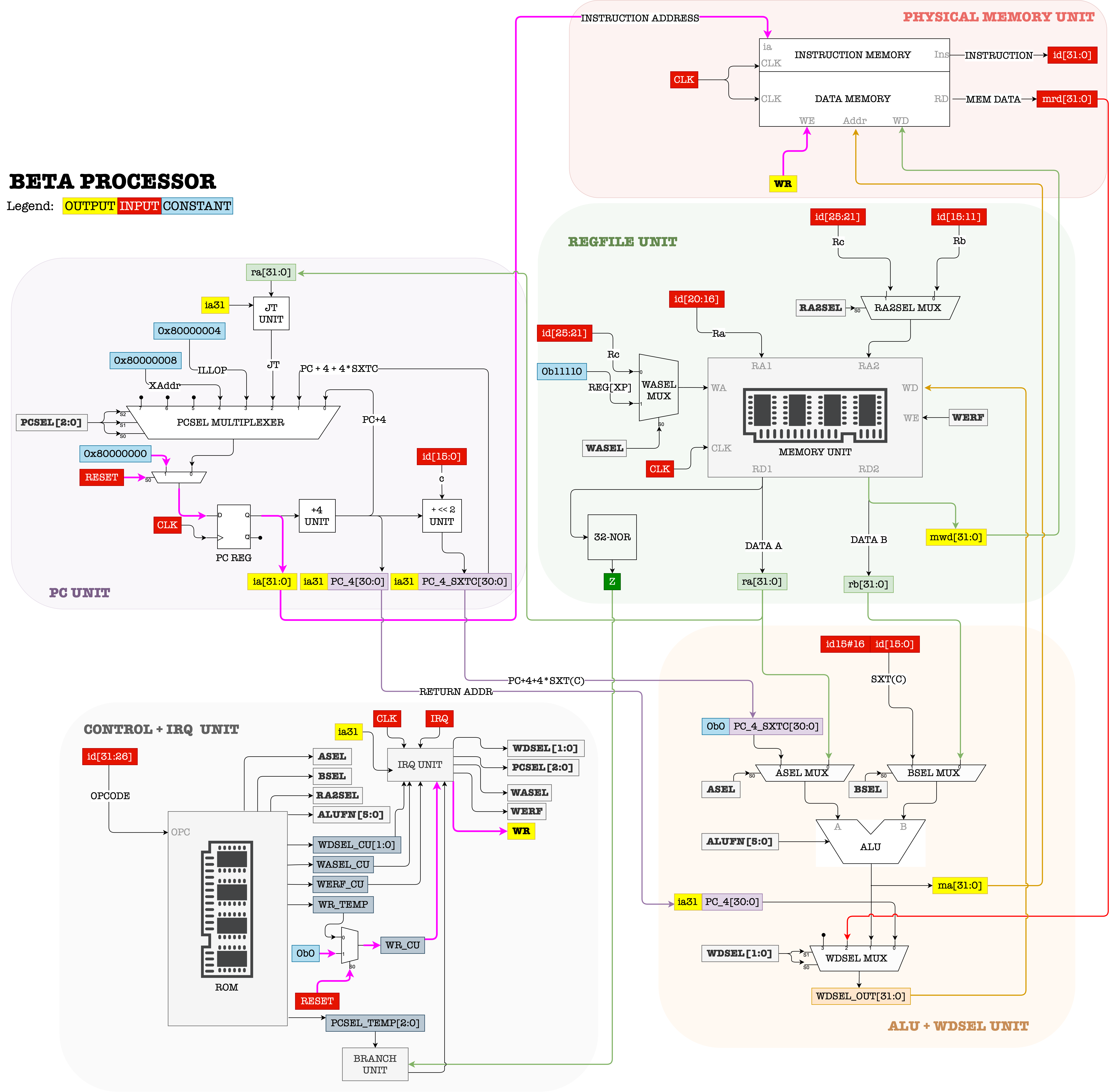
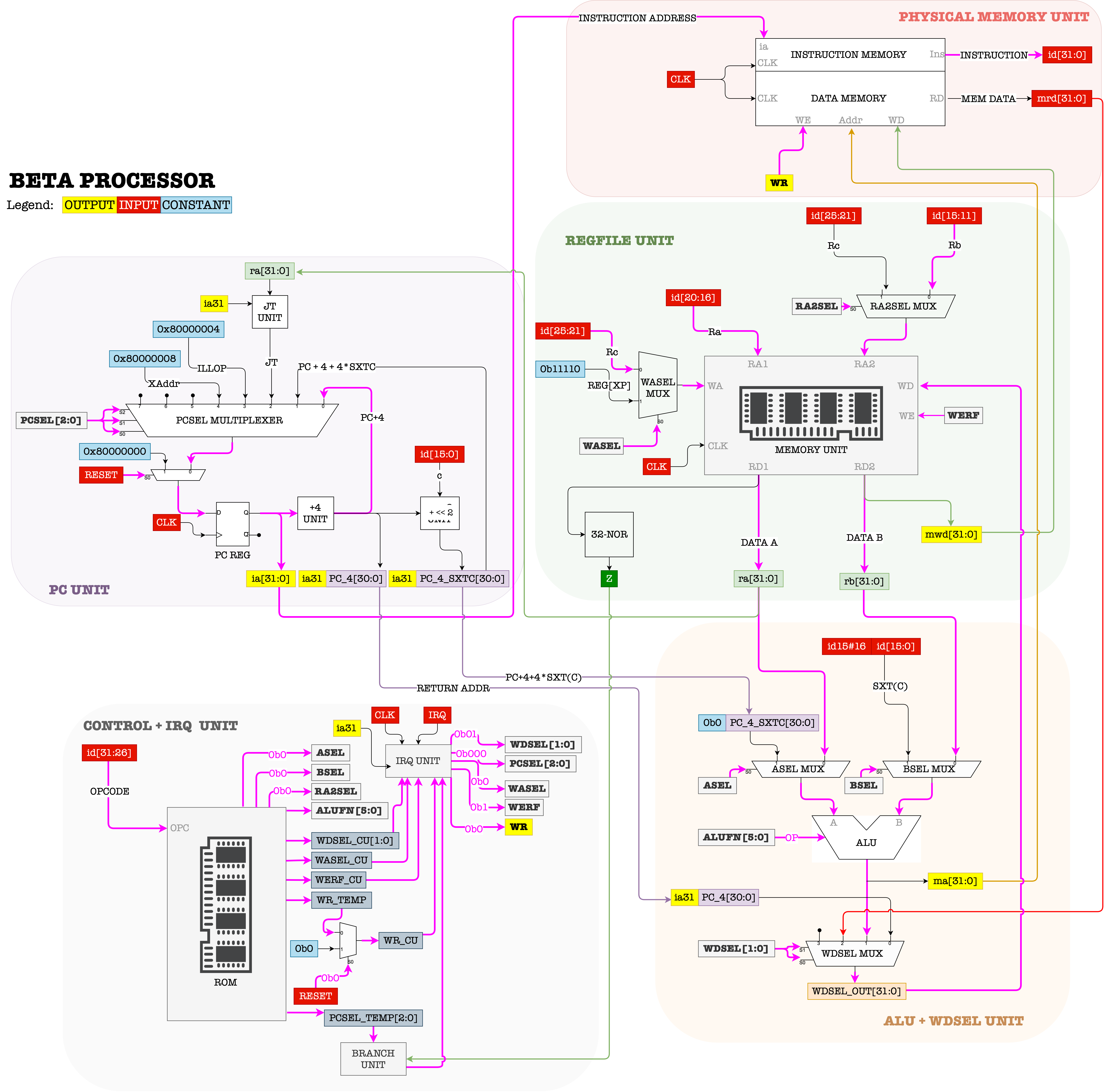
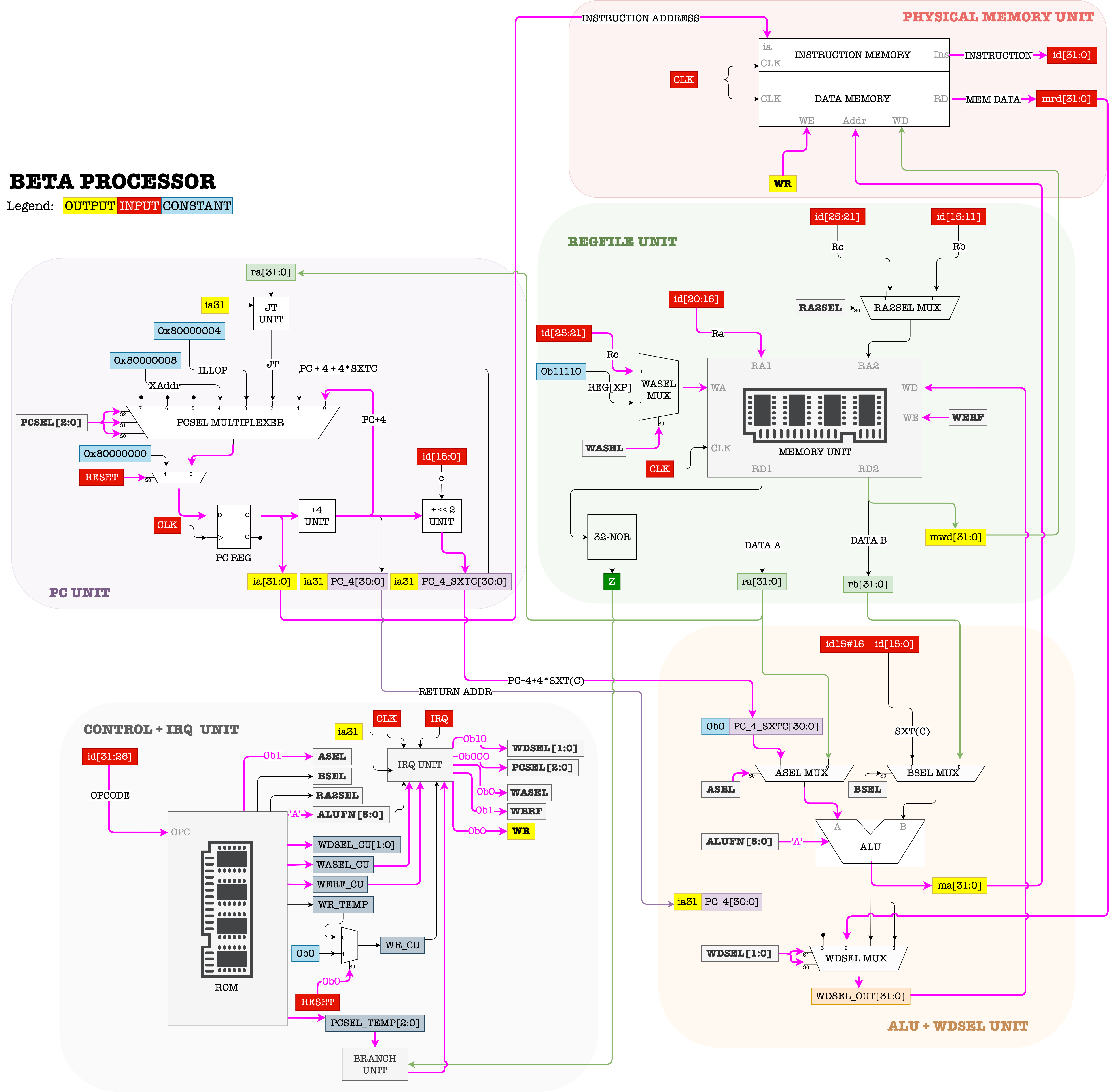
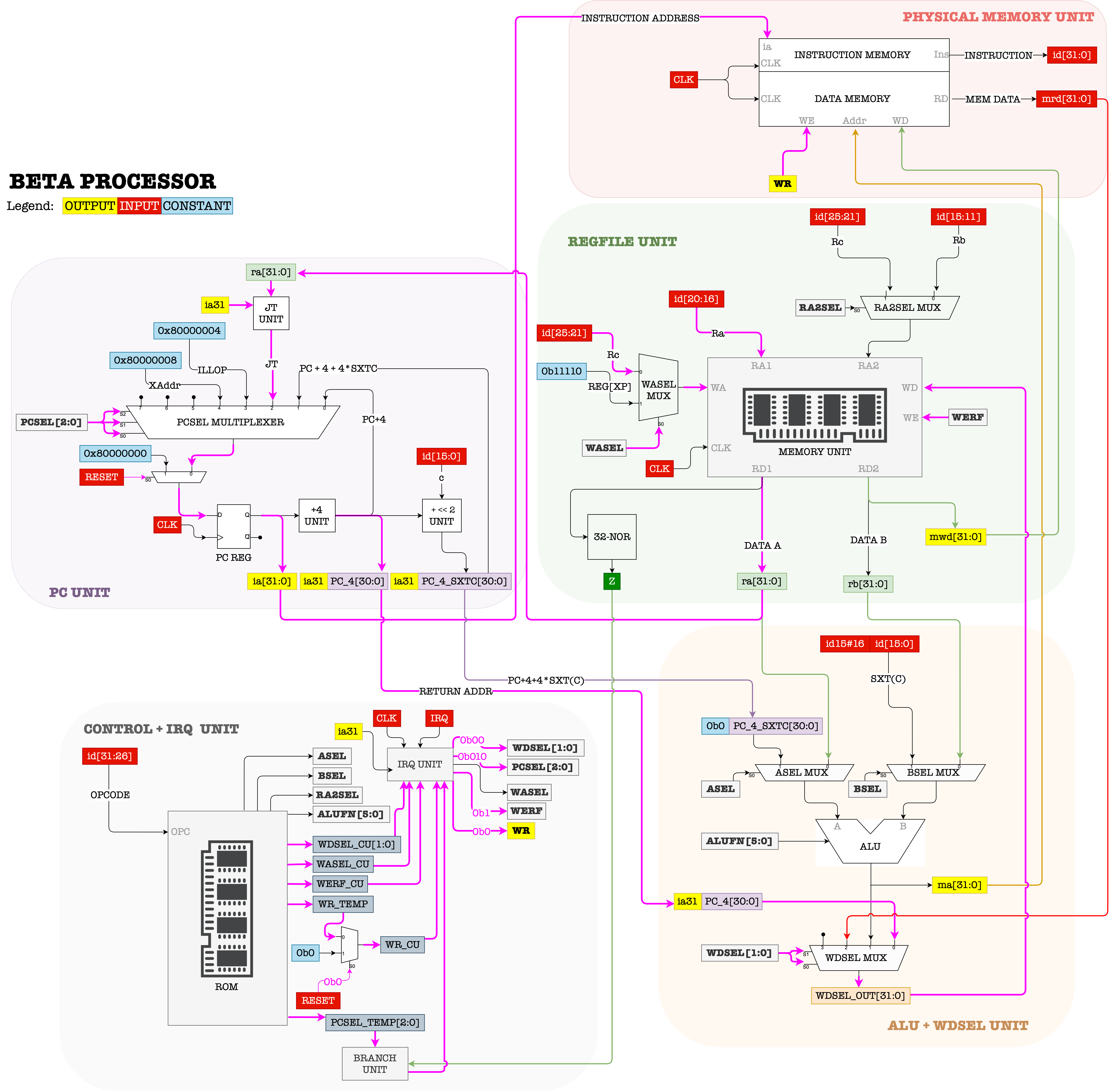
Detailed Anatomy of the \(\beta\) CPU
The \(\beta\) CPU is comprised of the following standard parts that typically make up a CPU:
- PC (program counter),
- REGFILE (register file),
- ALU (arithmetic logic unit), and
- CU (control unit).
Program Counter and Physical Memory Unit
The PC is a 32-bit register (i.e: a set of 32 1-bit registers). Its job is to store the address of the current instruction that is executed. For now, we can safely assume that the initial content of the PC REG is always 0x0 (32 bits).
The datapath of the components involving the PC and the Physical Memory is shown in the figure below:
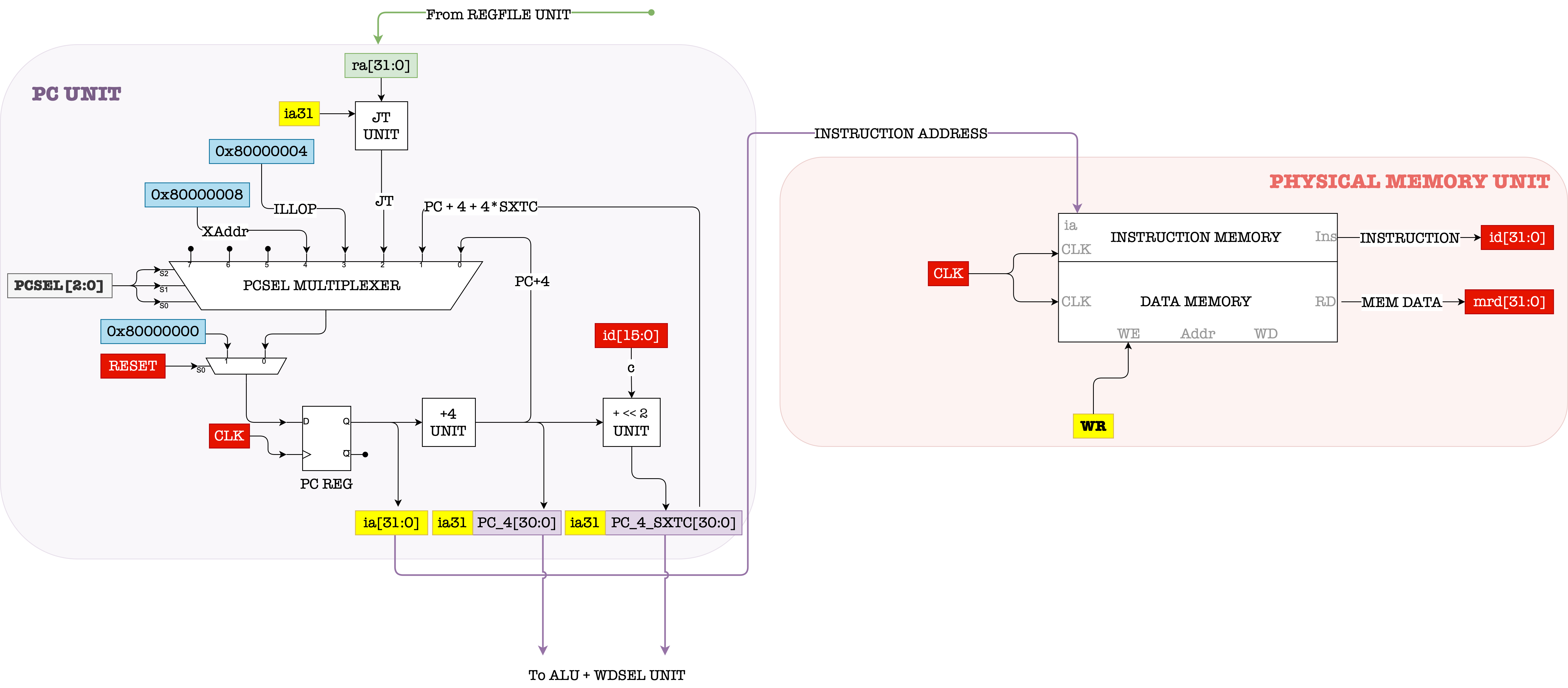
The memory unit is neatly segmented into instruction memory and data memory for the sake of learning and simplicity. In reality, this might not always be the case. Your operating system will do the memory management for you and decide where in the physical memory each process should reside and run.
Two important things happened at the same time at every CPU clock cycle:
- The output of the PC Register is connected to the
iaport (the input address port) of the Memory Unit (RAM or Physical Memory), hence the Memory Unit will produce the content of that address through theIns(instruction) port. - The output of the PC REG will also be added by 4.
- If
PCSEL=0andRESET=0, this value (old PC + 4) will enter the PC REG in the next clock cycle. This will cause the PC to supply the address of the subsequent instruction word in the next clock cycle. - If
PCSEL!=0andRESET=0, then the value in the PC REG will be equivalent to either of the inputs to the PCSEL MUX (depending on whatPCSELvalue is).
- If
RESET
If RESET=1 then the value of the PC REG in the next cycle will be equivalent to RESET. We will learn what RESET is in the later weeks but in short, if RESET=1, then the value in the PC REG will will be set to 0x80000000 in the next clock cycle instead of being increased by 4 or whichever other address that the supposed current instruction should compute.
You will learn in the Virtual Machine chapter on why the MSB of RESET is 1 instead of 0, but for now you can take its purpose as simply resetting the machine and eventually putting content of PC REG content back to 0 (restarting the program).
Setting
PC=RESETmeans that we will execute whatever instruction that resides at0x80000000in the next cycle. The instruction that resides in theRESETaddress is called the reset handler. It is usually a standard routine to restart your computer/devices.
Register Files
The REGFILE in \(\beta\) ISA is the CPU’s internal storage unit that is comprised of 32 sets of 32-bit registers, denoted as \(R_0, R_1, ...., R_{31}\). Each register is addressable in 5 bits. For example: 00000 is the address of \(R_0\), 00001 is the address of \(R_1\), 00010 is the address of \(R_2\), and so on.
Remember, a 32-bit register simply means a set of 32 1-bit registers
The figure below shows the anatomy of \(\beta\) REGFILE component:
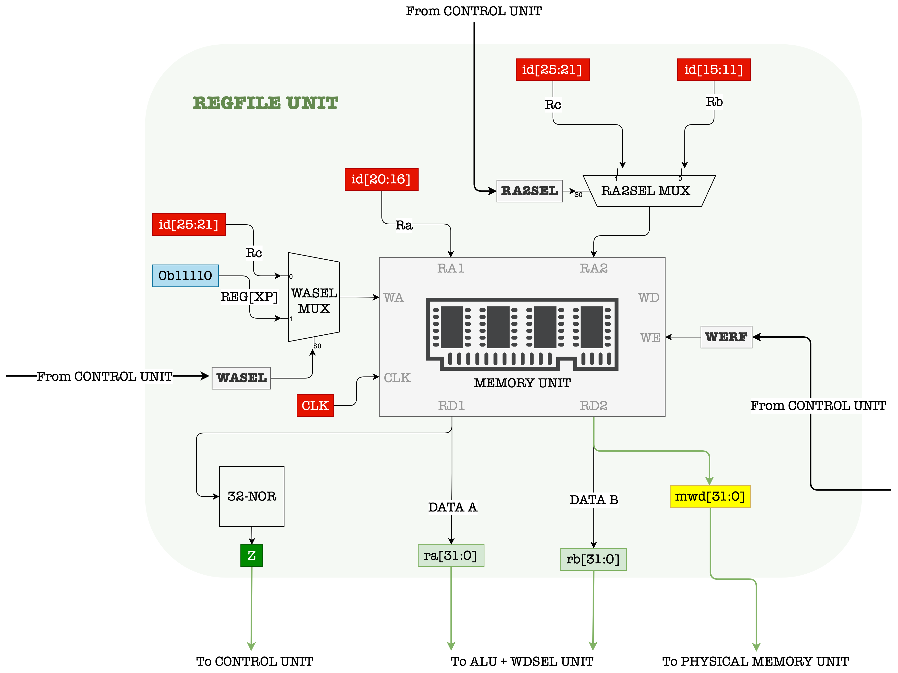
It has two combinational read ports: RD1 and RD2, and one clocked/sequential write port: WD.
We can simultaneously (at the same clock cycle) read the contents of two selected registers, addressable in 5 bits denoted as Ra and Rb, :
- The 5-bit address
Rais supplied through portRA1 - The 5-bit address
Rbis supplied throughRA2
We can also write data supplied at the WD port to any of the registers in the REGFILE:
- In order to write, a valid
1must be supplied at theWEport - The address of the register to write into is determined by the 5-bit input supplied at the
WAport.
The Write Enable Signal
Recall that a register / D Flip-Flop sort of captures a NEW input value at each CLK rise, and is able to maintain that stable value for the period of the CLK.
However, in practice, we might not want our register to “capture” new input all the time, but only on certain moments. Therefore, there exist a WE signal such that:
- When it’s value is
1, the register “captures” and stores the current input in in it’sMEMORYmode. - Otherwise, the register will ignore the input and will output the last stored value regardless of the CLK edge.
Detailed Anatomy of the REGFILE
To understand how the Write Enable WE signal works more clearly, we need to dive deeper into the inner circuitry of the REGFILE. The figure below shows a more detailed anatomy of the REGFILE unit.
The Special Register
R31R31’s content is always
0x00000000, regardless of what values are written to it. Therefore it is not a regular register like the other 30 registers in the REGFILE. It is simply giving out0x00000000as output when RA1 or RA2 is 11111, which is illustrated as the 0 on the leftmost part of each read MUXes.
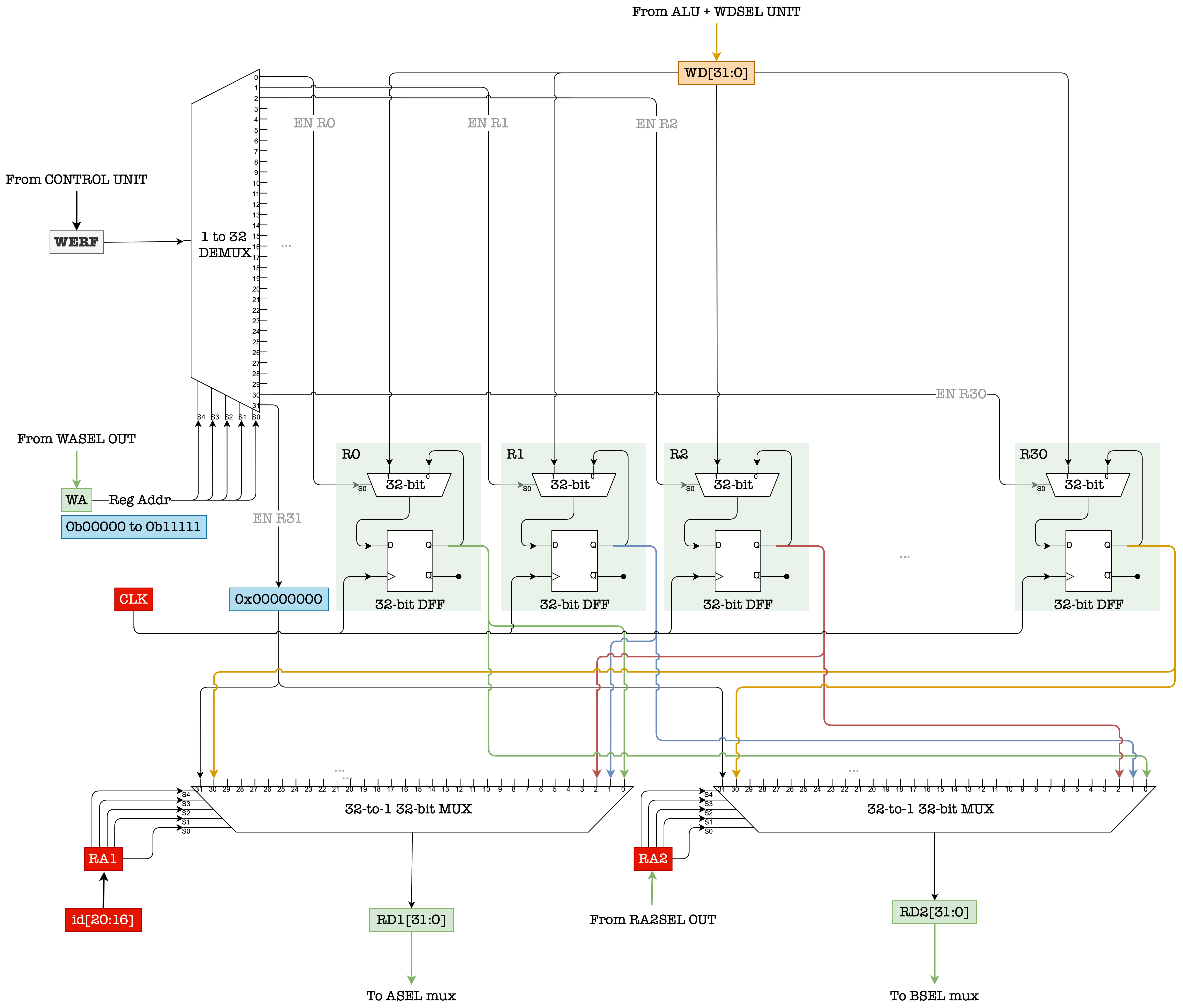
The WE signal is fed into a 1-to-32 demultiplexer unit. The WA signal is the selector of this deMUX. As a result, only 1 out of the 32 outputs of the deMUX will follow exactly the value of WE. The outputs of the deMUX is used as a selector (EN port) to each of the 2-to-1 32-bit multiplexer connected to each 32-bit register.
Although not drawn (to not clutter the figure further), all the registers are synchronized with the same CLK.
The Static and Dynamic Discipline of the REGFILE
As mentioned above, the REGFILE unit has 2 combinational read ports that is made up by the two large 32-to-1 32-bit multiplexers drawn at the bottom of the figure. We can supply two read addresses: RA1 and RA2. They are the selector signals of these two multiplexers. Therefore the time taken to produce valid output (32-bit) data at RD1 and RD2 is at least the \(t_{pd}\) of the multiplexer and \(t_{pd}\) of the DFFs depending on when exactly the addresses become valid.
This unit also have 1 sequential write port. The write data is always supplied at WD. When the EN signal of a target register is a valid 1, we need to wait until the nearest CLK rise edge in order for WD to be reflected at the Q port of that register.
In register transfer language, the content of register with address A is often denoted as : Reg[A]
The timing diagram for read and write is shown below. Please take some time to study them:

Notice how the new data denoted as new Reg[A] supplied at port WD (to be written onto Reg[A]) must fulfill both \(t_S\) and \(t_h\) requirement of the hardware.
Register Content (32 bits) vs Register Address (5 bits)
The CONTENT of a Register
Rain a REGFILE is distinct from the ADDRESS of RegisterRain the REGFILE. For instance, you can store the value0xDEADBEEFin RegisterR3. The address of this register is 3 (0b00011) but the content is0xDEADBEEF.
Control Logic Unit
The heart of the control logic unit (CU) is a combinational logic device that receives 6-bit OPCODE signal, 1-bit z signal, 1-bit RESET signal, and 1-bit IRQ signal as input. We will discuss about RESET, z and IRQ much later on.
At each CLK cycle, the PC will supply a new 32-bit address to the Memory Unit, and in turn, 32-bit instruction data is produced by the Memory Unit. The first 6 bits of the instruction, called the OPCODE is supplied as an input to the CU.
The CU will then decode the input combination consisted of OPCODE, z, RESET, and IRQ, and produce various control signals as shown in the figure below. In practice, this unit can be made using a ROM.
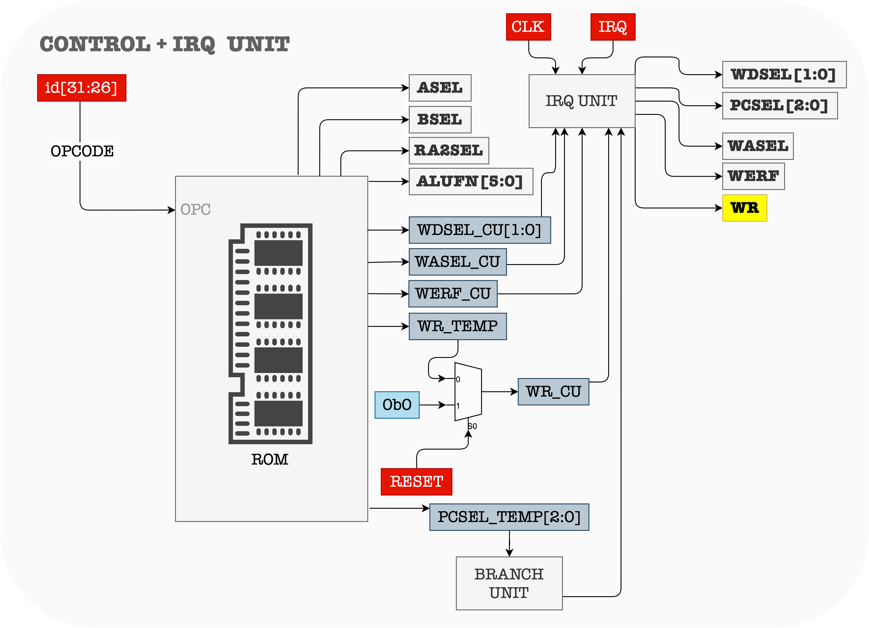
Note that the ALUFN is 6 bits long, PCSEL is 3 bits long, WDSEL is 2 bits long, RA2SEL, BSEL ASEL, WASEL, WR, and WERF (WE to REGFILE) are all 1 bit long. The total number of output bits of the CU is therefore at least 17 bits long
In our Lab however, the output signal of the control unit is 18 bits long. We don’t have to memorise these, as long as we get the main idea.
The IRQ (Interrupt) Signal
Notice the presence of
clkas input into the Control Unit. This is because we need to sample the interrupt signal at the beginning of instruction execution. You may ignore this for now, we will learn more about it in the later weeks. For simplicity, we omit the display of this register unit in the diagrams to explain the datapaths below.
Beta Datapaths
The \(\beta\) datapath can be reprogrammed by setting the appropriate control signals depending on the current instruction’s OPCODE. In general, we can separate the instructions into four categories, and explain the datapath for each:
- The
OPdatapath (Type 1): ADD, SUB, MUL, DIV, SHL, SHR, SRA, CMPEQ, CMPLT, CMPLTE, AND, OR, XOR (13 operations) - The
OPCdatapath (Type 2): ADDC, SUBC, MULC, DIVC, SHLC, SHRC, SRAC, CMPEQC, CMPLTC, CMPLTEC, ANDC, ORC, XORC (13 operations) - Memory access datapath (Type 2): ST, LD, LDR (3 operations)
- Control transfer datapath (Type 2): JMP, BNE, BEQ (3 operations)
Total: 32 operations.
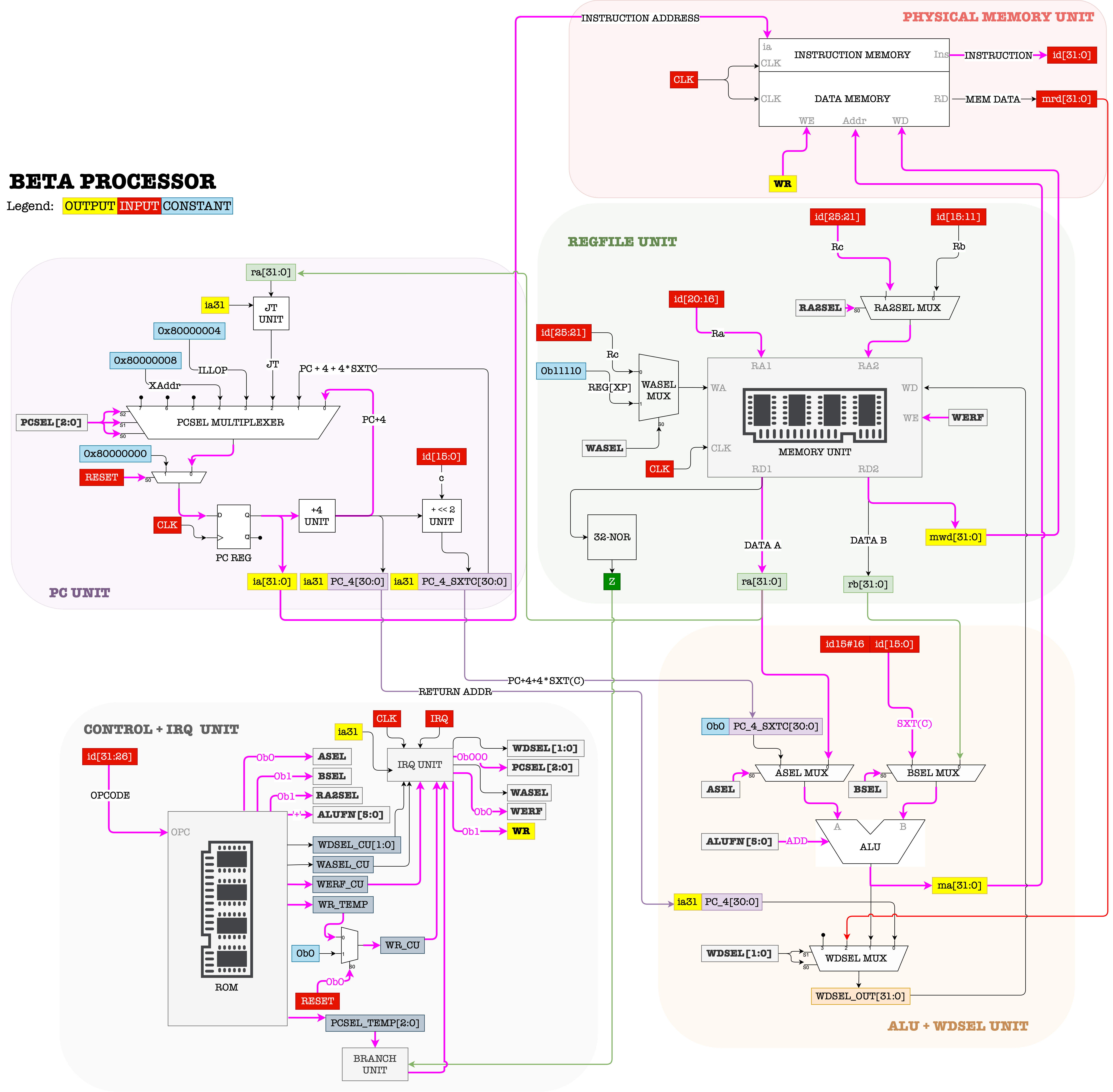
Basic Operation Datapath
OP datapath
Purpose
Perform any logical computations using the ALU. The inputs to the A and B port of the ALU is taken from the contents of any two registers Reg[Ra] and Reg[Rb] from the REGFILE. The output of the ALU is stored as a content of Reg[Rc].
The instructions that fall under OP category are: ADD, SUB, MUL, DIV, AND, OR, XOR, CMPEQ, CMPLT, CMPLE, SHL, SHR, and SRA. Its general format is:

Register Transfer Language
The register transfer language for this instruction is:
PC \(\leftarrow\) PC+4
Reg[Rc] \(\leftarrow\) Reg[Ra] (OP) Reg[Rb]
Assembly Language Format
The corresponding assembly instruction format runnable in BSIM is OP(Ra, Rb, Rc)
Read the \(\beta\) documentation and fully study the functionalities of each instruction.
Datapath
The highlighted lines in pink show how the signals should flow in order for the \(\beta\) to support OP instructions.
Control Signals
ALUFN = F(OP)- This means the
ALUFNsignal for the corresponding operationOP, for example, ifOPCODE = SUBthenALUFN = 010001, and so on.
- This means the
WERF = 1BSEL = 0WDSEL = 01WR = 0RA2SEL = 0PCSEL = 000ASEL = 0WASEL = 0
Think!
Take some time to understand why the value of these control signals must be set this way to support the
OPinstructions.
OPC datapath
Purpose
Perform any logical computations using the ALU (similar to OP above). The OPC (Type 2 instruction) datapath is similar to the OP datapath, except that input to the B port of the ALU must be a constant that comes from c = I[16:0], sign extended to 32-bits. There is no Rb field in Type 2 instruction, only the c-field. The output is stored as a content of Reg[Rc]
The instructions that fall under OPC category are: ADDC, SUBC, MULC, DIVC, ANDC, ORC, XORC, CMPEQC, CMPLTC, CMPLEC, SHLC, SHRC, and SRAC. It’s general format is:

Register Transfer Language
PC \(\leftarrow\) PC+4
Reg[Rc] \(\leftarrow\) Reg[Ra] (OP) SEXT(C)
Again, don’t forget to read \(\beta\) documentation to understand each functionalities.
Assembly Language Format
The corresponding assembly instruction format runnable in BSIM is OPC(Ra, c, Rc)
Datapath
Control Signals
The control signals for OPC instructions are almost identical to OP operations, except that we need to have BSEL = 1.
Sample Code
Try it Yourself!
Try it yourself by running this code step by step on BSIM and observe the datapath to familiarize yourself with how OP and OPC datapath works.
- At each time step, be aware of the value of PC and all Registers.
- Familiarise yourself with how to translate from the assembly language to the 32-bit machine language
.include beta.uasm

ADDC(R31, 5, R0)
SUBC(R31, 3, R1)
MUL(R0, R1, R2)
CMPEQ(R1, R1, R4)
CMPLT(R0, R1, R4)
SHL(R1, R1, R5)
SRAC(R5, 4, R5)
SHRC(R1, 4, R6)
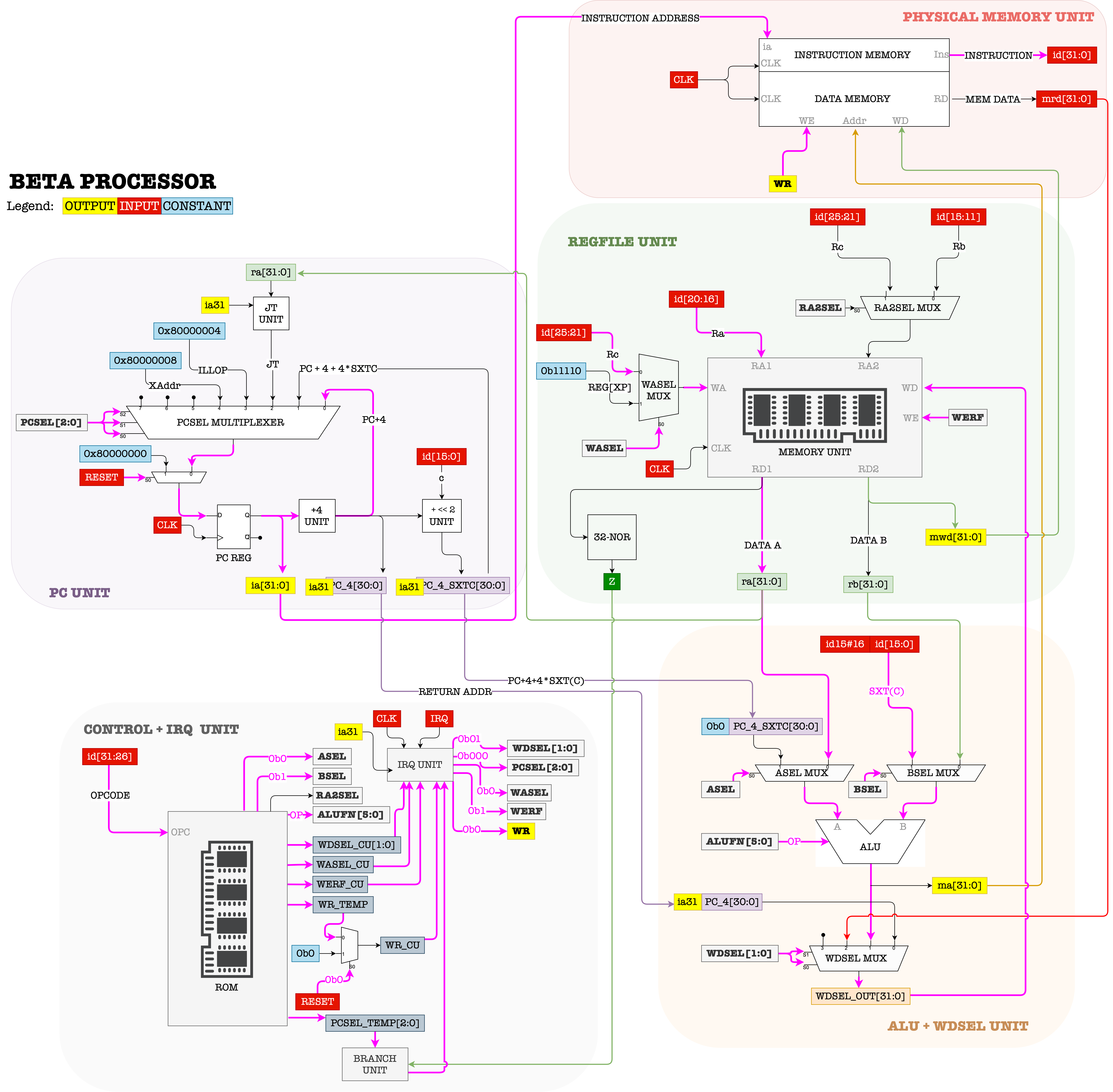
Memory Access Datapath
There are three instructions that involve access to the Memory Unit: LD, LDR and ST. All of them are Type 2 instructions.
LD Datapath
The general format of the LD instruction is:

Purpose
The LD instruction allows the CPU to load one word (32-bit) of data from the Memory Unit and store it to Rc. The effective address (EA) of this data that we are about to Load to the CPU can be computed from adding content of Register Ra and 16 bit signed constant c. The data fetched from memory with this EA is stored as the content of Reg Rc.
Register Transfer Language
PC \(\leftarrow\) PC+4
EA \(\leftarrow\) Reg[Ra] + SEXT(C)
Reg[Rc] \(\leftarrow\) Mem[EA]
Assembly Language Format
The corresponding assembly instruction format runnable in BSIM is LD(Ra, c, Rc)
Datapath
Control Signals
ALUFN = ADD (000000)WERF = 1BSEL = 1WDSEL = 10WR = 0RA2SEL = ----means we don’t care what the value is, since we don’t utilise this datapath involvingRA2SEL
PCSEL = 000ASEL = 0WASEL = 0
LDR datapath
Purpose
The LDR instruction is similar to the LD instruction, except in the method of computing the EA of the data loaded. It computes EA relative to the current address pointed by PC.
The general format of the LDR instruction is:

Register Transfer Language
PC \(\leftarrow\) PC+4
EA \(\leftarrow\) PC+4*SEXT(C)
Reg[Rc] \(\leftarrow\) Mem[EA]
Assembly Language Format
The corresponding assembly instruction format runnable in BSIM is LDR(label, Rc). We give the label (target address) to the assembler, and it auto computes c with the formula: (address_of_label - address_of_current_ins)/4-1
Datapath
Control Signals
ALUFN = 'A' (011010)- The ALU is simply required to be transparent, i.e: “pass” the input at the
Aport through to its output port.
- The ALU is simply required to be transparent, i.e: “pass” the input at the
WERF = 1BSEL = --WDSEL = 10WR = 0RA2SEL = --PCSEL = 000ASEL = 1WASEL = 0
ST datapath
Purpose
The ST instruction does the opposite to what the LD instruction does. It allows the CPU to store contents from one of its REGFILE registers to the Memory Unit. It stores data present in Rc to the Memory Unit.
Similar to how EA is computed for LD, the effective address (EA) of where the data is supposed to be stored is computed using the content of Ra (32-bit) added with c (sign extended to be 32-bit).
The instructions ST and LD/LDR allows the CPU to have access to an expandable memory unit without changing its datapath, although the CPU itself has a limited amount of internal storage in the REGFILE.
The general format of the ST instruction is:

Register Transfer Language
PC \(\leftarrow\) PC+4
EA \(\leftarrow\) Reg[Ra]+SEXT(c)
Mem[EA] \(\leftarrow\) Reg[Rc]
Assembly Language Format
The corresponding assembly instruction format runnable in BSIM is ST(Rc, c, Ra), notice the swapped Rc and Ra position.
Datapath
The control signals therefore must be set to:
ALUFN = 'ADD' (000000)WERF = 0BSEL = 1WDSEL = --WR = 1RA2SEL = 1PCSEL = 000ASEL = 0WASEL = --
Sample Code
Try it yourself!
Try it yourself by running this code step by step on BSIM and observe the datapath to familiarize yourself with how LD, LDR and ST datapath works.
- At each timestep, be aware of the value of PC and all Registers.
- Be aware on the value stored at certain memory locations
- Familiarise yourself with how to translate from the assembly language to the 32-bit machine language using labels and literals
.include beta.uasm

LD(R31, x, R0)
LD(R31, x + 4, R1)
LD(R31, x + 8, R2)
LD(R31, x + 12, R3)
LDR(x, R4)
LDR(x+8, R5)
MUL(R0, R3, R0)
ADD(R1, R1, R1)
ADDC(R31, 12, R6)
ST(R0, x)
ST(R1, x, R6)

x : LONG(15) | this is an array
	LONG(7)
	LONG(9)
	LONG(-1)
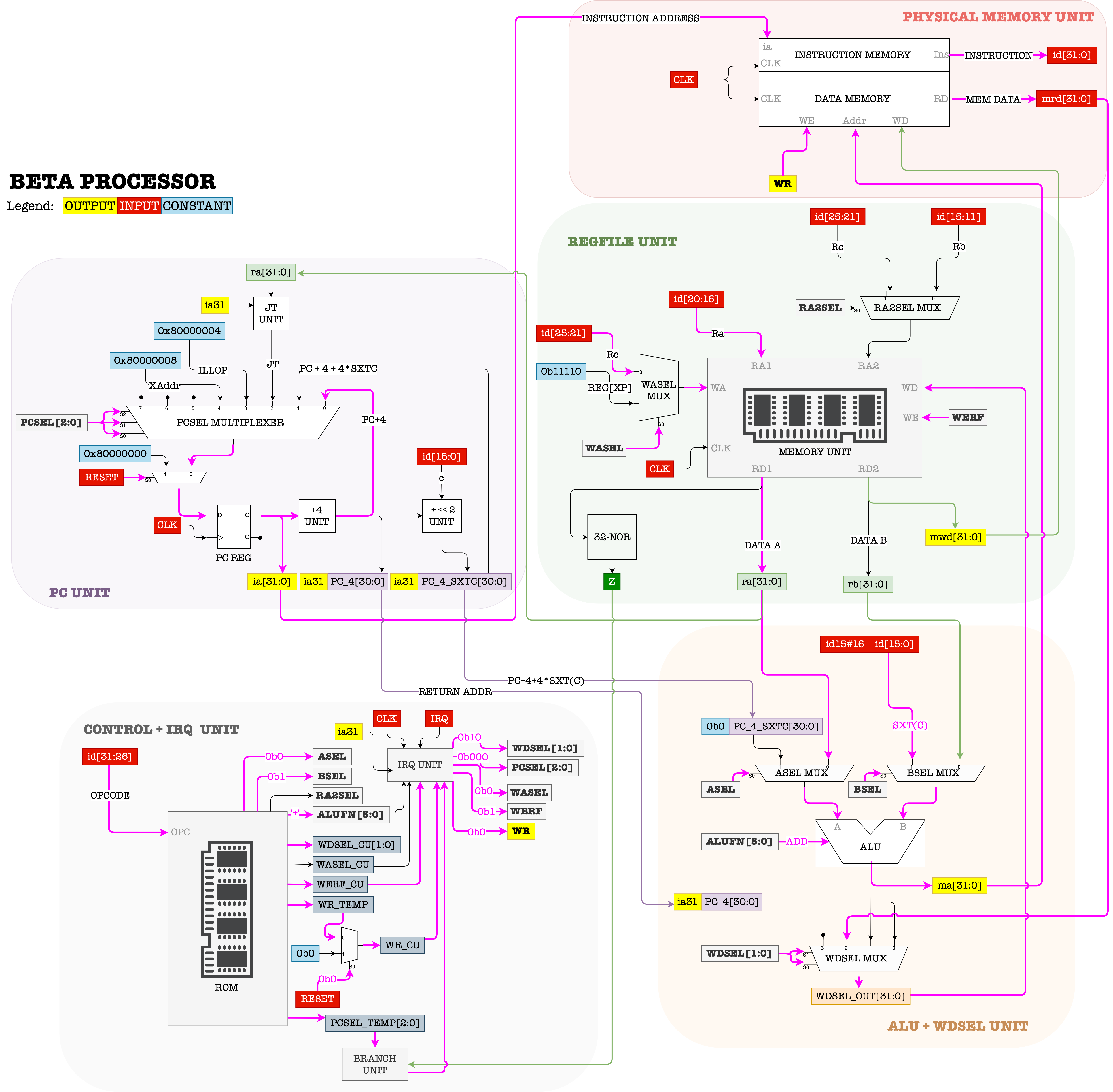
Control Transfer Datapath
So far, we have only seen PC to be advanced by 4: PC \(\leftarrow\) PC+4. With instructions involving transfer-of-control, we are going to set PC a little bit differently.
There are three instructions that involves transfer-of-control (i.e: branching, or jumping), that is to change the value of PC so that we can execute instruction from other EA in the Memory Unit instead of going to the next line. These instructions are BEQ, BNE, and JMP.
We do not use the ALU at all when transferring control.
BEQ datapath
Purpose
This instruction allows the PC to branch to a particular EA if the content of Ra is zero. It is commonly used when checking for condition prior to branching, e.g: if x==0, else.
The address of the instruction following the BEQ instruction is written to Rc.
- If the contents of
Raare zero, thePCis loaded with the target addressEA; - Otherwise, execution continues with the next sequential instruction.
Z
The checking of the content of
Rais not done through ALU, but rather through the 32-bit NOR gate that producesZ(1-bit). The value ofZis fed to the CONTROL UNIT to determine whether PCSEL should be001or000depending on the value ofZ.
The general format of the BEQ instruction is:

Register Transfer Language
PC \(\leftarrow\) PC+4
Reg[Rc] \(\leftarrow\) PC
EA \(\leftarrow\) PC + 4*SEXT(C)
if (Reg[Ra] == 0) then PC \(\leftarrow\) EA
Assembly Language Format
The corresponding assembly instruction format runnable in BSIM is BEQ(Ra, label, Rc) where c is auto computed as (address_of_label - address_of_current_ins)/4-1
Datapath
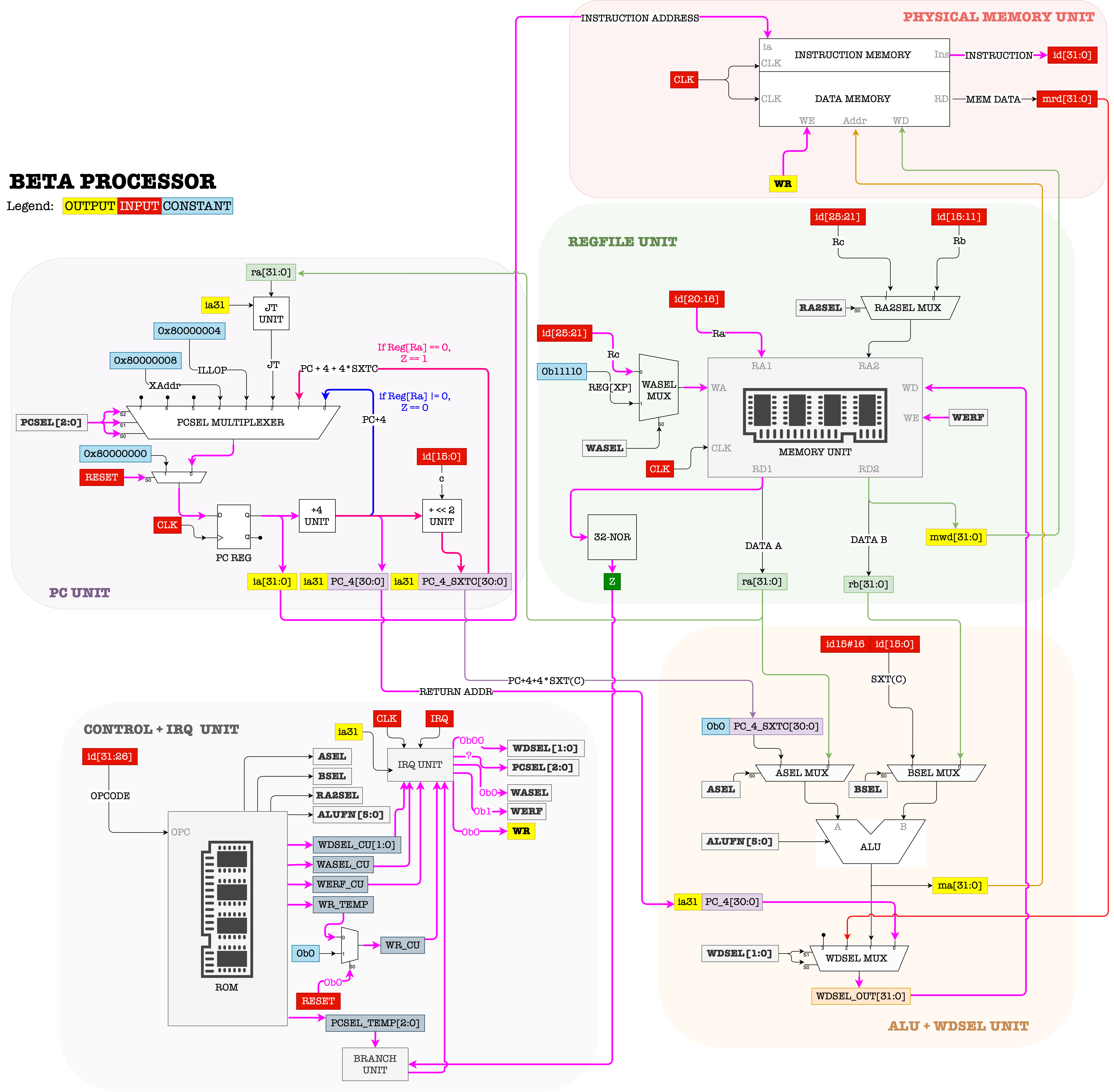
Control Signals
ALUFN = --- We aren’t using the ALU at all when transferring control, so we don’t care about what values goes as
ALUFN.
- We aren’t using the ALU at all when transferring control, so we don’t care about what values goes as
WERF = 1BSEL = --WDSEL = 00WR = 0RA2SEL = --PCSEL = Z ? 001 : 000ASEL = --WASEL = 0
BNE datapath
Purpose
BNE is similar to BEQ, but branches PC in the opposite way, i.e: when Ra != 0. It also utilizes the output Z.
The general format of the BNE instruction is:

Register Transfer Language
PC \(\leftarrow\) PC+4
Reg[Rc] \(\leftarrow\) PC
EA \(\leftarrow\) PC + 4*SEXT(C)
if (Reg[Ra] != 0) then PC \(\leftarrow\) EA
Assembly Language Format
The corresponding assembly instruction format runnable in BSIM is BNE(Ra, label, Rc) where c is auto computed as (address_of_label - address_of_current_ins)/4-1
Datapath
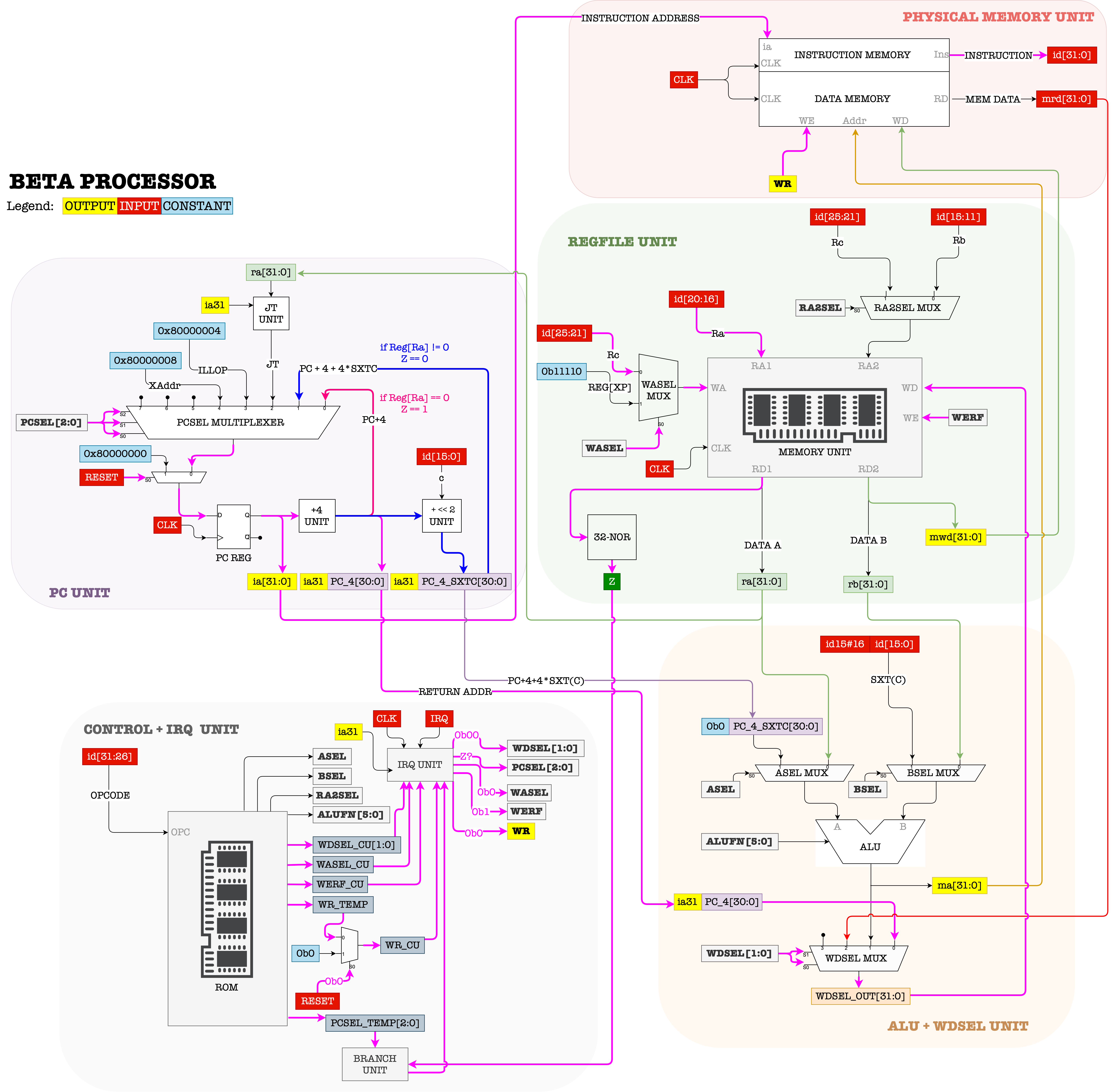
Control Signals
ALUFN = --WERF = 1BSEL = --WDSEL = 00WR = 0RA2SEL = --PCSEL = Z ? 000 : 001ASEL = --WASEL = 0
JMP Datapath
Purpose
JMP also allows the CPU to change its PC value, but without any condition (hence the name: jump). The address of the instruction following the JMP instruction is written to Rc, then PC is loaded with the contents of Ra. The low two bits of Reg[Ra] must be masked (force set to 00) to ensure that the target address is aligned on a 4-byte boundary.
Think!
If
Reg[Ra]is0x00001357, we can force it’s lower to bits to be00, by doing aBITWISE ANDwith mask0xFFFFFFFChence resulting in0x00001354. Why do we need to do this?
The general format of the JMP instruction is:

Register Transfer Language
PC \(\leftarrow\) PC+4
Reg[Rc] \(\leftarrow\) PC
EA \(\leftarrow\) Reg[Ra] & 0xFFFFFFFC (masked)
PC\(\leftarrow\) EA
- The corresponding assembly instruction format runnable in BSIM is
JMP(Ra, Rc).
Datapath
Control Signals
ALUFN = --WERF = 1BSEL = --WDSEL = 00WR = 0RA2SEL = --PCSEL = 010ASEL = --WASEL = 0
Sample Code
Try it Yourself!
Run this code step by step on BSIM and observe the datapath to familiarize yourself with how OP and OPC datapath works.
- At each timestep, be aware of the value of PC and all Registers.
- Know where is the address of each instruction when loaded to memory
- Note how to translate from
labeltoliteralwhen crafting the 32-bit machine language forBEQ/BNEinstructions.
.include beta.uasm

ADDC(R31, 3, R0)

begin_check: CMPEQ(R31, R0, R1)
BNE(R1, is_zero, R10)
SUBC(R0, 1, R0)
BEQ(R31, begin_check, R10)

is_zero: JMP(R31)
More about RESET
The \(\beta\) processor accept external RESET signal that can reset the value of the PC. The signal RESET must be 1 for several clock cycles in order to ensure that the values affected by RESET propagates throughout the entire circuit. During the period where RESET = 1, we need to make sure that WR is 0 so that we do not accidentally overwrite the content of the physical memory.
How Does CPU Interpret Signed vs Unsigned Numbers?
The CPU hardware sees numbers purely as binary bit patterns. It does not inherently know if they represent signed or unsigned values. It’s similar to the word “bank”, which can mean either a financial institution or the side of a river in english. The meaning depends entirely on context.
For example, the binary number 11111111 can represent the unsigned value 255 or the signed value -1, and it’s the software (instructions) that explicitly tells the CPU how to interpret this pattern.
The CPU never interprets binary patterns as signed or unsigned. It simply performs arithmetic operations using circuits that handle binary patterns in specific ways (e.g., addition via ALU).
Software Handling
Software explicitly instructs the CPU how to interpret numbers as signed or unsigned through specific assembly instructions or by using data types in high-level programming languages. For example, in RISC-V:
- The instruction
addi(signed addition) andaddiu(unsigned addition) both perform exactly the same binary operation (addition) inside the CPU hardware. The CPU just adds bits, oblivious to signed or unsigned interpretation. - The difference comes afterward: software chooses to interpret the result as signed or unsigned depending on what was intended. For instance:
- Binary pattern:
11111111 - Signed interpretation (software-decided):
-1 - Unsigned interpretation (software-decided):
255 - If software executes an unsigned comparison instruction (like
bltu, branch less than unsigned), the CPU circuit checks this bit pattern as unsigned (255), and branches accordingly. - If software executes a signed comparison instruction (like
blt, branch less than), the CPU circuit checks the same bit pattern as signed (-1 in two’s complement), and branches differently.
- Binary pattern:
We design and build CPU hardware circuits (like ALUs and comparison units) that perform arithmetic differently for signed or unsigned instructions as explicitly requested by software.
Analogy
Software choosing interpretation is similar to specifying units when measuring something.
The hardware (CPU) is like a ruler that measures a length as “100”. Software decides explicitly whether that “100” is centimeters or inches, changing its interpretation and usage entirely.
CPU Benchmarking
We always want a CPU that has a high performance (most instruction per second) at a low cost. Unfortunately there will always be a tradeoff between the two. Although it is common to judge a CPU’s performance from its clock rate (cycles per second, typically ranging between 2-4 GHz per core for modern computers), we also need to consider another metric called the \(CPI\), that is the average clock cycles used to execute a single instruction.
We can benchmark the quality of a CPU by computing its \(MIPS\) (million instruction per second),
\[MIPS = \frac{Clock Rate }{CPI}\]where \(CPI\) means clocks per instruction.
\(\beta\) assembly language takes exactly 1 clock per instruction. However, this is not always true in general. Complex architectures like the x86 might require several cycles to perform a single instruction. Besides, if we loosely meant the benchmarking instruction as high-level instruction, then surely it takes more than 1 clock cycle to compute because they can be assembled into many lines of instructions.
For instance:
# assume x is at memory address 48 (just an arbitrary choice)
x = 3 # single line of assignment

# translates to at least 2 cycles in Beta
ADDC(R31, 3, R2)
ST(R2, 0x0030, R31)
Typically, one will choose a particular program (written in a particular language, e.g: c or Python) for benchmarking purposes, and the same benchmark program is run on different CPUs with potentially different Clock Rate and \(CPI\).
The higher the \(MIPS\), the faster it takes to run the benchmark program. Therefore we can say that a CPU with the highest \(MIPS\) has the best performance.
Summary
You may want to watch the post lecture videos here:
This notes focuses on the architecture and operation of the \(\beta\) CPU, a RISC-like architecture designed as an educational tool to help understand the principles of CPU design and operation.
Here are the key points from this notes:
- CPU Components and Functions: The Beta CPU includes a Program Counter (PC), Register Files (REGFILE), Arithmetic Logic Unit (ALU), and a Control Unit (CU). The PC determines the sequence of operations, REGFILE stores temporary data, ALU performs arithmetic and logical operations, and the CU directs all these activities based on the decoded instructions.
- Memory Interaction: Instructions are fetched from memory and executed by the CPU. This process involves the PC fetching the instruction address, the memory returning the instruction data, and the CU decoding and executing these instructions. Both data and instruction resides in the same memory unit (shares address space).
- Control Logic and Signals: The control unit uses various signals derived from the OPCODE of each instruction to control the flow of data and operations within the CPU. This includes signals for selecting operation types and directing data paths within the CPU. It is implemented as a ROM with 6 input bits (OPCODE) and 17 output bits: asel, bsel, ra2sel, pcsel (3 bits), wdsel (2bits), reset, werf (regfile write enable), alufn (6 bits), wr (memory write enable)
- Datapaths: The CPU’s datapaths are configured based on the type of instruction being executed, which can involve direct arithmetic operations, memory access, or control transfer instructions. These paths dictate how data moves through the CPU and how results are stored or used.
- Instruction Set and Encoding: The Beta CPU uses a specific set of 32 instructions (Type 1 and Type 2), each encoded in a standard format that the CU can interpret. They are generally divided into 3 categories: arithmetic operation (with and without constant), transfer of control function (JMP, BNE, BEQ), and memory access (LD, LDR, ST)
The Beta CPU detailed insight into how a simplified yet functional CPU operates, mirroring larger, more complex systems used in real-world computing (especially RISC family).
Next Time
We technically can write instructions in machine language (0s and 1s), but it is not user friendly at all. The next lecture introduces us to assemblers and compilers, which are softwares created to help us utilise the \(\beta\) CPU better (program more easily) so that we can be more focused on designing our program, and less time writing the program.