 50.002 CS
- Overview
- Cache Design Issues
- Comparing FA and DM Cache
- Improving Associativity with NWSA Cache
- Replacement Policies
- The Cache Block Size
- Write Policies
- The Helper Bits
- Word Addressing Convention
- Cache Benchmarking
- The Caching Algorithm
- Summary
- Appendix
50.002 Computation Structures
Information Systems Technology and Design
Singapore University of Technology and Design
Cache Design Issues
You can find the lecture video here. You can also click on each header to bring you to the section of the video covering the subtopic.
Detailed Learning Objectives
- Explain Cache and Its Role:
- Describe the function of cache in reducing CPU access time to memory.
- Identify the types of cache (L1, L2, L3) and understand their general function without detailed architectural differences.
- List out Cache Design Parameters:
- Explain the significance of cache size, block size, associativity, and read/write/replacement policies in cache design.
- Analyze how each parameter affects cache performance and cost.
- Differentiate Cache Types: DM and FA:
- Compare and contrast Direct Mapped (DM) and Fully Associative (FA) caches.
- Discuss the pros and cons of each type concerning performance, cost, and risk of contention.
- Explain Associativity in Caches:
- Define what associativity is in the context of caches and its importance in reducing contention.
- Explain N-Way Set Associative Cache as a hybrid approach between DM and FA caches.
- Assess Various Cache Replacement Policies:
- Examine common replacement strategies like Least Recently Used (LRU), Least Recently Replaced (LRR), and Random replacement.
- Discuss the hardware overhead and application scenarios for each replacement policy.
- Assess Various Cache Write Policies:
- Describe different write policies including Write-Through, Write-Back, and Write-Behind.
- Evaluate the trade-offs and complexities associated with each write policy.
- Assess Cache Block Size Considerations
- Analyze the impact of block size on cache efficiency and performance.
- Explain the trade-offs between fetching large blocks (pros) and the risk of fetching unused words (cons).
- Explain Cache Helper Bits
- Explain and justify the function of helper bits like Valid, Dirty, and LRU bits in cache operations.
- Discuss the storage requirements and implications of each type of helper bit on cache design.
- Perform Cache Performance Metrics and Benchmarking
- Compute cache performance at steady state using HIT and MISS rates.
- Use benchmarks to determine the effectiveness of different cache configurations and replacement policies.
These learning objectives are designed to guide students through understanding cache memory, its design considerations, and operational strategies in a computer system architecture course.
Overview
Recall that cache is a small and fast (and expensive, made of SRAM) memory unit assembled near the CPU core, which function is to reduce the average time and energy required for the CPU to access some requested data Mem[A] located in the Main Memory (RAM). You know them commercially as the L1, L2, or L3 caches. We simplify them in this course by just referring to them as a single level cache.
The cache contains a copy of some recently or frequently used data Mem[A] and its address A. The hardware is assembled in such a way that the CPU will always look for that particular data in the cache first, and only look for the requested information in the Physical Memory if cache MISS occurs (and then the cache will be updated to contain this new information).
The CPU is able to both read from the cache and write to the cache (like normal LD and ST to the RAM).
Without the presence of cache device, the CPU has to frequently access the RAM. Frequent LD and ST to the Physical Memory becomes the main bottleneck for CPU performance. This is because the time taken for a write and read operation in DRAM is significantly longer than the optimum CPU CLK cycle.
In this chapter, we will learn various cache design issues such as its (hardware) parameters: cache size, cache block size, associativity, and read/write/replacement policies.
Cache Design Issues
There are 4 categories of cache design issues:
- Associativity: refers to the decision on how many different cache lines can one address be mapped (stored) to. Of course note that there can only be one copy of that address (tag) in the entire cache.
- In a DM cache, there is no choice on which cache line is used or looked up. A 1-to-1 mapping between each combination of the last \(k\) bit of the query address
Ato the cache line (entry) is required. Hence, the DM cache has no associativity. - In an FA cache, it has complete associativity as the name suggests. We have
Nchoices of cache lines in an FA cache of sizeN: anyTag-Contentcan reside on any cache line in FA cache.
- In a DM cache, there is no choice on which cache line is used or looked up. A 1-to-1 mapping between each combination of the last \(k\) bit of the query address
-
Replacement policy: refers to the decision on which entry of the cache should we replace in the event of cache
MISS. -
Block size: refers to the problem on deciding how many sets of 32-bits data do we want to write to the cache at a time.
- Write policy: refers to the decision on when do we write (updated entries) from cache to the main memory.
Cache management involves decisions on associativity, replacement policy, block size, and write policy, each contributing to how effectively the cache operates within a computer system, influencing performance, efficiency, and complexity.
This note provides a brief overview of the key design considerations in cache architecture, highlighting how associativity, replacement policy, block size, and write policy play crucial roles in optimizing cache performance and managing data efficiently within a computer system. These factors are essential for ensuring that the cache operates effectively, balancing speed, capacity, and complexity.
Comparing FA and DM Cache
In the previous lecture, we were introduced to the Fully Associative (FA) and Direct-Mapped (DM) caches. Comparing these two types of caches will illustrate their distinct approaches and the practical implications of their design choices on system performance and efficiency.
| Metric | FA Cache | DM Cache |
|---|---|---|
TAG field |
All address bits | Higher T address bits |
Content field |
All N bits of Data: Mem[A] |
All N bits Data: Mem[A] |
TAG Indexing |
None | Lower K address bits |
| Cache Size | Any | \(2^K\) |
| Memory Cell Technology | SRAM | SRAM |
| Performance | Very fast (gold standard) | Slower than FA cache on average |
| Contention Risk | None | Inversely proportional to cache size |
| Cost | Expensive | Cheaper than FA |
| Replacement policy | LRU, FIFO, Random | Not Applicable |
| Associativity | Fully associative, any Tag-Content can be placed on any cache line |
None. Each cache line can only contain matching lower k-bits TAG |
Based on the above, we can draw the conclusion that the superiority of Fully Associative (FA) and Direct-Mapped (DM) cache architectures depends on specific performance needs, hardware constraints, and the nature of the workload.
Cases where FA Cache is superior:
- High Miss Penalty Environments: FA caches are most beneficial in scenarios where the cost of a cache miss is very high, as their flexibility in placement can significantly reduce miss rates, especially conflict misses.
- Irregular Access Patterns: In applications with irregular or unpredictable memory access patterns, FA caches excel because any block can be placed in any line, minimizing the risk of cache thrashing.
- Critical Performance Needs: For high-performance computing where every cache hit counts, the higher potential hit rate of an FA cache can be a crucial advantage.
- Small Cache Sizes: In systems where the cache size is limited, having a fully associative cache can help maximize the efficiency of the available space.
Cases where DM Cache is superior:
- Cost and Simplicity Concerns: DM caches are simpler and cheaper to implement due to their straightforward hardware design. This makes them suitable for budget-constrained projects or less complex processors.
- Predictable Access Patterns: When the access patterns are predictable and can be optimized to avoid conflicts, DM caches perform very well. This scenario is typical in embedded systems where the workload can be tightly controlled.
- Low-Latency Requirements: The simplicity of a DM cache also means that the lookup times are generally lower, providing faster access times which are crucial in time-sensitive applications.
- Larger Cache Sizes: As the cache size increases, the likelihood of conflicts in a DM cache decreases, making it more viable in scenarios where large caches are feasible.
Each cache type has its strengths and trade-offs, and the choice between FA and DM often comes down to balancing these factors against the specific requirements and constraints of the application and hardware environment.
Improving Associativity with NWSA Cache
N-Way Set Associative Cache (NWSA)
An NWSA cache is a hybrid design between FA and DM cache architecture.
Motivation
Although DM cache is cheaper in comparison to the FA cache, it suffers from the contention problem. Contention mostly occurs within a certain block of addresses (called independent hot-spots), due to the locality of reference in each different address range.
Contention Example
Consider a DM cache with 8 cache lines. If instructions for Program A lies in memory address range
0x1000to0x1111, and instructions for Program B lies in memory address range0xB000to0xB111, concurrent execution of Program A and B will cause major contention.
Hence, some degree of associativity is needed. Full associativity will be expensive, so we try to just have some of it.
N-Way Set Associative Cache
One way to increase the associativity of a DM cache is to build an N-way set associative cache (NWSA cache).
- NWSA cache will be cheaper to produce than FA cache (of the same storage capacity), but slightly more expensive than its full DM cache counterpart of the same size.
- NWSA cache has less risk of contention (proportional to the value of
N).
The figure below illustrates the structure of an NWSA cache:

An NWSA cache is made up of N DM caches, connected in a parallel fashion. The cells in the same ‘row’ marked in red is called as belonging in the same set. The cells in the same ‘column’ of DM caches is said to belong in the same way. Each way is basically a DM cache that has \(2^k\) cache lines.
To Write
Given a write address A, we segment it into K-bits lower address (excluding the LSB 00) and T bits upper address. We need to first find the set which this K bits belong to. That particular combination of K-bits lower address, its higher T bits TAG and its Content can be stored in any of the N cache lines in the same set.
To Read
Given a query address A, we will need to wait for the device to decode its last K bits and find the right set. Then, the device will perform a parallel lookup operation for all N cache lines in the same set. The lookup operation to find the cache line with the right content is done using bitwise-comparison with the T bits of the query address.
Replacement Policies
Cache replacement policy is required in both FA cache and NWSA cache (but not DM cache). In the event of cache MISS, we need to replace TAG-Content field of the old cache line with this newly requested one.
Think!
Why don’t we need a replacement policy for DM Cache?
There are three common cache replacement strategies: LRR, LRU, and Random. They are primarily implemented in hardware. This is necessary because cache operations—especially the decision-making around which cache blocks to replace on a cache miss—need to be executed rapidly to maintain high performance Each policy carries varying degree of overhead.
Overhead
An overhead is an additional cost (time, energy, money) to maintain and implement that feature.
Least Recently Used (LRU)
LRU
Always replace the least recently used item in the cache.
Overhead
There are two sources of overhead for LRU replacement policy:
-
We need know which item is the least recently used after each read/write access. That is, we need to keep an ordered list of
Nitems in the cache (FA) or set at all times. This takes up \(\log(N)\) bits per cache line. If we haveNcache lines, we have the space complexity of \(N\log_2(N)\) bits to contain the necessary information for supporting LRU replacement policy. This results in a bigger and more costly cache hardware. -
We also need a complex hardware logic unit for implementing LRU algorithm (some kind of sorting algorithm) and to re-order the LRU bits after every cache access. Such hardware unit which specialises in keeping a sorted data structure at all times with minimal computation time is very expensive.
Example
Suppose we have an FA cache of size N=4, and we access the following addresses in this sequence: 0x0004,0x000C,0x0C08,0x0004,0xFF00,0xAACC at t=0,1,2,3,4,5 respectively. We also assume that the smallest LRU bit indicates the most recently accessed data
At t=2, the state of the FA cache with LRU as replacement policy will be:
| TAG | Content | LRU |
|---|---|---|
0x0004 |
Mem[0x0004] |
10 |
0x000C |
Mem[0x000C] |
01 |
0x0C08 |
Mem[0x0C08] |
00 |
At t=3, we access A=0x0004 again. This updates all LRU bits:
| TAG | Content | LRU |
|---|---|---|
0x0004 |
Mem[0x0004] |
00 |
0x000C |
Mem[0x000C] |
10 |
0x0C08 |
Mem[0x0C08] |
01 |
At t=5, the entry 0x000C-Mem[0x000C] is replaced because its the least recently used entry:
| TAG | Content | LRU |
|---|---|---|
0x0004 |
Mem[0x0004] |
10 |
0xAACC |
Mem[0xAACC] |
00 |
0x0C08 |
Mem[0x0C08] |
11 |
0xFF00 |
Mem[0xFF00] |
01 |
The LRU bits is updated at every cache access, regardless of whether it triggers a replacement or not.
Least Recently Replaced (LRR)
LRR
Always replace the oldest recently used item in the cache, regardless of its last access time.
The LRR is essentially implemented in hardware as a pointer containing the index of the “oldest” item in the cache.
Overhead
An LRR replacement policy has comparably less overhead than LRU:
- We only need to know which is oldest cache line in the device.
- If there are
Nitems in the cache, we need to have a pointer of size \(O(\log_2 N)\) bits that can remember to the oldest cache line plus a simple (not as complex) logic unit to perform the LRR algorithm, that is to find the next oldest cache line.
Example
Suppose we have an FA cache of size N=4, and we request these addresses in sequence: 0x0004,0x000C,0x0C08,0x0004,0xFF00,0xAACC at t=0,1,2,3,4,5 respectively. Assume that we will always fill empty cache from the smallest index to the largest index.
Att=2, the state of the FA cache with LRR as replacement policy will be:
LRR: 00
| TAG | Content |
|---|---|
0x0004 |
Mem[0x0004] |
0x000C |
Mem[0x000C] |
0x0C08 |
Mem[0x0C08] |
At t=3, we access A=4 again, but the LRR pointer will not be updated.
At t=5, the one that is replaced is A=0x0004, and the LRR pointer can be increased to be the next oldest entry (the next index):
LRR: 01
| TAG | Content |
|---|---|
0xAACC |
Mem[0xAACC] |
0x000C |
Mem[0x000C] |
0x0C08 |
Mem[0x0C08] |
0xFF00 |
Mem[0xFF00] |
Random
Random Replacement
Always replace a random cache line.
Overhead
This policy has the least overhead when compared to LRR and LRU. We simply need some logic unit to behave like a random number generator, and we use this to select the cache line to replace when the cache is full.
Comparing Between Strategies
There’s no one superior replacement policy. One replacement policy can be better than the other depending on our use case i.e: pattern of addresses enquired/accessed by CPU.
Refer to our Problem Set for various exercises with all 3 replacement policies.
Random replacement policy is the simplest to implement as it does not require much additional hardware overhead. However in practice, LRU may generally gives a better experience because it conforms to locality of reference, and is better when N is small (since it is expensive to implement). LRR is performs well on specific pattern of usage where we don’t frequently revisit oldest cached data. Finally, random method is preferable when N is super large, which in turn will be too costly to implement LRU or LRR.
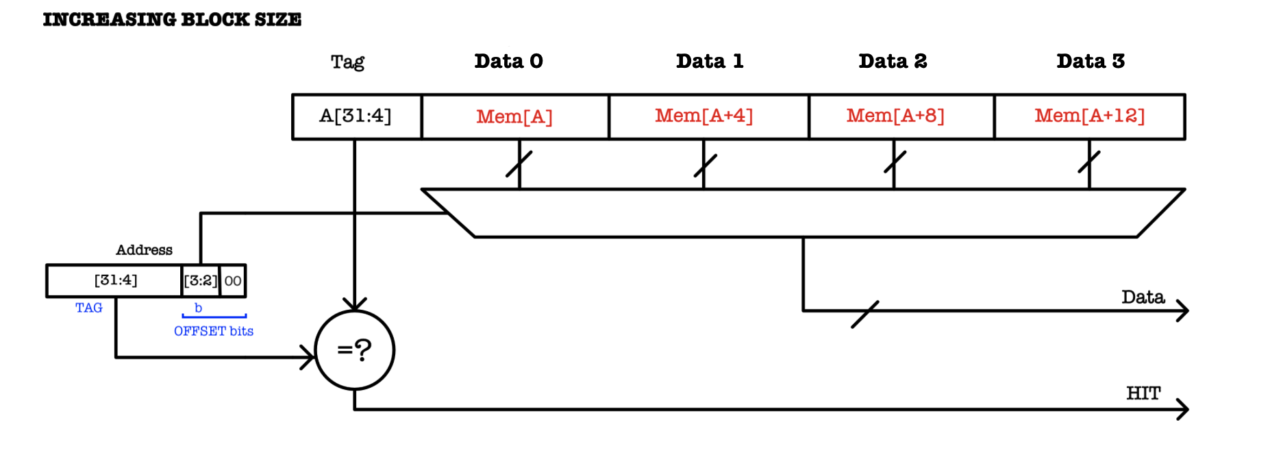
The Cache Block Size
Expanding the content in each cache line
We can further improve cache performance by expanding the content stored in each cache line. We do this by fetching
Bdata words at a time to and from the RAM (Physical Memory).
This method is especially useful if there’s high locality of reference. The figure below illustrates a cache with a single cache line with block size of 4:
If we have a DM cache with $N$ cache lines and block size of 4: how many TAG, k, and b bits are there?
The number of data words stored in each cache line is called the block size and is always a power of two. Recall that 1 word = 32 bits for the \(\beta\) CPU, and we address the entire word by its smallest byte address, e.g: word address 0 is comprised of data at address 0 to 3.
Hence to index or address each word in the cache block of B words, we need \(b = \log_2(B)\) bits. In the example above, we need 2 bits to address each column, taken from A[3:2] (assuming that A uses byte addressing).
The Offset bits
Some literature calls the
b+2bits as the offset bits. Offset bits in a cache refer to the part of the memory address used to determine the exact location within a cache line where the desired data is stored. Offset corresponds to the bits used to determine the byte to be accessed from the cache “row”. In the example above, because the cache “row” is 4 words long (16 bytes long), there are 4 offset bits: the 2bbits + 2.
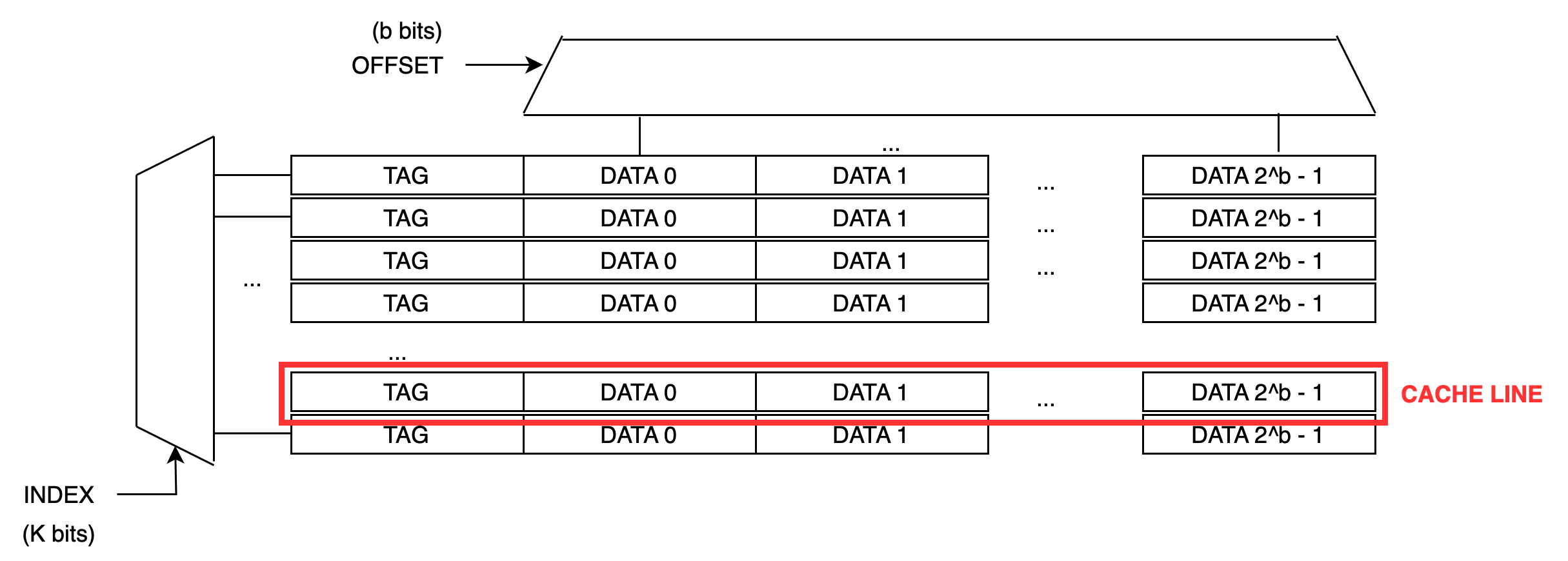
What is a Cache Line when Block Size > 1?
There might be no single universal definition of what a cache line is when block size > 1. It can mean a single row, or a single word of content.
You might even see words like cache block instead of cache line when block size > 1. These two terms are often used interchangeably in modern texts (Patterson & Hennessy, Bryant & O’Hallaron, and industry), where both refer to one row in a DM cache.
However, older hardware-oriented texts distinguish them as follows: a cache line is a single word, and a cache block is a full row containing N cache lines.
In this course, we shall follow the modern convention wherever possible. We will make it very clear in exams as well by stating the total cache’s capacity (in words) too.
In summary, if we have block size of 8 for example with word addressing:
- In a DM cache, a cache line refers to a row with 8 data words (content), all sharing the same
TAG(figure below) - In a NWSA cache, a cache line means the same thing, but for a single way (a single DM cache with that 8 data words of content). Multiple cache lines sharing the same index is called a set.
Tradeoffs
There are tradeoffs in determining the block size of our cache, since we always fetch (and / or overwrite) B words – the entire block – together at a time. For instance, with a block size of 4, a missed access to address 0 will cause data word at address 0, 4, 8, and 12 to be fetched altogether from memory. Another example: a missed access to address 20 will cause data word at address 16, 20, 24, and 28 to be fetched altogether as well.
- Pros: If high locality of reference is present, there’s high likelihood that the words from the same block will be required together. Fetching a large block upon the first
MISSwill be beneficial later on, thus improving the average performance. - Cons: Risk of fetching unused words. With a larger block size, we have to fetch more words on a cache
MISSand theMISSpenalty grows linearly with increasing block size if there’s low locality of reference.
Write Policies
When the CPU executes a ST instruction, it will first write the cache line: TAG = Address, Content = new content. We will then have to decide when to actually update the physical memory. Sometimes we do not need to update the physical memory at each ST as what was stored might only be intermediary or temporary values. This is where the act of “writing to cache first” instead of directly to physical memory speeds up execution.
To update the physical memory, the CPU must first fetch the data from the cache to the CPU register, and then write it (with ST instruction) to the physical memory. This pauses execution of the ongoing program as the CPU will be busy writing to the physical memory and updating it.
There are three common cache write strategies: write-through, write-back, write-behind.
Write-through
Write Through
CPU writes are done in the cache first by setting
TAG = Address, andContent = new contentin an available cache line, and is also immediately written to the physical memory.
This policy stalls the CPU until write to memory is complete, but memory always holds the “truth”, and is never oudated.
Write-back
Write Through
CPU writes are done in the cache first by setting
TAG = Address, andContent = new contentin an available cache line, but not immediately written to the main memory.
As a consequence, the contents in the physical memory can be “stale” (outdated).
To support this policy, the cache needs to have a helper bit called the dirty bit (see next section for more information) for each cache line. This bit indicates whether the corresponding copy of the content in the main memory is outdated. The CPU will write to the physical memory only if the data in cache line needs to be replaced and that the cache line is dirty. If the data is not dirty, then the cache line can simply be replaced without any writes.
Write-behind
Write Behind
CPU writes are also done in the cache first by setting
TAG = Address, andContent = new contentin an available cache line. Afterwards, the update of the physical memory is immediate but buffered or pipelined using other supporting hardware.
This policy might require slightly complex hardware to implement as opposed to the other policies, e.g: hardware to support this pipelined update of the physical memory. CPU will not stall and will be executing next instructions while writes are completed in the background. It also needs the dirty bit indicator that will be cleared once the background write finishes.
It is not trivial to do this because now we require an additional hardware unit that is asynchronous to the CPU clock. It does not depend on the CPU to run and therefore we need to consider some kind of fail-safe feature to synchronise between the CPU and this pipeline system when needed.
There is no best write policy. Think about the pros and cons of each policy, and think about specific cases where one policy is superior than the other.
The Helper Bits
The cache device may need to store not just Tag and Content per cache line, but also some helper bits that are used to perform some write or replacement policy, and the overall caching algorithm.
V: Valid Bit
The valid bit (either 1 or 0) is used to indicate whether the particular cache line contains valid (means important) values, for example valid copy of data from memory unit and not an invalid or garbage values.
Why do we need the valid bit?
In electronics, information is encoded in voltage. The device do not know what is the difference in usage between valid information vs invalid gibberish in a memory cell until it attempts to compute its value – which takes time. It does not know the difference between redundant (old) information vs new information. Therefore the valid bit is used as a quick indicator whether the content in the cache line is important or not.
The cache performance can be further sped up if it is made to check (compare TAG) if V = 1 for the cache line – and skip comparison of TAG when V=0 which takes longer time than a simple 1-bit comparison of V==1. This allows for a faster HIT computation in the event of cache MISS.
Cost
The V bit requires just 1 extra storage bit per cache line. For cache lines with block size larger than 1, there’s still only one V bit per cache line (so the entire b block of words are either present or not present).
D: Dirty Bit
The dirty bit (1 or 0) is used to indicate whether we need to update the memory unit to reflect the new updated version in the cache. The dirty bit is set to 1 if and only if the cache line is updated (CPU writes new values to cache) but this new value hasn’t been stored to the physical memory. In other words, the copy in the physical memory is outdated.
LRU: Least Recently Used Bits
The LRU bit is present in each cache line for FA and NWSA cache only regardless of the block size (not DM cache because DM cache does not have a replacement policy). For a cache with associativity N, we need N log N bits in total to store the LRU bit alone.
The helper bits can be illustrated in a diagram like below. Below we have a sample of 3WSA cache with block size of 2:

How many LRU bits?
The diagram above illustrates a 3-Way SA cache with 3 distinct sets. How many LRU bits are needed per cache line? How many LRU bits are needed for the whole cache hardware, i.e: how many SRAM cells are needed to hold ALL LRU bits in the entire cache hardware?
Word Addressing Convention
Previously, we learned that byte addressing is used by convention. However for ease of calculation in practice questions and problem sets, we can use WORD addressing instead (we give an address for each word instead of each byte).
Given a memory unit of fixed size M, can use 2 bits less if we were to use word addressing instead of byte addressing.
For DM/NWSA cache with B blocks and word addressing, we need to divide the original requested address into the same three segments, but we don’t have the default 00 in the lowest 2 bits of the address (as when byte addressing is used) anymore:
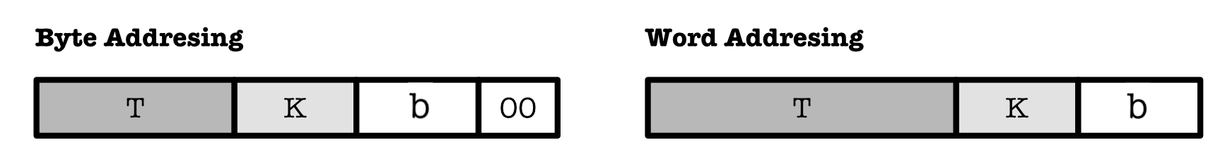
Details:
- Lowest
b-bits to index each word in a cache line block. K-bits to index each cache line or set.- Highest (remainder)
T-bits of the original requested address to be stored in theTAGfield.
Cache Benchmarking
We can compute average cache performance by counting how many HITs (and MISS) are there given N queries in sequence, and dividing the number of HIT with N, given its hardware specification such as block size, replacement policy, and cache size.
If the query sequences repeat itself, that means we have reached the steady state. we can compute the number of HIT and MISS from its steady state.
Read the given question carefully. Not all questions will ask you about steady state performance, sometimes we might simply ask you to compute whether a given address sequence results in a series of HIT or MISS. However if we want to systematically measure cache performance, we typically measure its steady state performance.
Example
We want to measure the performance of an FA cache that has 4 cache lines with LRR replacement policy.
Assume that the cache is initially empty (or contains redundant values – nothing relevant is cached before), we let the CPU execute the following program consisted of 9 READ (LD) requests for a few rounds:
At t=0: 0x0014
At t=1: 0x0011
At t=2: 0x0022
At t=3: 0x0014
At t=4: 0x0043
At t=5: 0x0012
At t=6: 0x0014
At t=7: 0x00AB
At t=8: 0x0033
We repeat the same 9 input sequences again for the second “round”:
At t=9: 0x0014
At t=10: 0x0011
At t=11: 0x0022
At t=12: 0x0014
At t=13: 0x0043
At t=14: 0x0012
At t=15: 0x0014
At t=16: 0x00AB
At t=17: 0x0033
And repeated again, for the third “round”, and so on.
For the ease of computation, word addressing is used (you can also tell that this is true as the addresses no longer have the suffix 00). To benchmark this cache, we need to count how many MISS and HIT are there at the steady state. Hence, we need to figure out which rounds make up the steady state.
At the first round, t=0 to t=8, we have:
At t=0: 0x0014 \(\rightarrow\) MISS (and cached)
Cache content after this access: 0x0014, EMPTY, EMPTY, EMPTY. Oldest entry is removed and new entry is shown on the right.
At t=1: 0x0011 \(\rightarrow\) MISS (and cached).
Cache content after this access: 0x0014, 0x0011, EMPTY, EMPTY.
At t=2: 0x0022 \(\rightarrow\) MISS (and cached).
Cache content after this access: 0x0014, 0x0011, 0x0022, EMPTY.
At t=3: 0x0014\(\rightarrow\) HIT
At t=4: 0x0043\(\rightarrow\) MISS (and cached)
Cache content after this access: 0x0014, 0x0011, 0x0022, 0x0043.
At t=5: 0x0012 \(\rightarrow\) MISS (and cached by replacing oldest entry:0x0014)
Cache content after this access: 0x0011, 0x0022, 0x0043, 0x0012.
At t=6: 0x0014\(\rightarrow\) MISS (and cached by replacing oldest entry:0x0011)
Cache content after this access: 0x0022, 0x0043, 0x0012, 0x0014.
At t=7: 0x00AB \(\rightarrow\) MISS (and cached by replacing oldest entry:0x0022)
Cache content after this access: 0x0043, 0x0012, 0x0014, 0x00AB.
At t=8: 0x0033 \(\rightarrow\) MISS (and cached by replacing oldest entry:0x0043)
Cache content after this access: 0x0012, 0x0014, 0x00AB, 0x0033.
Now during the second round, t=9 to t=17, we have the same 9 input sequences. Let’s observe the result:
At t=9: 0x0014 \(\rightarrow\) HIT
At t=10: 0x0011 \(\rightarrow\) MISS (and cached by replacing oldest entry:0x0012)
Cache content after this access: 0x0014, 0x00AB, 0x0033, 0x0011.
At t=11: 0x0022 \(\rightarrow\) MISS (and cached by replacing oldest entry:0x0014)
Cache content after this access: 0x00AB, 0x0033, 0x0011, 0x0022.
At t=12: 0x0014\(\rightarrow\) MISS (and cached by replacing oldest entry:0x00AB)
Cache content after this access: 0x0033, 0x0011, 0x0022, 0x0014.
At t=13: 0x0043\(\rightarrow\) MISS (and cached by replacing oldest entry:0x0033)
Cache content after this access: 0x0011, 0x0022, 0x0014, 0x0043.
At t=14: 0x0012 \(\rightarrow\) MISS (and cached by replacing oldest entry:0x0011)
Cache content after this access: 0x0022, 0x0014, 0x0043, 0x0012.
At t=15: 0x0014\(\rightarrow\) HIT
At t=16: 0x00AB \(\rightarrow\) MISS (and cached by replacing oldest entry:0x0022)
Cache content after this access: 0x0014, 0x0043, 0x0012, 0x00AB.
At t=17: 0x0033 \(\rightarrow\) MISS (and cached by replacing oldest entry:0x0014)
Cache content after this access: 0x0043, 0x0012, 0x00AB, 0x0033.
Running the cache for another round (the third time) at t=18 to t=26 with the same 9 input sequences:
At t=18: 0x0014 \(\rightarrow\) MISS (and cached by replacing oldest entry:0x0043)
Cache content after this access: 0x0012, 0x00AB, 0x0033, 0x0014.
At t=19: 0x0011 \(\rightarrow\) MISS (and cached by replacing oldest entry:0x0012)
Cache content after this access: 0x00AB, 0x0033, 0x0014, 0x0011.
At t=20: 0x0022 \(\rightarrow\) MISS (and cached by replacing oldest entry:0x00AB)
Cache content after this access: 0x0033, 0x0014, 0x0011, 0x0022.
At t=21: 0x0014\(\rightarrow\) HIT
At t=22: 0x0043\(\rightarrow\) MISS (and cached by replacing oldest entry:0x0033)
Cache content after this access: 0x0014, 0x0011, 0x0022, 0x0043.
At t=23: 0x0012 \(\rightarrow\) MISS (and cached by replacing oldest entry:0x0014)
Cache content after this access: 0x0011, 0x0022, 0x0043, 0x0012.
At t=24: 0x0014\(\rightarrow\) MISS (and cached by replacing oldest entry:0x0011)
Cache content after this access: 0x0022, 0x0043, 0x0012, 0x0014.
At t=25: 0x00AB \(\rightarrow\) MISS (and cached by replacing oldest entry:0x0022)
Cache content after this access: 0x0043, 0x0012, 0x0014, 0x00AB.
At t=26: 0x0033 \(\rightarrow\) MISS (and cached by replacing oldest entry:0x0043)
Cache content after this access: 0x0012, 0x0014, 0x00AB, 0x0033.
If we run it again for the fourth round, we will have the same HIT and MISS sequences as the second round. This implies that the result of running it for the fifth round will be identical to the third round.
Hence on average we can count the number of HIT for the second and third round: 3 HIT in total for 18 address calls. We ignore results from the first round because that result will never repeat itself again as we begin with empty cache only once in the beginning.
That means out of the 18 address calls, we have 15 MISS. The miss rate of this cache is therefore pretty high at \(83.33\%\).
Practice
If the FA cache above uses LRU policy instead of LRR, will it have a better performance (more HIT, less MISS)?. What about when DM cache of same size (4 cache lines) is used? Which cache design is better for this particular program running in a loop?
The Caching Algorithm
The caching algorithm dictates the required actions of the cache in response to key events:
- Read/Write Requests: When the CPU sends a read or write request, the cache must determine whether the requested data is already in the cache (a cache hit) or if it needs to be retrieved from the main memory (a cache miss). In the case of a write request, the cache must also handle the data according to its write policy.
- Cache Replacement: If the cache is full and needs to accommodate new data, the caching algorithm applies the selected replacement policy to decide which existing items to evict in order to make room.
- Writing Back to Memory: The cache must decide when and how to write updated values back to the physical memory, which is dictated by the chosen write policy, such as write-through or write-back.”
The actual implementation of the caching algorithm is done via hardware implementation to achieve the fastest possible performance.
READ/LOAD request
On CPU READ/LOAD request for address A:
	check for A in TAG field of cache lines with V==1

	if HIT:
		update all helper bits necessary (e.g: if LRU used)
		return the corresponding content from cache to CPU

	else if MISS:
		if DM cache:
			selected cache line to replace
			is cache line with index matching last K bits of A
		else if FA cache:
			selected cache line to replace
			depends on replacement policy
		else if NWSA cache:
			selected cache line to replace
			depends on replacement policy in the set with index matching last K bits of A

		if cache line is dirty:
			if write policy == WRITE-BACK:
				compute the content's address
				and update physical memory
			else if write policy == WRITE-BEHIND:
				wait until update is done

		// at this point, selected cache line is safe to be overwritten

		fetch A and Mem[A] from physical memory

		if DM cache:
			write higher T bits of A to the
			TAG field of the selected cache line,
			and Mem[A] as its content

		if FA cache:
			write A to TAG field of the
			selected cache line, and Mem[A]
			as its content

			if replacement policy == LRU:
				update LRU bit
			else if replacement policy == LRR:
				update LRR pointer

		return Mem[A] to CPU
WRITE/STORE request
Why do we need to fetch data from memory first (if miss) during write?
In cache-based systems, the unit of transfer between memory and cache is the entire block (e.g., 64 bytes), not just the single word or byte you’re writing. Even if you’re only writing one word, the cache must first fetch the entire block from memory to preserve the rest of the data in that block. This ensures future reads to nearby addresses within the same block return correct data. Without fetching first, you’d risk overwriting part of the block while leaving the rest undefined or stale.
On CPU WRITE/STORE (new_content) request to address A:

	check for A in TAG field of cache lines with V==1

	if MISS:
		fetch word from memory
		if DM cache:
			selected cache line to replace
			is cache line with index matching last K bits of A
		else if FA cache:
			selected cache line to replace
			depends on replacement policy
		else if NWSA cache:
			selected cache line to replace
			depends on replacement policy in
			the set with index matching last K bits of A

		if cache line is dirty:
			if write policy == WRITE-BEHIND:
				wait
			else if write policy == WRITE-BACK:
				compute the content's address
				and update physical memory

	// at this point the cache line is safe to be overwritten or HIT
	if DM cache:
		write higher T bits of A to the
		TAG field of the selected cache line,
		and  new_content from CPU as its content

	if FA cache:
		write A to TAG field of the
		selected cache line,
		and new_content from CPU as its content

		if replacement policy == LRU:
			update LRU bit
		else if replacement policy == LRR:
			update LRR pointer

	if write policy == WRITE-THROUGH:
		compute the content's address
		and update physical memory
		return to CPU
	else:
		set cache line's dirty bit to 1
		return to CPU
Summary
You may want to watch the post lecture videos here.
Here are the key points from this notes:
- The four cache design issues: The four cache design issues discussed in this chapter are: associativity, replacement policies, write policies, and block size. We then explore the trade-offs between different cache associativities like DM cache and FA cache. There is no golden cache design that suits all kinds of situations. The performance of a cache depends on its use case and we need to choose our cache design wisely based on our use cases. For example, associativity is less important when
N(size of cache) is large, because the risk for contention is inversely proportional toN. - Cache Coherence and Management: Ensures that an alteration of the values in one cache is immediately reflected in all other memory region where that data is stored (the TLB and the Memory).
- Various replacement policies and their hardware implications:
- Associativity: NWSA caches map each block to a specific set, where we can have N cache lines in a specific set (adding some degree of associativity)
- Replacement Policies: Caches can be made to decide which block to replace when new data comes in. Policies covered are: LRU, LRR, and Random.
- Block Size: Considers the pros and cons of increasing cache block size, noting that while it may reduce the number of cache misses, it also risks increasing the fetch time for larger blocks.
- Write Policies: Write-Through, which immediately writes data to both cache and memory, Write-Back, which waits until the data is evicted from cache, and Write-Behind, which pipelines a cache write in the background (require additional hardware support)
- Helper Bits: Valid, Dirty, and LRU bits required to maintain data integrity and cache coherence.
- Cache Benchmarking: In practice, we can analyse cache performance by running diagnostics code and computing average access time.
Appendix
Hardware Implementation of Caching Algorithm
The implementation of caching algorithms via hardware is essential for achieving the fastest possible performance. This is crucial because the efficiency of cache operations directly impacts the overall speed and responsiveness of the computing system. Here are some additional details that underscore the importance of hardware implementation:
-
Speed: Hardware implementation allows caching decisions to be made at the speed of the processor’s clock cycles, which is necessary for maintaining the performance levels expected in modern computing environments.
-
Complexity Handling: Hardware mechanisms are designed to handle complex algorithms for managing cache, such as those for determining which data to cache (caching policy), which data to replace (replacement policy), and when to write data back to the main memory (write policy). These mechanisms are optimized to execute these tasks with minimal latency.
-
Direct Integration: By integrating the caching logic directly into the CPU or within close proximity to it, data travel time is minimized, further reducing latency and increasing the speed of data retrieval and storage operations.
-
Autonomy: Hardware-based cache management operates independently of the system’s main processor, allowing it to manage data in the background efficiently without burdening the CPU. This helps in multitasking environments where the processor needs to handle multiple tasks simultaneously.
Implementing caching strategies in hardware ensures that these critical functions do not become bottlenecks, thus supporting high-performance computing needs effectively.