 50.002 CS
- Overview
- Overview of Technology
- Memory Addressing
- The Memory Hierarchy Idea
- The Cache Idea
- Types of Cache Design
- Summary
- Appendix
50.002 Computation Structures
Information Systems Technology and Design
Singapore University of Technology and Design
Memory Hierarchy
You can find the lecture video here. You can also click on each header to bring you to the section of the video covering the subtopic.
Detailed Learning Objectives
- Describe the Overview of Memory in Computing Systems
- Explain the role of the REGFILE and external Memory Units in the \(\beta\) CPU architecture.
- Discuss the limitations of a 32-bit address space, which can address up to 4GB of memory.
- Explain the design of two Memory Technologies: SRAM and DRAM
- Explain Static Random-Access Memory (SRAM) and Dynamic Random-Access Memory (DRAM) as two primary technologies for creating memory cells.
- Describe the construction and operation of SRAM and DRAM, including the processes of reading from and writing to these memory types.
- Explain the volatility of these memory types and the need for power to retain data.
- Explain SRAM vs DRAM Characteristics
- Outline the differences in cost, speed, and capacity between SRAM and DRAM.
- Question how data is accessed and managed in both SRAM and DRAM cells.
- Discuss Application of Memory Technologies
- Discuss the practical use of SRAM and DRAM in modern computing, particularly in the context of consumer-grade PCs and CPU caches.
- Explain the role of the cache in enhancing processing speed by storing frequently accessed data closer to the CPU.
- Justify The Memory Hierarchy Concept
- Defend the idea of a memory hierarchy to achieve an optimal balance between speed, cost, and capacity.
- Describe the roles of various storage types within this hierarchy, including registers, cache, main memory (RAM), and disk storage.
- Explain Locality of Reference
- Discusse the principle of locality of reference, which predicts that certain memory locations are more likely to be accessed repeatedly over short periods.
- Explain how this principle supports the effective use of cache memory.
- Explain Cache Operation and Management
- List out various operations that can be done on a cache, including the concepts of cache hits and misses.
- Describe the processes involved when the cache does not contain requested data, including fetching data from main memory or disk.
- Draw and Explain Basic Cache Design Types: Fully Associative and Direct Mapped
- Explain the design of fully associative and direct mapped cache designs.
- Discusse the advantages and challenges associated with each design, including speed, cost, flexibility, and contention issues.
These notes are designed to give students a thorough understanding of the critical components and concepts related to memory technologies in computing systems, emphasizing the practical applications and the importance of memory hierarchy in achieving efficient computing operations.
Overview

So far we have learned that the \(\beta\) CPU has its own storage unit called the REGFILE, consisted of a limited amount of registers. The \(\beta\) can also write to or read from an external Memory Unit. This Memory Unit can be of any size, depending on how many bits are the used for addressing.
A 32-bit address can address \(2^{32}\) different bytes, and therefore can be used to address up to 4GB of data.
Since \(\beta\) is a 32-bit CPU, it can supply at most 32-bit of address to the Memory Unit, and therefore can have an access to at most 4GB of address space at a time without the help of other hardware.
This limitation can be removed on certain x86 32-bit architectures via the use of a particular memory management hardware called the PAE (Physical Address Extension). PAE was first introduced by Intel in their Pentium Pro processor, and later by AMD (Athlon processor). We will not touch about PAE in this course.
The REGFILE in \(\beta\) is very expensive to manufacture, but they are extremely fast, meaning that we can write to or read from the REGFILE unit at a very high frequency (low latency). Since REGFILE is a very expensive memory device, we can only afford to pack a few registers within the CPU while keeping it at a reasonable cost, and extend the storage space using some external memory device we previously label as The Memory Unit.
The materials that make up the external memory unit should be cheaper (than those that make up the REGFILE), hence we can have bigger storage space at a fraction of the price (and we won’t have to spend so much money just to buy a reasonably practical computer).
The Caveat
Depending on the technology, writing to or reading from the external memory unit can be much slower (than writing to and reading from the REGFILE), and therefore memory access becomes the bottleneck of the computer performance.
SRAM vs DRAM Overview
In this chapter, we will learn a couple more technologies that are commonly used to create 1-bit memory cell. They’re called SRAM and DRAM, with varying cost and latency. They’re summarised below:
\[\begin{matrix} \text{Types} &\text{Space} & \text{Latency} & \text{Cost} & \text{Volatile}\\ \hline \text{Register} & 100\text{'s of bytes} & 20ps & \$\$\$\$ &\text{Yes}\\ \text{SRAM} & 100\text{'s of Kbytes} & 1ns & \$\$\$ &\text{Yes}\\ \text{DRAM} & 100\text{'s of Mbytes} & 40ns & \$&\text{Yes}\\ \text{NAND Flash (SSD)} & 100\text{'s of Gbytes} & 400 us & cc&\text{No}\\ \text{Disk} & 100\text{'s of Gbytes} & 10 ms & c&\text{No}\\ \hline \end{matrix}\]Goal
Bear in mind that our ultimate goal is to have large memory space at a cheap cost and minimum latency. We can do that by incorporating the concept of memory hierarchy in our computer system.
Overview of Technology
Static Random-Access Memory (SRAM)
An SRAM cell can be made up of 6-transistors as shown in the figure below. It is also commonly called as the 6T-SRAM cell

Each cell stores one bit. The loop formed by two inverters can store a single bit for as long as they are powered. SRAM is a volatile memory device since it can only retain information when powered.
There are two other features to note:
- The word line: set to high voltage to “access” the cell
- The two complementary bit lines. These two complementary bit lines are connected to a sense amplifier.
The cell has both a bit line and a complement bit line because it is faster to tell the difference between voltage values than to wait until a valid voltage value reaches acceptable level in a single bit line. A sense amplifier’s role is to sense the low power signal difference from both bitlines and amplify the small voltage swing to recognizable logic level so the data can be interpreted quickly by logic units outside the memory.
The cell above shows a cell with bit 1 stored as its content. That is because when you activate the WORD line, the value 1 will be present at the bit line. This signifies the value of the cell.
For illustration purposes, the placement of the value 1 at the side of bit line matters. If that value were to be 0, then this cell is said to store bit value 0.
To Read
To read from an SRAM cell:
- Supply high voltage to the word line. This will connect the source and the drain of both NFETs.
- In turn, current flows to the bit line on the right and its complement on the left.
- The sense amp at the end of both bit-lines will compute the difference and amplify the small voltage difference to a valid 1-bit logic level.
For example, if the sense amp computes a +vedifference between \(V_{\text{bit}} - V_{\overline{\text{bit}}}\), then it corresponds to logic 1 and vice versa. As mentioned, the value of the cell in the figure above is 1.
To Write
To write to an SRAM cell:
- Supply high voltage to the word line.
- Then, drive a strong high voltage or strong low voltage through the bit line and its complement as shown to overwrite the existing cell’s value.
In this example, the value of the cell is written to be 0.

Dynamic Random-Access Memory (DRAM)
A single DRAM cell is capable of storing 1-bit of data by using just single NFET and a single capacitor when powered. It is also commonly called as 1T-DRAM cell. DRAM is also a volatile memory device.

To Read
To read from a DRAM cell, we do:
- Supply high voltage to the word line, and this will switch the NFET
on. - Read the output voltage on the bit line.
- Charges can flow to the bit line when there’s direct connection between the capacitor and the bit-line.
- There’s no sense amp in a DRAM cell, hence reading is slow (compared to reading an SRAM cell) because we need to wait for some time for the charge to accumulate at the bit line and give a valid digital voltage value.
We don’t really need to dive into details of how capacitor work. The ability of the capacitor to store a charge is called capacitance, and it is affected by the dielectric materials of the plates and the plates’ dimension.
To Write
To write to a DRAM cell, we do:
- Supply high voltage to the word line, and this will switch the NFET
on. - Supply strong
1or0through the bit line to charge or discharge the capacitor.
DRAM Issue
The major problem with DRAM is that the capacitor will leak charge over time, so the voltage value stored in the cells will fade (get corrupted) over time. To tackle this problem, each DRAM cell has to be refreshed very frequently to keep the data intact. These refresh cycles cause DRAM to be significantly slower than SRAM, although a DRAM cell is cheaper to make as compared to an SRAM cell (fewer number of transistors in a DRAM cell).
For instance, the RAM Corsair Vengeance LPX DDR4-3200 (CL16), sold in 8GB or 16GB modules advertises 25.6 GB/s bandwidth. However, periodic refresh cycles (tRFC, tREFI) temporarily block memory access. This leads to around 4–5% performance loss, reducing real-world bandwidth to about 24.5 GB/s. This refresh overhead isn’t shown in consumer specs but affects actual performance.
| Spec | Value |
|---|---|
| Advertised Speed | DDR4-3200 |
| Data Rate | 3200 MT/s |
| Bus Width | 64 bits = 8 bytes |
| Theoretical Bandwidth | 3200 × 8 = 25.6 GB/s |
| tRFC (Refresh Cycle Time) | ~350 ns |
| tREFI (Refresh Interval) | ~7.8 µs |
| % Time Lost to Refresh | ~4.5% |
| Estimated Real Bandwidth | ~24.5 GB/s |
Application
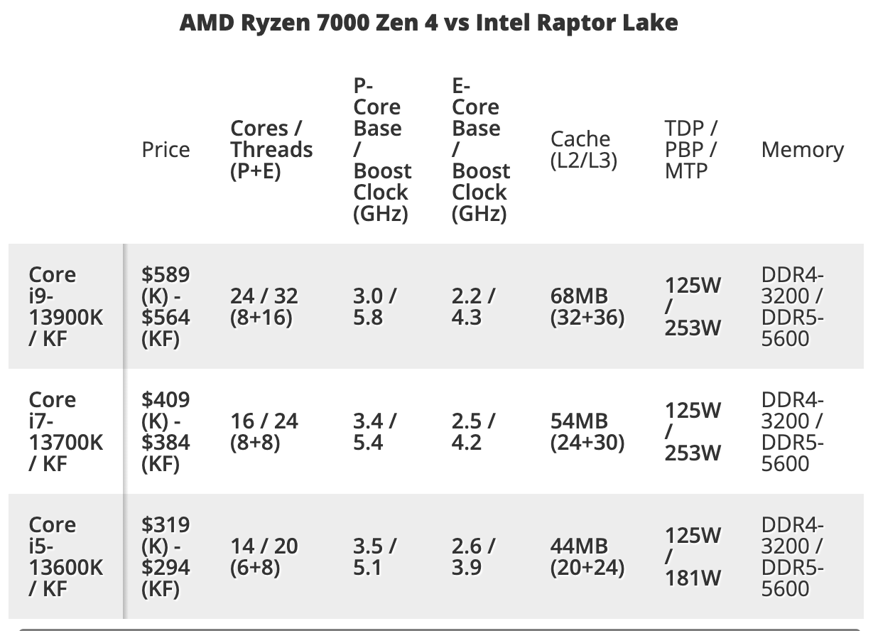
In practice, our computers’ physical memory (RAM) uses DRAM technology. We typically use 8 GB, 16 GB, and 32 GB in consumer grade PCs at the time this document is written (year 2023). Our CPU cache uses SRAM technology. We usually see the following specs when we shop for a CPU. The column “cache” refers to CPU cache which is commonly built using SRAMs.
Transistors Used
An SRAM cell requires 6 transistors to build (plus sense amps), while a DRAM cell requires 1 transistor + 1 capacitor.
A D Flip-Flop uses 2 D-latches plus an inverter. Assume that we can build a D-latch using 1 multiplexer (consisted of 4 NAND gates), and each NAND gate requires 4 transistors to build. This makes the transistor count to build a 1-bit DFF at 34 transistors.
The number of transistors used affects the cost of each memory unit greatly.
Tertiary Storage
Disk, NAND Flash or NOR Flash (SSD) are types of tertiary storage units. Unlike SRAMs, DRAMs, and DFFs, are non volatile, meaning that they are able to retain data even without being plugged to a power source. The details about tertiary storage units is out of syllabus. You can read the Appendix to seek further information if you’re interested.
Memory Addressing
This section refers to how bytes are addressed in the Main Memory (Physical Memory/RAM) and not on disk.
In practice, billions of DRAM cells are assembled together to form a large memory unit up to Terabytes in size. Each byte (8 cells) has a specific address. This analogous to a large apartment building with many fixed-size units within it, and each unit is assigned an address. The CPU will supply a memory address to read from or write to in each clock cycle.
Decoding
To decode an address, we can split the address into higher N address bits (selecting one of the rows) and lower M address bits (selecting a group of the columns), then read the information out of the bitlines as shown in the figure:

We often read hundreds of bits in parallel as there may be more than 1 CPU core in the system that can request a multitude of memory access operations simultaneously. For example, one row might contains hundreds of bit lines, and the lower M address bits will select which of group of 32 bits (or 64 bits, depending on the ISA) we want to read.
The Memory Hierarchy Idea
Since what we want is a large, fast, and cheap memory system: that is to perform with SRAM speed at the cost of a disk; we need to use a hierarchy of memory technologies to give the illusion of the perfect Physical Memory Unit. The principle is simple:
- Keep the most often used data at a small special device made of expensive SRAMs. We know this unit as the CPU cache. They’re usually assembled very near to the processor core, and is considered part of the CPU.
- As much as possible, the CPU should refer to the physical memory (DRAM) rarely. The physical memory is often refered to as main memory or simply “RAM”.
- Refer to disk (secondary storage) even more rarely.
As illustrated in the figure below, our computing device in practice is consisted not only of CPU and RAM, but also cache and disk (and later on I/O devices).

Cache is actually part of the CPU. The illustration above is just exaggerated to illustrate the hierarchy of memory devices.
The Locality of Reference
It is possible to give the user an illusion that they’re running at SRAM speed at most times due to the locality of reference.
Locality of Reference
The locality of reference states that reference to memory location \(X\) at time \(t\) implies that reference to \(X+\Delta X\) at \(t + \Delta t\) becomes more probable as \(\Delta X, \Delta t\) approaches zero.
In laymen terms, it means that there exists the tendency of a CPU to access the same set of memory locations repetitively over a short period of time.
Evidence that memory reference patterns exhibit locality of reference:
- Local stack frame grows nearby to one another.
- Related program instructions are near one another
- Data (e.g: arrays) are also nearby one another
There are two main types of locality:
- Temporal Locality: when a program accesses the same memory location multiple times within a short time span
- Cache memory exploits this by keeping recently accessed data available for quick reuse
- Spatial Locality: when a program accesses memory locations that are physically close to each other, such as elements in an array accessed sequentially
- Caches take advantage of this by fetching and storing blocks of memory, so nearby addresses are already loaded when needed.
We will learn more about this in the next chapter.
The Cache Idea
Here we discuss the first component of our memory hierachy: the cache.
CPU Cache
The cache is a small storage device assembled close to a processor core within a CPU. It contains temporary copies of selected memory addresses
Aand their contentMem[A]. The CPU now will always look for the requested instruction or data on the cache first, before starting to look for it in the physical memory in the event of cacheMISS.
The cache principles work as follows:
- Upon any instruction fetch, or instructions that involves LD or ST, CPU will first look for requested data in the cache
- If the information is found in the cache, return the content to CPU. This event is called a cache
HIT. - Otherwise this is the case of cache
MISS.
In the event of cache MISS:
- We look for the requested content in the physical memory (RAM)
- Once the content is found, replace the some (unused) cache content with this new content
In the event that the content is also not found in the RAM, we look for the content in the swap space region of the disk, and perform necessary updates on both physical memory and cache.
The Swap Space
A swap space is a dedicated unused space on the disk that is set aside to serve as an (virtual) extension of the RAM. We will learn more about this in the next chapter. This is the reason why it is important to not utilise your disk fully and set aside a few Gigabytes of “free” space so that your computing devices do not throttle when running extensive applications.
Average Access Time
The average time-taken (\(t_{\text{ave}}\)) to access a particular content in a system with a cache and a physical memory is:
\[\begin{aligned} t_{\text{ave}} &= \alpha t_c + (1-\alpha) (t_c + t_m) \\ &= t_c + (1-\alpha) t_m \end{aligned}\]where:
- \(\alpha\) is cache hit ratio (count of requests with a
HIT/ total request count), - \(t_c\) is cache access time, and
- \(t_m\) is physical memory access time
Think!
You easily simply extend the formula to incorporate the events where disk is used.
Think Further
The above cache principles are very simplified and incomplete. It does not address more details such as how can we store data in the cache, what to do in the event of cache miss in more detail, what happens when the physical memory itself is full, etc. We will perfect the cache principle to form what we call the caching algorithm in the next lesson.
Most modern CPUs have at least three independent caches:
- An instruction cache to speed up executable instruction fetch,
- A data cache to speed up data fetch and store, and
- A Translation Lookaside Buffer (TLB) used to speed up virtual-to-physical address translation for both (executable) instructions and data.
Data cache is usually organized as a hierarchy of more cache levels (L1, L2, L3, L4, etc.). In this course, we simplify some things and assume that there’s only one cache for both instructions and data, and one level of cache. We will learn more about TLB in the next chapter.
Types of Cache Design
There are two flavours in cache design: the fully associative (FA) cache and the direct mapped (DM) cache. Each design has its own benefits and drawbacks.
Fully Associative Cache (FA)
The FA cache has the following generic structure:

TAG and DATA are made of SRAM cells:
TAGcontains all bits of addressA.DATAcontains all bits ofMem[A].
For \(\beta\) CPU, we have 32 bits of TAG and 32 bits of DATA. Note the presence of a device called the tristate buffer. Refer to the appendix if you’d like to find out more.
Characteristics of FA cache are as follows:
- Expensive, made up of SRAMS for both
TAGandData(content) field (i.e: 64 bits in total for \(\beta\)) and lots of other hardware:- Bitwise comparator at each cache line (i.e: an “entry”:
TAG-Content, illustrated as a row in the figure above). - Tristate buffer required at each cache line
- Large
ORgate to computeHIT
- Bitwise comparator at each cache line (i.e: an “entry”:
- Very fast, it does parallel lookup when given an incoming address:
- Comparison between incoming address and all
TAGin each cache line happens simultaneously.
- Comparison between incoming address and all
- Flexible because memory address
A+ its contentMem[A]can be copied and stored on any cache line:TAG-Contententry.
FA cache is often used as the gold standard on how well a cache should perform. Any other cache designs will always compare its performance with the FA cache to gauge how good that new design is.
Direct Mapped Cache (DM)
The DM cache has the following generic structure:

Notice the 00 omitted at the back. This is because we are using byte addressing. In byte addressing, the last two bits are always 00 and carries no information. Therefore they shouldn’t be used as part of the k bits in the DM cache.
DM vs FA Cache
Characteristics of DM cache (in comparison to FA cache) are:
- Cheaper: less SRAM is used as the
TAGfield contains only the T-upper bits of addressA.- Also less of other hardwares: only 1 bit-wise comparator (to compare T-bits) needed.
- But we need K-bits selector Decoder to address each cache line and activate its word line.
- Not that flexible: A unique combination of K-bits of
Ais mapped to exactly one of the entries / row of DM cache. Each cache line in DM cache is addressable by the lowerK-bits of the address. The lower K-bits ofAdecides which cache line of DM cache we are looking for.- The number of entries in the DM cache is depends on the value of
K. - The DM cache is able to store up to \(2^K\)
TAG-Contententries. - The
Contentfield contains a copy of all bits of data atMem[A].
- The number of entries in the DM cache is depends on the value of
- Contention problem: DM cache suffers contention (collision problem) due to the way it strictly maps the lower
Kaddress bits to each cache line:- Two or more different addresses
A1andA2can be mapped to the same cache line if both have the same lowerKbits. - The choice of using
K-lower bits for DM cache mapping is better than using the upperTbits due to locality of reference, but it does not completely eliminate contention.
- Two or more different addresses
- Slower: There’s no parallel searching:
- At first, DM cache has to decode the K-bit address to find the correct cache line:
TAG-Contententry. - Then, perform comparison with between
TAGand the upper T-bit address input.
- At first, DM cache has to decode the K-bit address to find the correct cache line:
Summary
You may want to watch the post lecture videos here.
In this chapter, we are given a glimpse of various memory technology: from slowest to fastest, cheapest to the most expensive.
We use a hierarchy of memory technology in our computer system to give it an illusion that it is running at a high (SRAM level) speed at the size and cost of a Disk. The idea is to use a small, but fast (and expensive) device made of SRAMs to cache most recently and frequently used information, and refer to the physical memory or disk as rarely as possible. The memory hierarchy idea is possible only because the locality of reference allows us to predict and keep a small copy of recently used instruction and data in cache.
Here are the key concepts from this notes:
- Levels of Memory: these memory devices form the memory hierarchy.
- Registers: The fastest and most expensive type of memory, located within the CPU itself, used for immediate operations.
- Cache Memory: Slightly slower than registers, cache is also more expensive than main memory but offers faster access to frequently used data through techniques like L1, L2, and L3 caches.
- Main Memory (RAM): Provides larger storage capacity at lower speed and cost compared to cache. It is the main area where program applications and data in current use are kept so that they can be quickly reached by the CPU’s operations.
- Secondary Storage: Includes devices like hard drives and SSDs, which provide substantial storage capacity at much lower costs and slower access times compared to RAM.
- Locality of Reference: Utilizes the principle that programs tend to access a relatively small portion of their address space at any instant in time. This can be spatial, where data close to recently accessed data is accessed soon, or temporal, where recently accessed data is likely to be accessed again soon. This principle allows us to cache (e.g: recently used data) for faster performance.
- Performance Implications: The memory hierarchy is designed to provide the CPU with the fastest possible access to data. The efficiency of memory hierarchy affects the overall performance of computing systems, as faster data access times can significantly enhance the speed at which programs execute.
- Cache access time: Computed as follows, (hit rate * cache access time + miss rate * (cache + memory access time)). Remember that in the event of a MISS, we would’ve already checked the cache (to know that it’s a MISS).
- Common Cache Designs, FA and DM: The FA cache is the gold standard of cache, while the DM cache is a cheaper cache design but suffers contention, resulting in a lower performance as compared to the FA cache.
By understanding the structure and function of the memory hierarchy, systems can be designed to efficiently handle varied process demands, improving both the speed and performance of computer systems.
Appendix
Disk
A disk (also known as Hard Disk Drive) is an old-school mechanical data storage device. Data is typically written onto a round, spinning aluminum that’s been coated with magnetic material that we call a “disk”. Several of these round platters are put together on a shaft, and they make up a cylinder. The cylinders are able to spin at around 7000 revolutions per minute.
Each round disk can be separated into concentric circles sections we call track, and each track can be further separated into sectors as shown below. Each sector contains a fixed number of bits.

A disk is able to retain its information even after they’re not directly plugged to power supply anymore. Therefore, unlike Register, SRAM, and DRAM that are volatile, a disk is a type of low-power and non-volatile storage device. Non-volatile memory that relies on mechanism such magnetic field changes to encode information takes far longer to change its values.
To Write and Read to Disk
To perform a read or write to a disk, the device has to mechanically move the head of the disk and access a particular sector. This takes up a lot of time, and thus resulting in large latency for both read and write.
The writing is done by a magnetic head, mounted at the end of an actuator arm that pivots in such a way that the head can be positioned over any part of the platter. The same head may also read the stored data. Each platter has its own read and write head, but all heads are mounted on a common arm assembly.
Accessing Data on Disk
The CPU itself cannot directly address anything on a disk, therefore any data/instruction that the CPU needs to access must be migrated (copied over) from Disk to RAM/Physical Memory first before the CPU can do anything with it.
To access any data on disk, the CPU has to first give the command for a chosen block of data from some sectors to be copied into the RAM. After the entire block of data is in the RAM, then the CPU can start accessing the specific 32-bit data (or n bits, depending on the architecture).
Unlike in a RAM, we typically cannot just read a single word of data from the Disk. We need to migrate a whole sector. This is reasonable in practice since we rarely just need only single word of data. We typically need a whole sector of data to run our applications. You may watch this animated video to understand how disk works better.
Addressing Data on Disk
In short, data addressing on disk does not work the same way like how we address data in RAM / Physical Memory. The details on how data is addressed and stored on disk is out of our syllabus. It highly depends on the Operating System and disk format (e.g: NTFS, APFS, etc). If you’re curious, you may read further details here on how UNIX system stores data on disk.
If you have the time and are interested about how data is managed and stored on non-volatile storage devices, you can give this video a watch and follow the series of lectures.
Other non-volatile storage device: NAND Flash and NOR flash
This section is out of syllabus, but created for the sake of knowledge completeness since flash drive is the dominant technology at the time this article is written in 2023. You may watch this wonderful animated video to find out how SSDs which uses flash-drive technology work to store your data before reading the summary in this section.
There’s one other commonly used non-volatile memory that we can use as storage with faster read/write operation in general. We commonly know this as the Solid-State Drive (SSD). An SSD is more expensive than a plain old HDD of the same size.
SSDs use a type of memory chip called NAND flash memory. NAND devices store a small amount of electrical charge on a floating gate when the cell is programmed. Its cell has very high resistance, and its capacitance can hold a charge for a long period of time. However, unlike in a DRAM-based memory, we cannot change one cell value quickly at a time in a flash memory.
NOR Flash is another alternative which offers a much faster read speed and random-access capabilities, making it suitable for storing and executing code in devices such as cell phones. NAND Flash offers high storage density and a smaller cell sizes and is comparably lower in cost. Hence NAND is often preferred for file storage in consumer applications.
To change its values, we need to reset and rewrite an entire large block at once, which is a much slower process for a write as compared to a RAM. The charge stored in the NAND flash can still fade over time if we never power it back up anymore. Therefore it is important to power the flash storage from time to time to retain its data. If you’re curious you can read more about how HDD and SSD work here to understand how each of the work and the pros and cons of each device.
Memory Addressing
This section refers to how bytes are addressed in the Main Memory (Physical Memory/RAM) and not on disk.
In practice, billions of DRAM cells are assembled together to form a large memory unit up to Terabytes in size. Each byte (8 cells) has a specific address. This analogous to a large apartment building with many fixed-size units within it, and each unit is assigned an address. The CPU will supply a memory address to read from or write to in each clock cycle.
Decoding
To decode an address, we can split the address into higher N address bits (selecting one of the rows) and lower M address bits (selecting a group of the columns), then read the information out of the bitlines as shown in the figure:
We often read hundreds of bits in parallel as there may be more than 1 CPU core in the system that can request a multitude of memory access operations simultaneously. For example, one row might contains hundreds of bit lines, and the lower M address bits will select which of group of 32 bits (or 64 bits, depending on the ISA) we want to read.
Tristate Buffer
 A tristate buffer, also known as a three-state buffer, is an electronic circuit component that is used to control data flow on a bus or between circuit components. It can operate in three different states:
- Output High: The buffer outputs a high voltage level, representing a binary ‘1’.
- Output Low: The buffer outputs a low voltage level, representing a binary ‘0’.
- High Impedance (High-Z): The buffer is effectively disconnected from the circuit, neither outputting nor sinking current. This state allows other devices to drive the line without interference from the buffer.
The primary function of a tristate buffer is to allow multiple circuits to share a single output line or data bus without connecting their outputs together at the same time, which could cause conflicts or damage. This is crucial in digital electronics, particularly in systems where bus architectures are used, allowing only one device to speak at a time while others remain silent. The use of tristate buffers helps in reducing power consumption and avoiding signal contention on shared lines.
It has the following truth-table:
High impedance
High impedance (or High-Z) is a state when the output is not driven by any of the input(s). We can equivalently say that the output is neither high (1) nor low (0) and is electrically disconnected from the circuit.