 50.002 CS
- Objectives
- Submission
- Starter Code
- Related Class Materials
- Introduction to FPGA Development
- Basic FPGA Development using Alchitry Labs V2
- Module
- Simulation
- Value assignment
- Inputs, Interactivity, and Bit-Flow
- Static Discipline in Practice
- Internal
sig - Array Duplication, Builder, and Concatenation
- Auto Truncation, Auto Extension, and Width Mismatches
- Digging Deeper into the Always Block
- A Caveat: Evaluation Order
- Summary
50.002 Computation Structures
Information Systems Technology and Design
Singapore University of Technology and Design
Lab 1: Digital Abstraction with Hardware Design Language
Objectives
By the end of this lab, you should be able to:
- Understand that HDL does not describe instructions running in time, it describes physical connections that exist in parallel
- Recognise that every signal is a wire or bundle of wires, and every assignment is a bit pattern placed onto real hardware
- Interpret and control bit-width and base notation correctly when assigning values
- Use Alchitry Labs V2 to create a project and run a simulation for an FPGA design
- Identify input and output ports and understand how constraint files map them to physical pins
- Explain why every output must be driven and why undriven or floating signals are illegal
- Distinguish combinational behaviour from accidental memory inference
- Apply simple bitwise logic (AND, OR, XOR) and read its truth-table meaning
- Reason about static discipline: valid inputs must always produce valid, determined outputs
- Build intuition for bit flow from inputs through logic to outputs
Submission
There’s no code submission/checkoffs for this lab. Simply complete the Lab Questionnaire (2%) on eDimension.
Starter Code
There’s no starter code for this lab. You simply need to have Alchitry Labs V2 installed. You don’t need Vivado for this lab, we are only going to run simulations.
Consult FPGA resources listed here before coming to the lab or after the lab to enhance your knowledge on FPGA programming in general. This will greatly accelerate the quality of your 1D & 2D project.
Related Class Materials
The lecture notes on digital abstraction and basics of information are closely related to this lab.
| Lecture notes topic | Lab 1 part |
|---|---|
| Number systems: binary, decimal, octal, hex (Basics of Information) | Using 8b00001010, 8h0A, 8d10 to describe the same 8 bit pattern that drives LEDs |
| Bits as encodings, not just numbers (Basics of Information) | Treating each switch and LED as one encoded bit; viewing a row of switches or LEDs as a fixed length code word (number, character, choice) |
| Basic logic gates and Boolean operations AND, OR, XOR, NOT, BUFFER (Basics of Information) | Using bitwise &, |, ^, ! on io_dip to implement gate truth tables and see them on real LEDs |
| Analog to digital abstraction via voltage thresholds (Digital Abstraction) | Treating every wire in the simulator as carrying a logical 0 or 1 while ignoring the analog details |
| Static discipline: valid inputs yield valid outputs when every block obeys the voltage contract (Digital Abstraction) | Ensuring every sig and output is driven for all input patterns in always; avoiding floating signals and unintended inferred memory |
| Combinational device definition: outputs depend only on current inputs (Digital Abstraction) | Using always blocks to describe combinational behaviour where outputs are fully specified for every input and never depend on past values |
Introduction to FPGA Development
In this lab, we’ll explore basics of HDL for FPGA Development. This is crucial for your 1D project, where you’re tasked to create an electronic hardware prototype from combinational and sequential logic components using FPGA. It is a culminating project that integrates and applies the knowledge and skills you learn in 50002 because you are not coding on a computer, you are building the digital system that a computer is made of.
What are we doing here? (Long Version)
Remember the purpose of learning 50.002? To understand how computers work from transistors into operating system. That is, to know how to build a computer, from literal scratch. A computer is not just our general purpose controller, it can be simple stuffs like microcontroller or logic boards inside your oven, washing machine, air conditioner, etc. When we understand how the general-purpose one works, it’s pretty intuitive how other specific types work too.
Anyway, we shall highlight that we are NOT talking about: buying CPU, motherboard, GPU, RAM and then plugging things in together and calling that “building”. We meant literally making one from transistors, like this one (you are looking at a 4-bit computer from this amazing tutorial):
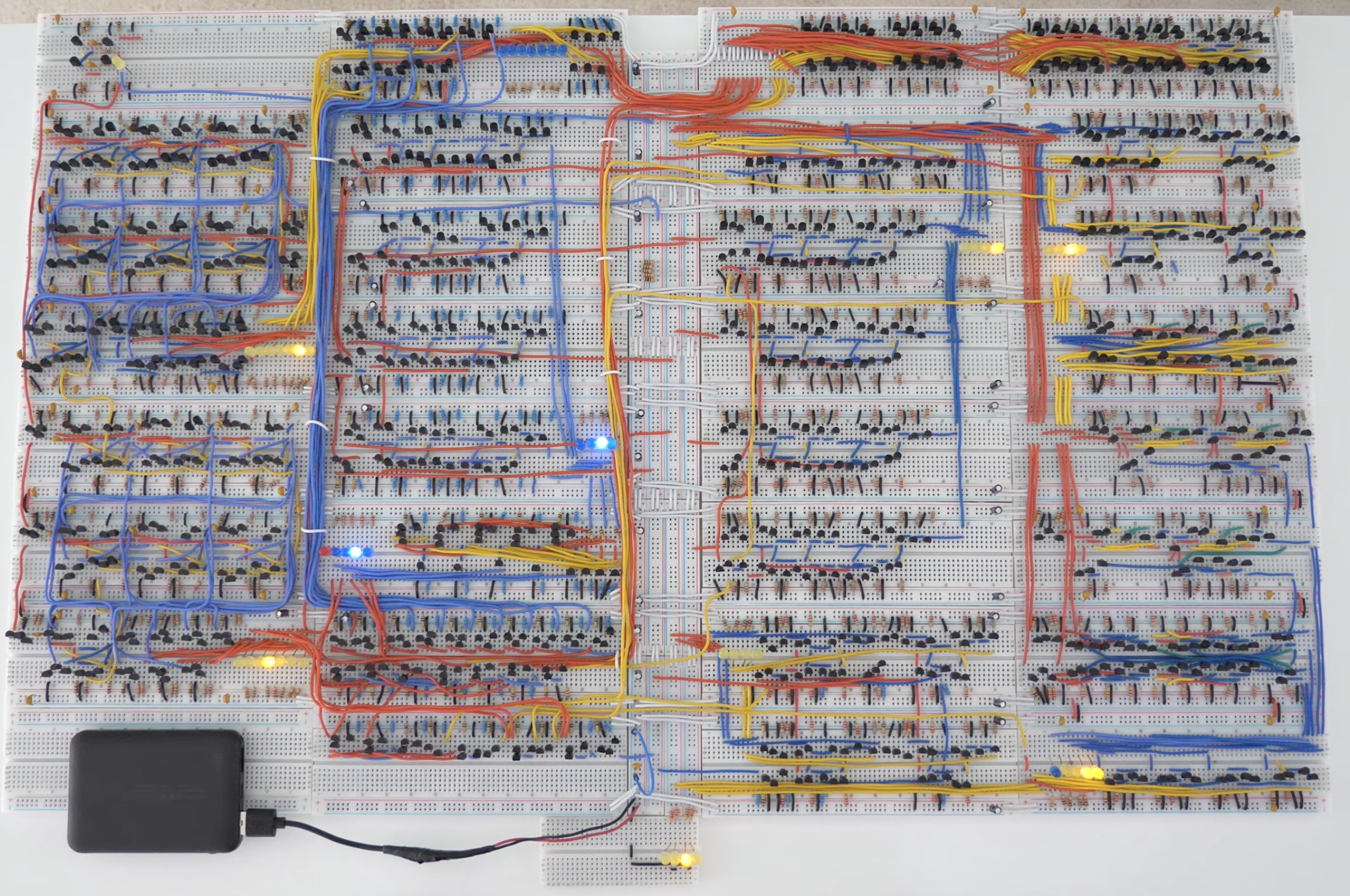
When you build the above, you are not coding an application. You are building the machine that will run code and make coding possible. That is a general purpose computer, not “arithmetic purpose computer”, or “counting machine purpose computer”, but GENERAL.
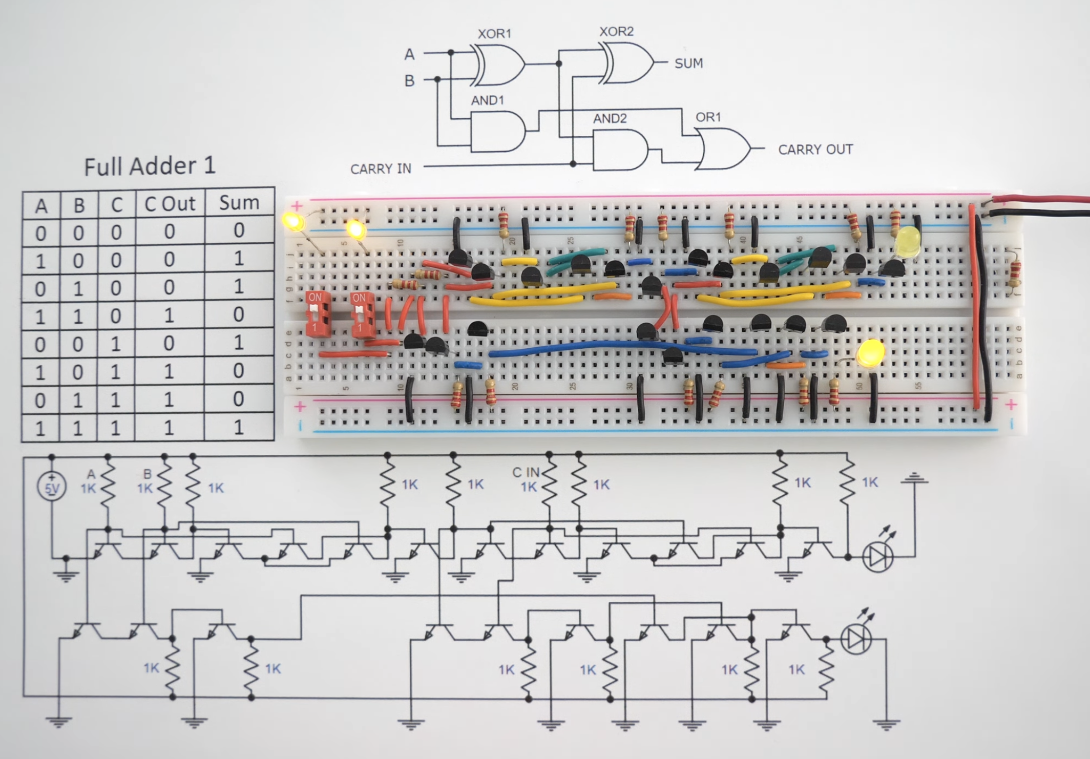
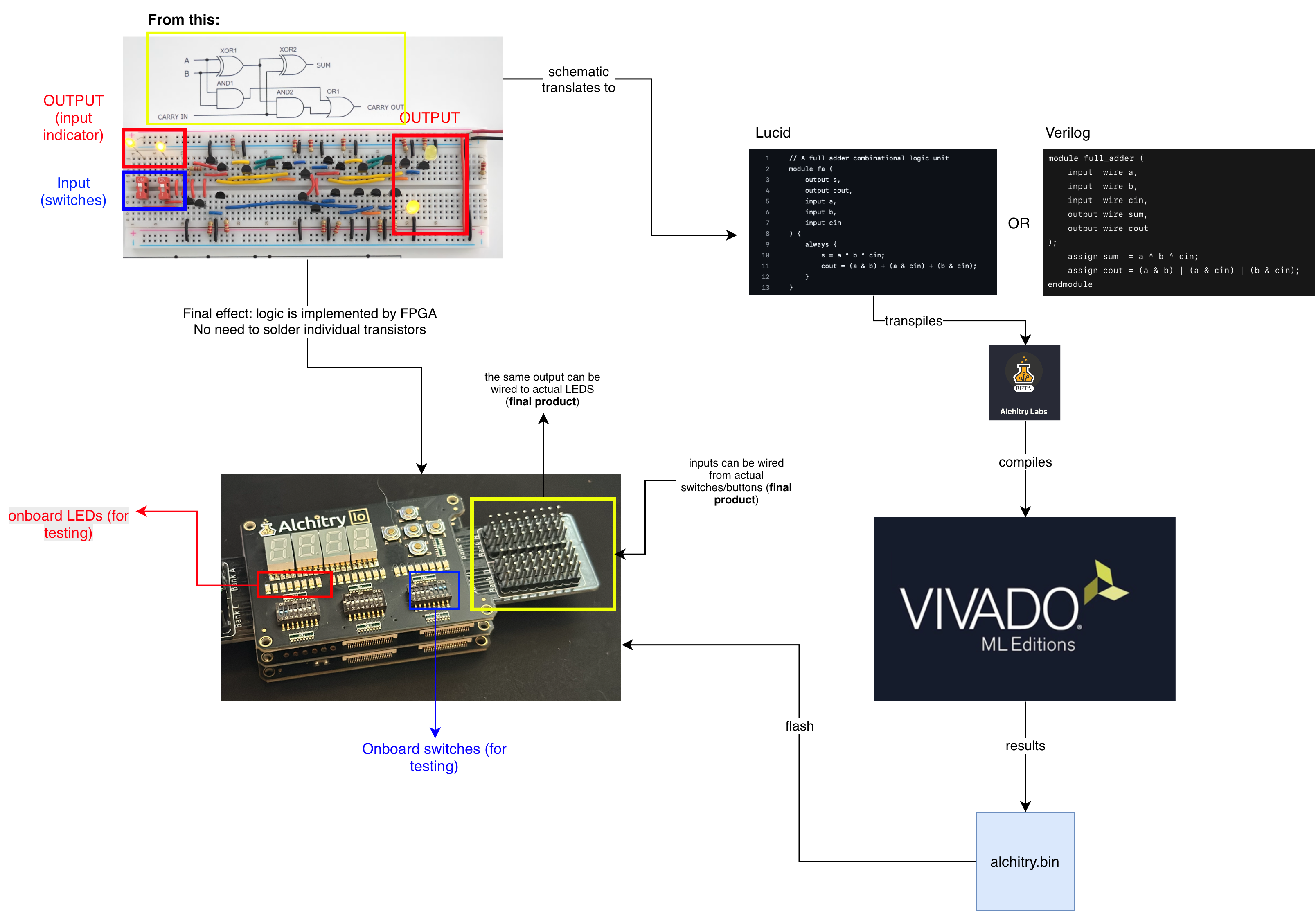
Let’s tie it back to the lecture materials. In lecture you saw digital abstraction and basic logic gates. We treat messy analog voltages as clean 0 or 1 which we call a bit, and we combine ideal gates to build adders and other digital systems. On real hardware those gates are built from MOSFETs (transistors) and wired together on a breadboard or PCB. We can come up with theoretical schematics of digital devices, like the following (1-bit adder) which is a crucial part of a logic unit in many computers (computers compute):
![]()
But in order to test whether it works, we need to physically wire things together, then connect some LEDs to see “output” and some buttons and/or switches to type “inputs”, like so (image taken from this tutorial):
That approach is fine for a demo, but it quickly becomes painful when we bring it to production/testing level.
- We need to test if our schematic works in real life (does it overheat? is it too slow?)
- Then we need to iteratively improve it: come up with new design, new connections
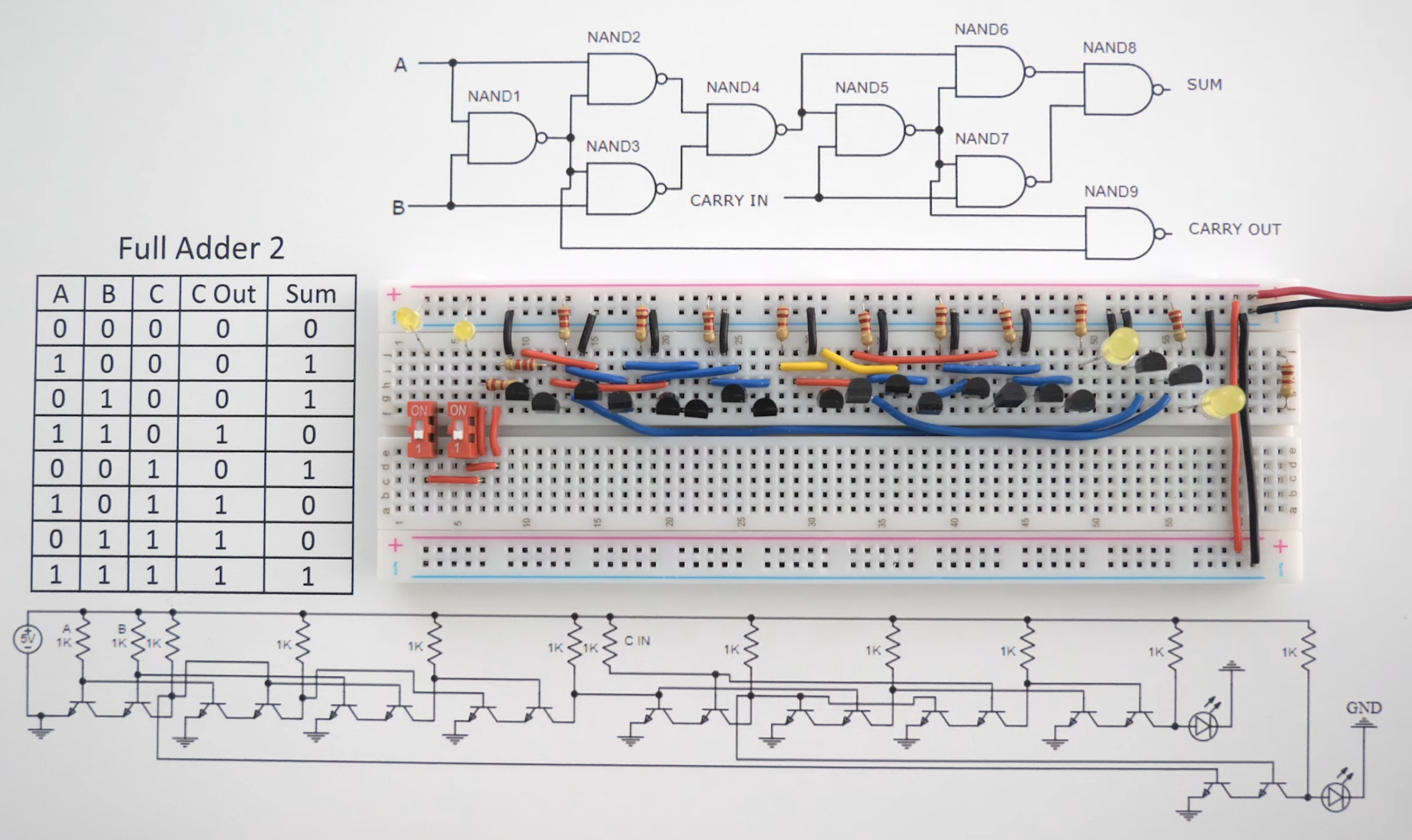
Every change in the design means real physical work (resoldering, change connections, adding/removing wires, etc) and is prone to bugs. You need to realise that people do not come up with design schematics in one sitting. They require many iterations, just like coding and designing the right app. The following image shows an alternative design of the adder:
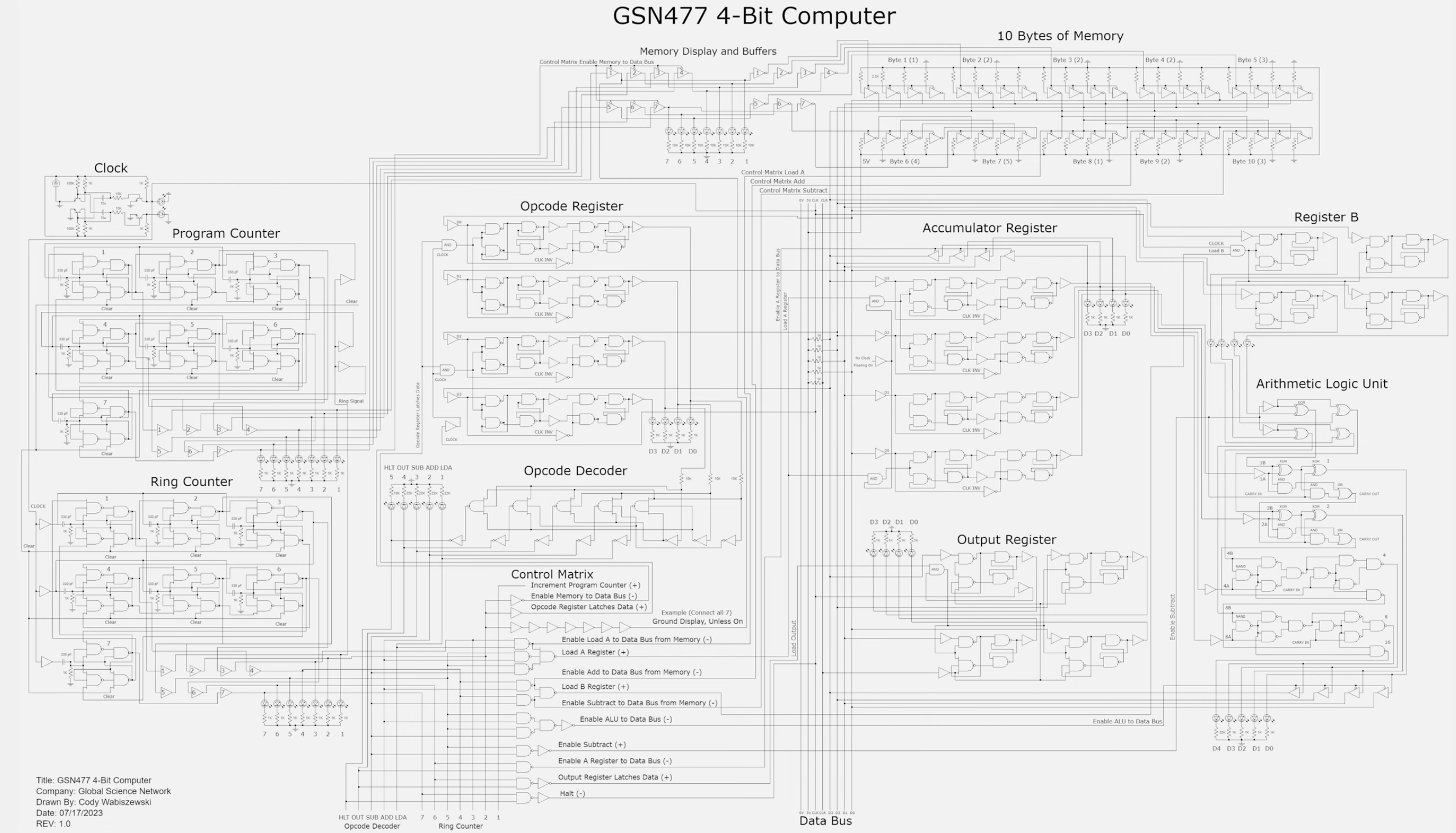
It becomes more obvious with complex system. The schematic of the following 4-bit computer has surely undergone numerous iterations of implementation-testing cycle:
You get the idea, you can’t design digital circuits of a large scale on a breadboard and iteratively improve your design.
So this is where FPGA comes into play: it can be programmed to behave like certain digital circuits. But first you need to describe how your circuit looks like (which module is connected to which, how many output/input etc).
Just like “coding”
When you have a concept and try to materialise it by writing a few lines of Python, you simply type then run the program, see the output, and tweak it until it works.
In digital circuit design (making a computer), you are doing the same thing, except instead of writing software, you are designing a digital circuit. Your code is no longer just instructions for a CPU, it is a description of gates, wires, and connections.
Without an FPGA, this would mean soldering MOSFETs and rewiring breadboards for every change. The FPGA removes that friction, so you can iterate on circuit design as easily as you iterate on code.
What are we doing here? (Short Version)
In this lab you will:
- Treat HDL as a hardware wiring description, not a step-by-step program.
- Practice controlling bit-width and base notation when driving LEDs.
- Add IO Shield ports via the constraint file and ensure every output is driven.
- Use
always { ... }to describe combinational logic that is always active. - Avoid incomplete assignments that create undefined signals and imply memory.
- Build intuition for bit flow: inputs (buttons/switches) map to output patterns (LEDs).
What FPGA Offers
Unlike software simulations, FPGAs let you directly program hardware, giving you a real-world, hands-on understanding of how digital systems work.
FPGAs offer:
- Flexibility: Easily reprogram and experiment with different designs.
- Real-time Feedback: See your circuits in action, running in parallel.
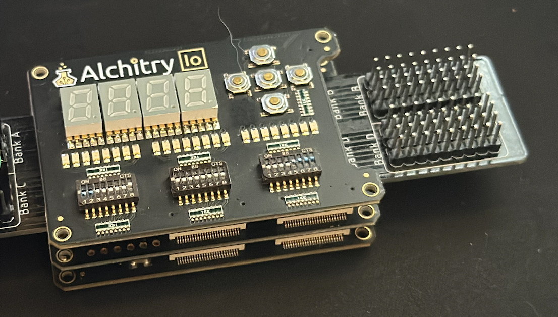
You will be given the Alchitry Au FPGA development kit as a group, which includes I/O ports for easy connections to external devices. It’s a cost-effective option compared to full-scale Xilinx boards, making it ideal for education.
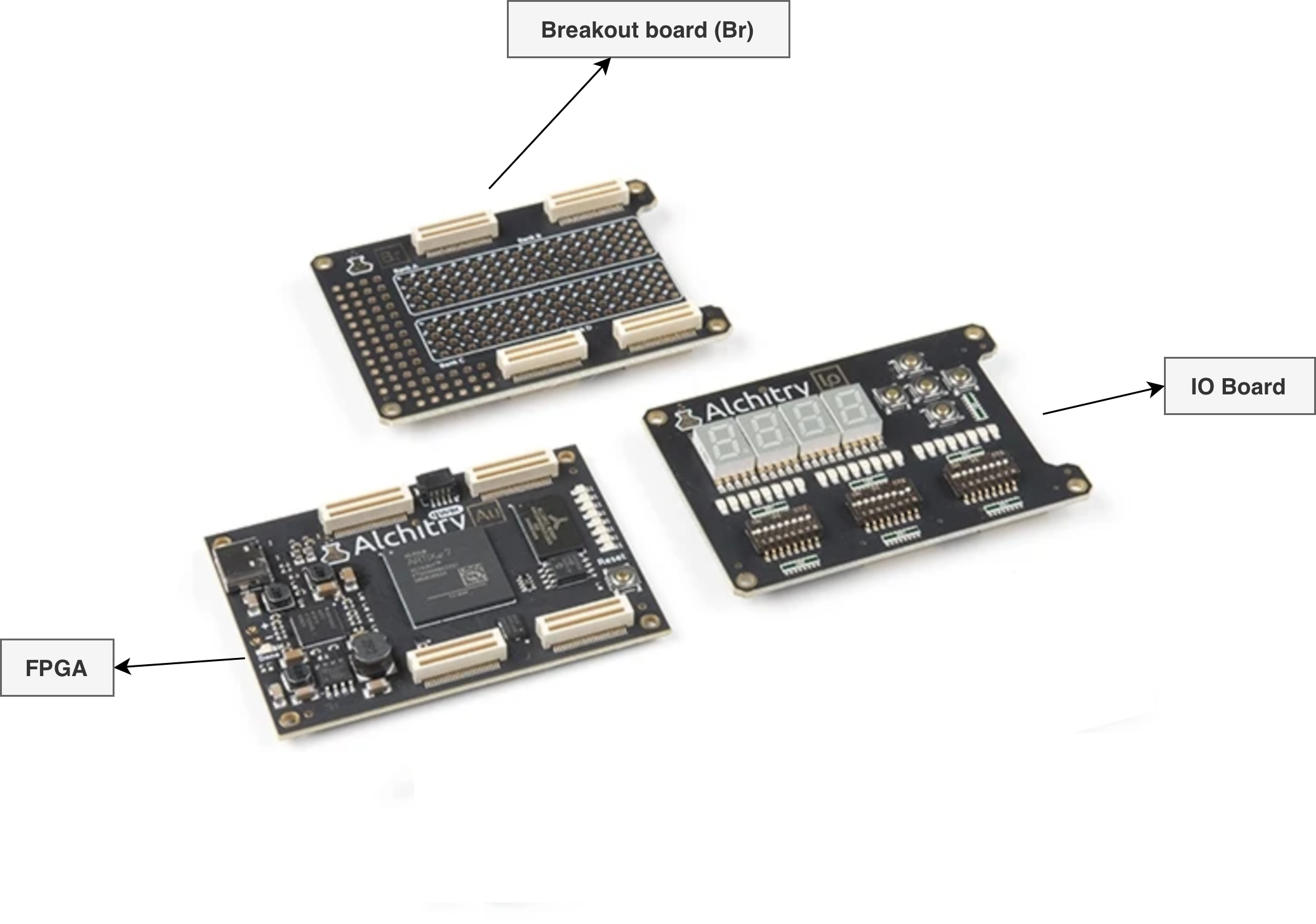
Together they will be stacked as such (the extra “wings” pinouts are custom-made):
To program the FPGA, we’ll use the Lucid V2 Hardware Description Language (HDL), which is simpler (in syntax) than traditional HDLs like Verilog, making it easier to learn. Alchitry Labs will be our development environment (IDE), converting Lucid into Verilog for synthesis in Vivado.
The entire pipeline is as follows:
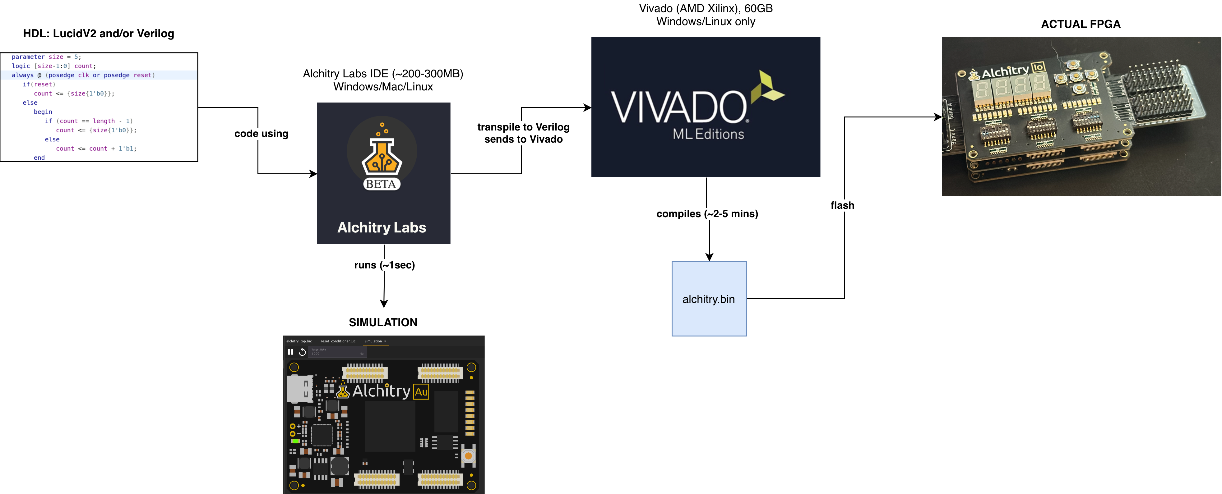
When you “program” an FPGA, you are configuring its logic cells and connections to implement your desired digital circuit or design. This is different from programming software, as you are actually defining hardware behavior within the FPGA.
Now you no longer have to solder individual transistors as the bulk of the logic can be implemented by the FPGA. You are left with just peripheral connections (I/O like buttons/switches/leds):
Why not Vivado + Verilog and skips Alchitry Labs altogether?
Vivado is the industry-standard tool for FPGAs. However, both Vivado and Verilog have steep learning curves, especially for beginners. It is not suitable for 50.002 because we need to cover a lot of foundational topics, ranging from MOSFETs and transistors to operating systems. Alchitry Labs, will handle the conversion to Verilog in the background, so you can focus on learning the core concepts without diving into the complexities of Verilog or Vivado.
Alchitry Au (Original)
The Alchitry Au FPGA development kit hardware given to you is the original version purchased prior to 2025, not the V2. Do not confuse this to the AlchitryLabs IDE version (V2) and Lucid version (also V2).
We are using Lucid V2 with Alchitry Labs V2 to code, + Vivado to compile the binary to be loaded to our Alchitry Au FPGA.
Prior to 2025, we were using Alchitry Labs 1.2.7 and Lucid V1. It worked well, but there’s no simulation so development is kind of rough. The V2 IDE supports simulation which improves the learning experience greatly.
Basic FPGA Development using Alchitry Labs V2
This section briefly explains how to install the necessary tools and basic Lucid V2 syntax. Lucid V2 is a great language to program simple behavior on the FPGA which is sufficient for this course.
You are strongly recommended to give the official reference guide a read. Bookmark it.
Installation
Install the IDE (Alchitry Labs V2). If you’re using macOS, you might need to manually override the security settings as indicated here.
You can write HDL program using Alchitry Labs using Lucid or Verilog and then run simulations. Once you’re happy with the simulation result, you can build the binary and load it to the FPGA hardware. This step requires installation of Vivado. Read this guide for more information. This is important for your 1D project but it is not required in this lab.
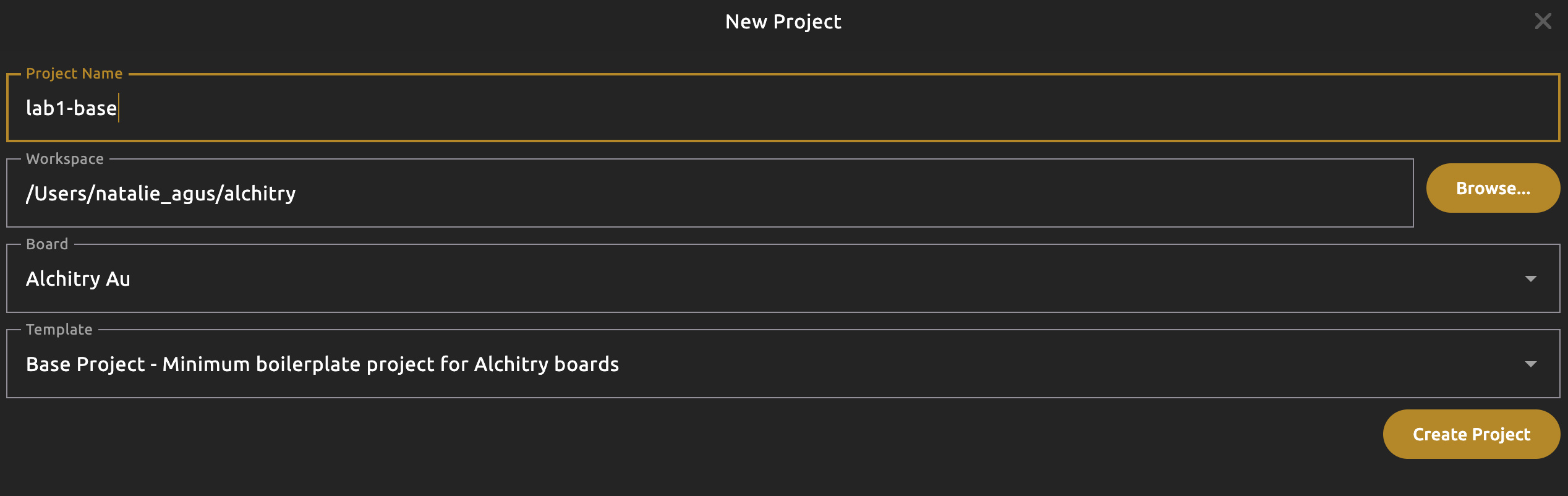
Create New Project
Create a new project with Base Project as a template. Choose Alchitry Au (not Alchitry Au V2). This is our FPGA development board.
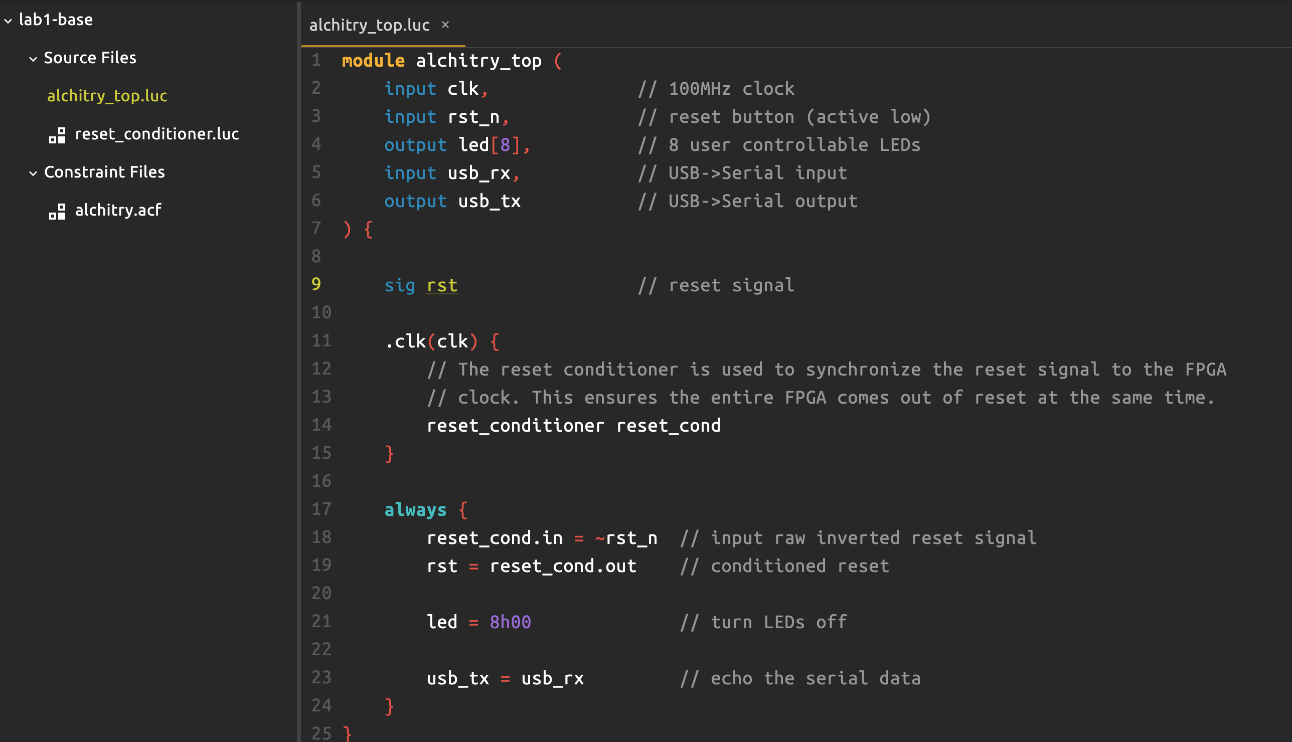
There are a few Lucid (.luc) source files created:
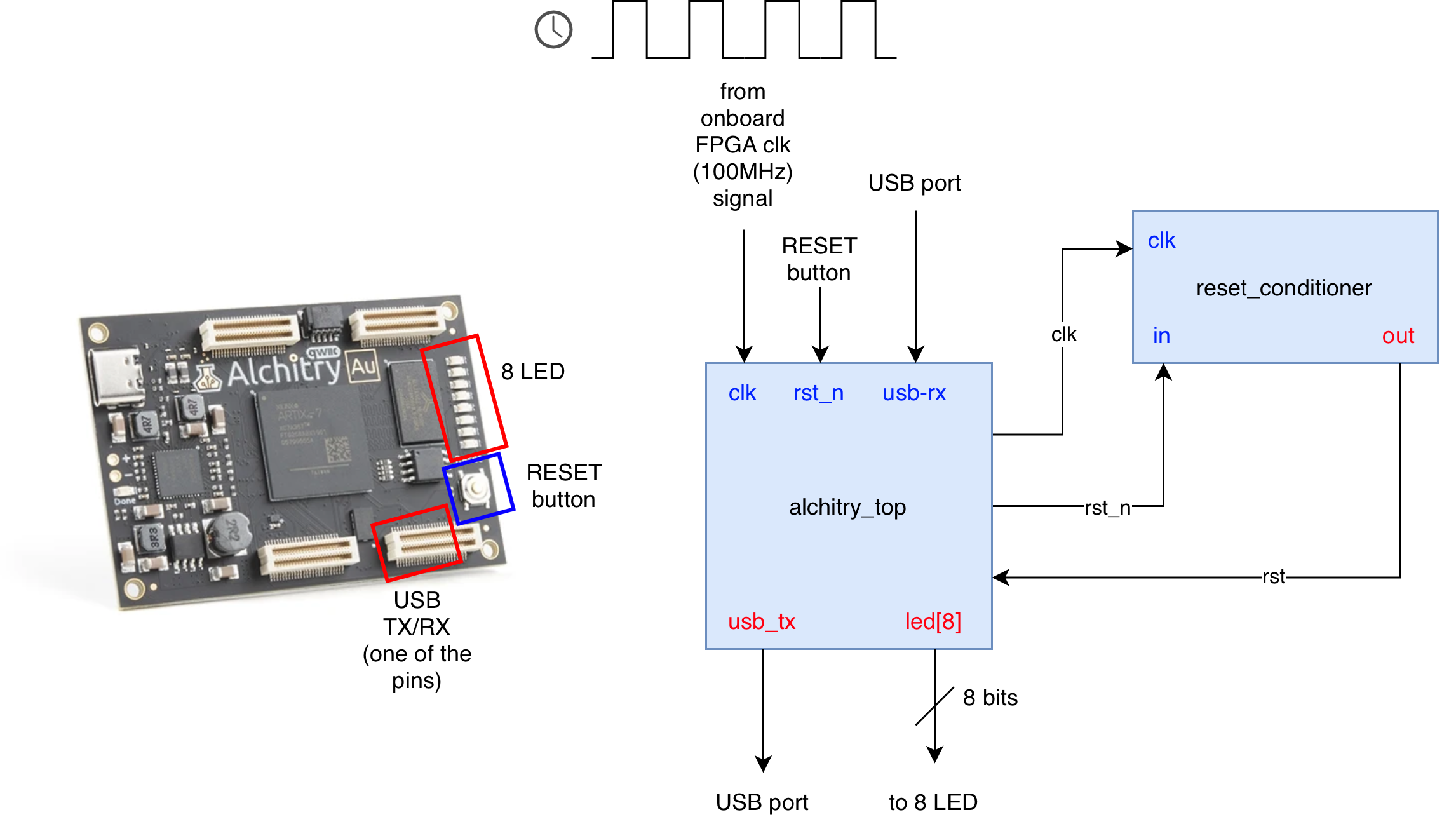
alchitry_top.luc: This is the top-level file, like a “main” file. It connects all submodules and interfaces with external I/O. The ports are defined in this top-level file, while the constraint file (.acf) maps them to physical FPGA pins.reset_conditioner.luc: this is a module obtained from Alchitry component library. It synchronizes the reset button so that all modules in the FPGA can receive the reset signal at the same time.Constraint files: alchitry.acf: a constraint file maps the FPGA I/O pin with a logical name that you can define inalchitry_top.luc, so that you can define the logic to control these I/Os.
Module
Modules are the core building blocks of any HDL project. They’re like “class” keyword in OOP. They encapsulate specific functionality, allowing you to design complex circuits by breaking them into smaller, manageable components. Each module can have parameters and ports that define how it interacts with other parts of the design. The general structure for a module declaration in Lucid is:
module module_name #(
    // optional parameter list
)(
    // port list
) {
    // module body
}
We will not touch parameter for now, that’s for the next lab.
By organizing your design into modules, you create reusable, testable blocks that can be combined to form larger systems.
The alchitry_top.luc module is one of the modules created in this base project template:
module alchitry_top (
    input clk,              // 100MHz clock
    input rst_n,            // reset button (active low)
    output led[8],          // 8 user controllable LEDs
    input usb_rx,           // USB->Serial input
    output usb_tx           // USB->Serial output
) {

    sig rst                 // reset signal

    .clk(clk) {
        // The reset conditioner is used to synchronize the reset signal to the FPGA
        // clock. This ensures the entire FPGA comes out of reset at the same time.
        reset_conditioner reset_cond
    }

    always {
        reset_cond.in = ~rst_n  // input raw inverted reset signal
        rst = reset_cond.out    // conditioned reset

        led = 8h00              // turn LEDs off

        usb_tx = usb_rx         // echo the serial data
    }
}
This is the main module, that interfaces between code (HDL) and hardware (physical pins) on the FPGA.
The alchitry_top module utilises the reset_conditioner module (open reset_conditioner.luc). Don’t worry if you don’t understand its syntax yet.
How are Modules Realised?
Modules take up FPGA components (called Logic Units or LUTs) when instantiated. LUTs in the FPGA will be used to behave like that module you instantiated. For instance, Alchitry Au FPGA has about 33,000 LUTs. If you instantiate 20 modules that utilises 400 logic units each. That means it will take up 8000 of your FPGA logic units.
Instantiating more modules or larger bit-width logic uses more of the FPGA’s resources and may hit a limit if your design grows large.
Port List
Each module should have a list of ports, that’s like the input and output of a “function”. They’re defined inside the brackets with keyword input and output. There are more port keywords, but we omit them for now.
In the alchitry_top module, we have 5 ports:
module alchitry_top (
    input clk,              // 100MHz clock
    input rst_n,            // reset button (active low)
    output led[8],          // 8 user controllable LEDs
    input usb_rx,           // USB->Serial input
    output usb_tx           // USB->Serial output
)
Inputs:
clk: 1 bit clock signal, which drives the timing of the module.- By default, the FPGA supplies 100MHz clock (defined in the constraint file
alchitry.acf) - You can change this value if your design fail to meet timings, e.g: 10MHz instead. The steps required are more involved, you can give this guide a read.
rst_n: 1 bit reset signal connected to the reset button of the FPGAusb_rx: serial input port of the FPGA (USBC)
Output:
led[8]: 8 bit output signal mapped to each of the 8 LED on the FPGAusb_tx: serial output port of the FPGA (USBC)

In the reset_conditioner module, we have 3 ports (2 inputs and 1 output)
module reset_conditioner #(
    STAGES = 4 : STAGES > 1 // number of stages
)(
    input clk,  // clock
    input in,   // async reset
    output out  // sync reset
)
Module Body
The module body defines connection and logic that exists in this module. It’s separated into two parts: instantiation and the always block.
Module Body: Module Instances
The next part of a module might contain instantiation of other modules that you might need. This is the heart of digital systems design: we connect smaller parts together to make bigger, more complex systems. Each part can communicate and understand each other’s signals because of static discipline.
Here we utilises another module called reset_conditioner (you can click on the file reset_conditioner.luc to see how it’s implemented, but it’s not important now)
    .clk(clk) {
        reset_conditioner reset_cond
    }
When we instantiate a module, we need to supply its inputs properly either in the instantiation or in the always block. reset_conditioner requires 1-bit clk signal, so we need to supply it as such. This is analogous to instantiation in Java or Python.
The syntax for instantiation and input connection can vary, depending on your preference:
    // block instantiation, any modules described inside the clause will receive 1-bit SIGNAL from this module connected to its `INP_PORT`
    // useful if you have a bunch of modules with similar input ports
    .INP_PORT(SIGNAL) {
        <module_type> <instance_name>
    }

    // regular instantiation with port setting
    <module_type> <instance_name>(.INP_PORT(SIGNAL),...)

    // regular instantiation without port setting
    <module_type> <instance_name>
.INP_PORT is the input port name of the module you are about to instantiate. SIGNAL is the signal name in this module that serves as an input to the module you’re instantiating.
We can instantiate reset_cond this way (mixed port setting):
    .clk(clk) {
        reset_conditioner reset_cond
    }


    always {
        reset_cond.in = ~rst_n

        ...
    }
or this way:
    reset_conditioner reset_cond


    always {
        reset_cond.clk = clk
        reset_cond.in = ~rst_n

        ...
    }
or this way:
    reset_conditioner reset_cond(.clk(clk), .in(~rst_n))


    always {
        ...
    }
or a mixture:
    .clk(clk) {
        reset_conditioner reset_cond(.in(~rst_n))
    }


    always {
        ...
    }
All four methods yield the same outcome, that is to define the same connection between reset_conditioner and alchitry_top module (like soldering wire connections). Rule of thumb: define connections during instantiation as much as possible (if it’s known since the beginning, not some intermediary sig) for neater code.
The following diagram shows the relationship between alchitry_top module and reset_conditioner module. Just like lego-pieces, each module can utilise other modules via instantiation and then you define the connections based on the port definition. The port names written in blue are inputs and the red ones represent outputs. The ones written in black are intermediary named signals, just like private attributes you’d define in a class.
Module Body: The always Block
The always block
In hardware description languages like Lucid, the
alwaysblock represents continuous and parallel execution, unlike traditional sequential programming where instructions are executed one after the other. It is used to define connections and relationships between different signals happening in parallel, rather than executing sequential instructions like in software programming.
So in other words, the always block in Lucid describes continuous combinational logic, not a step-by-step program. Everything inside it is interpreted as hardware that is always active, evaluating in parallel with the rest of the circuit.
Advanced note: that Lucid does not use Verilog-style sensitivity lists like @(*) or @(posedge clk). There is no posedge or negedge attached to an always block. Sequential behavior never comes from always itself. If this sentence makes no sense to you right now, it’s alright to move on. You will understand this more in the coming weeks when we study sequential logic.
In alchitry_top.luc, we have:
    always {
        reset_cond.in = ~rst_n  // input raw inverted reset signal
        rst = reset_cond.out    // conditioned reset

        led = 8h00              // turn LEDs off

        usb_tx = usb_rx         // echo the serial data
    }
It simply means: “continuously drive these signals with this logic.”
- Drive the input port of
reset_condmodule with the inverse ofrst_n - Drive
rstsignal with the output ofreset_condmodule - Drive
ledsignal (8bit) with 0s (low voltage) - Drive
usb_txwithusb_rx
The hardware representation of the connections described in this always block is:
No Storage
An always block by itself produces no storage. It like a plain and simple wire connections.
Simulation
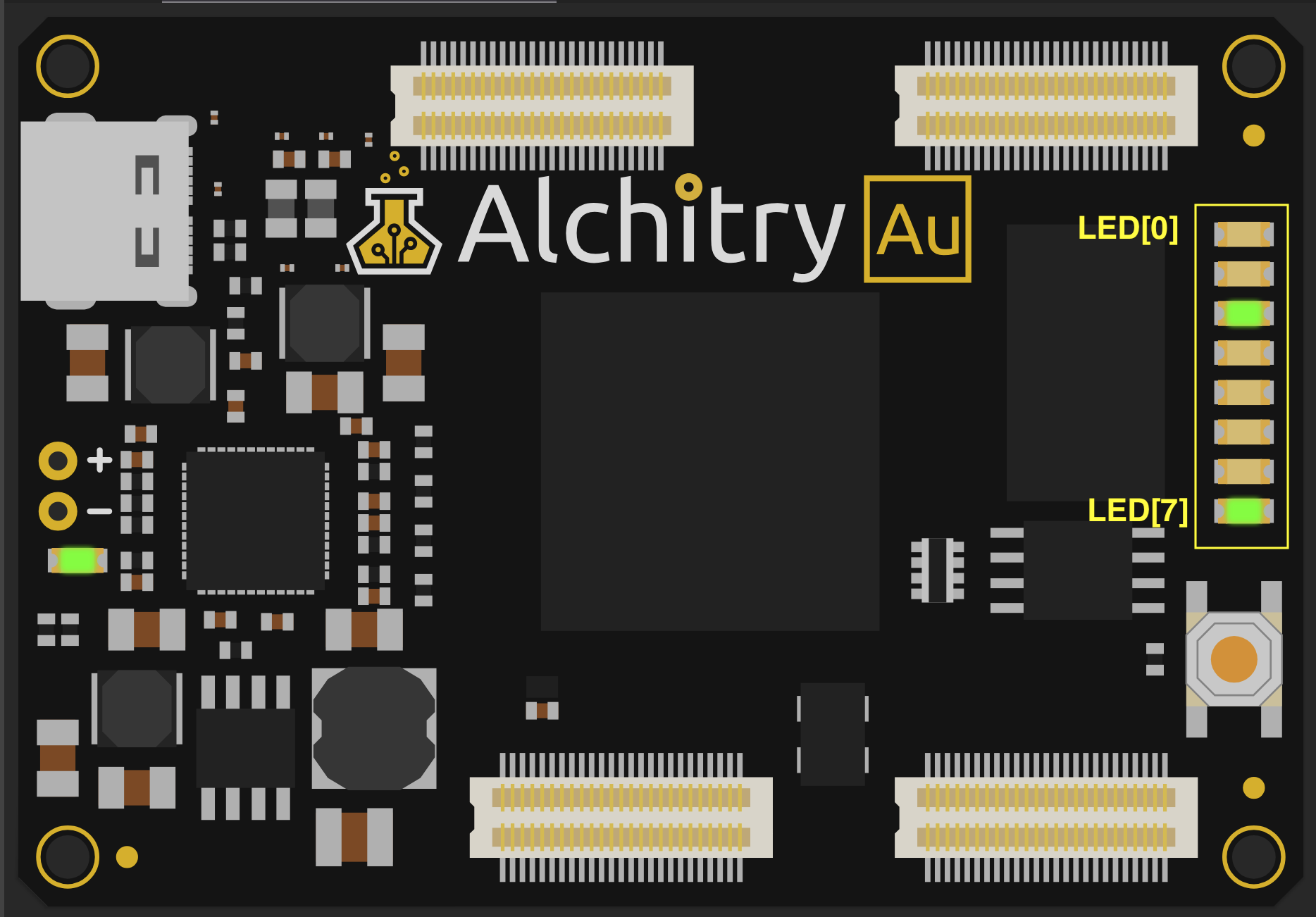
Now click the “bug” (simulation) button and you will see the Alchitry Au interface:

Right now the led does not light up because we set its value into 8h00. This means all 8 bits are 0. Each bit controls one LED from LED[0] to LED[7]. A 0 means off (low voltage), so all LEDs are off.
Change LED value
If we want to light the LED, then we need to set that corresponding LED bit into 1 to light it up, which means “send” high voltage to this led. So for example, if we want the topmost LED to be lit up, we should set its value into:
led = 8b00000001 // each bit is mapped to the LED as an array
You can experiment further with output setting by changing the led setting value inside alchitry_top body into something else, e.g any of the following (choose one):
    led = 8b10000000
    led = 8h80
    led = 10 // decimal 10
    led = 8h84
If you click the simulation button again, you will see that the corresponding LED lights changes. This example uses led = 8h84 assignment.
Note that we didn’t “turn on a light”. We sent a pattern of bits to the FPGA, and each bit controlled one LED. That’s digital logic in its simplest form.
Value assignment
In lucid, when we write the following, we are assigning a value to a signal.
led = 8h00
This is how we tell the FPGA what bit pattern to output.
Every value you assign has two important parts:
- The width: how many bits
- The value: what those bits are
The general format is:
<width><base><value>
Examples:
8b00000001   // 8 bits, binary
8h84         // 8 bits, hexadecimal
8d10         // 8 bits, decimal
If you don’t write a width, Lucid will still try to figure one out but that is risky. Always write the width when controlling hardware.
Understanding the bases
You can write the same number in different bases:
| Syntax | Meaning | Binary form |
|---|---|---|
8b00001010 |
8-bit binary | 00001010 |
8h0A |
8-bit hexadecimal | 00001010 |
8d10 |
8-bit decimal | 00001010 |
All three examples represent the same 8-bit pattern. Only the writing style changes but the FPGA always sees pure binary bits.
Try this in the simulator
Change your line to each of the following and observe what happens in the LEDs:
led = 8b00001010
led = 8h0A
led = 8d10
You should always see the same LEDs turned on, because the bit pattern is the same.
Why width matters
Look at this:
led = 12
This is NOT the same as:
led = 8d12
12 by itself has no fixed width. The tool must guess. What is the problem then?
The Bundle of Wires
In FPGA design, every signal is ultimately just a wire or a bundle of wires carrying bits. When you write led = 8d12, you are not assigning an abstract “number” the way software does. You are sending an 8-bit pattern onto an 8-bit output bus, and each bit drives one physical wire.
Hardware does not stretch or shrink based on the value you write, so you must always choose the correct width.
A bus like led[7:0] is exactly eight wires, no more and no less, and each wire controls one LED. What the FPGA sees is only a pattern of 0s and 1s moving on wires.
So in short, always prefer defining the width of your assignment, for example since you know led is an 8-bit output bus, then write it as so:
led = 8d12
Again, hardware does not “stretch” or “shrink” by magic as each bit is basically the voltage value that is sent via a physical wire.
You must control the number of bits you send.
Multiple Value Settings
Since there is no notion of time or sequence, ALL statements describe hardware that exists at the same time. If the same signal is assigned more than once in the same block, the last assignment takes precedence.
This is not because it “runs later”. It is simply a rule the tool uses to resolve conflicts when multiple lines try to drive the same wire.
For example:
    always {
        ...
        led = 8b00000000
        led[0] = 1
    }
Here led is first set to all zeros, then bit 0 is set to 1. The final result is 00000001. The second line does not “run later in time”. It just overrides the previous assignment for that bit.
This pattern is common: set a default bus value first, then override bits.
Order in an always block is not time. It is priority for conflicting assignments.
Inputs, Interactivity, and Bit-Flow
Now, our goal is to move on from assigning static output into how inputs (via buttons and switches) drive outputs (led values).
You will be given something called the IO-Shield, which is a pre-packaged sets of buttons (5), switches (24), LEDS (24), and 7-segments (which are just LEDs arranged in the shape of numbers).
- It will be stacked on top of the FPGA board and connected to it
- To drive corresponding IO Shield LED or read from the button/switches, we need to have the correct constraint file in our project
Click the “add component” button and select Component Library:

Then expand “Constraints” and select “Io V1 Pulldown”:
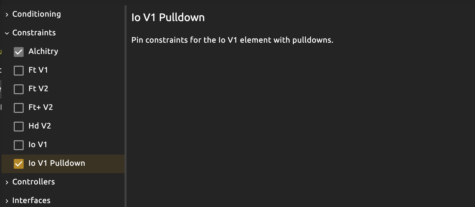
This gives you a new file called io_v1_pulldown.acf that maps pins in the B, A, and C banks into logical names like io_button or io_led.
    // io_v1_pulldown.acf
    PINOUT(V1), STANDARD(LVCMOS33) {
        pin io_led[0][0] B21
        pin io_led[0][1] B20
        pin io_led[0][2] B18
        pin io_led[0][3] B17
        pin io_led[0][4] B15
        pin io_led[0][5] B14
        pin io_led[0][6] B12
        pin io_led[0][7] B11
        pin io_led[1][0] B9
        pin io_led[1][1] B8
        pin io_led[1][2] B6
        pin io_led[1][3] B5
        pin io_led[1][4] B3
        pin io_led[1][5] B2
        ...
    }
Then you need to link these new ports into alchitry_top.luc, which is your main file.
    // alchitry_top.luc

    module alchitry_top (
    input clk,              // 100MHz clock
    input rst_n,            // reset button (active low)
    output led[8],          // 8 user controllable LEDs
    input usb_rx,           // USB->Serial input
    output usb_tx,           // USB->Serial output
    // IO Shield
    input io_button[5],
    input io_dip[3][8],
    output io_select[4],
    output io_segment[8],
    output io_led[3][8]
    )
Output always need a value
When you paste the above, you will be met with error as follows:
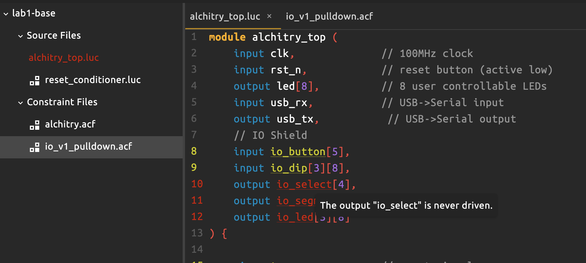
That is because from the tool’s point of view, that output is a wire with no driver, which is illegal/useless hardware.
When you declare output io_select[4], it tells the tool that there are 4 wires leaving this chip. However, since you have yet to assign io_select value anywhere, those 4 wires have nothing connected on the FPGA side.
In HDL, every output must be driven by some logic. If you declare an output but never give it a value, the tool sees a physical pin with no driver, which is a floating, undefined net, so it errors out instead of silently building broken hardware.
To fix this, you can assign some arbitrary value first in the always block:
        io_select = 0
        io_segment = 8hFF
        io_led = 3x{ {8h0} } // this is called an array builder, more on this later
You can change these value later. Now click simulate and you should be able to see the IO Shield now. We label them based on the logical names defined in the constraint files:

Two-dimensional buses:
io_ledis a 3 by 8 bus (24 wires in total)io_dipis also a 3 by 8 bus
To switch on only the rightmost io_led, you can do either of the following:
    io_led[0][0] = 1
    io_led[0] = 8h1
    io_led[0] = 8b00000001
    io_led = {8h0, 8h0, 8h1} // build 3 by 8 array
Consult the Lucid reference guide to learn more about array syntax.
Processing inputs
There are two input sources: button or switches. So far, we only drove led with constants. Now we let inputs (buttons and switches) control the LEDs.
Buttons vs switches
Buttons are usually used as momentary 1-bit inputs (press: 1, release: 0). Switches are stable 1-bit inputs and are convenient to form a multi-bit bus (e.g. 4 switches = 4-bit number).
You can connect input to output port directly to observe its behavior:
    // alchitry_top.luc
    led[4:0] = io_button
    io_led = io_dip
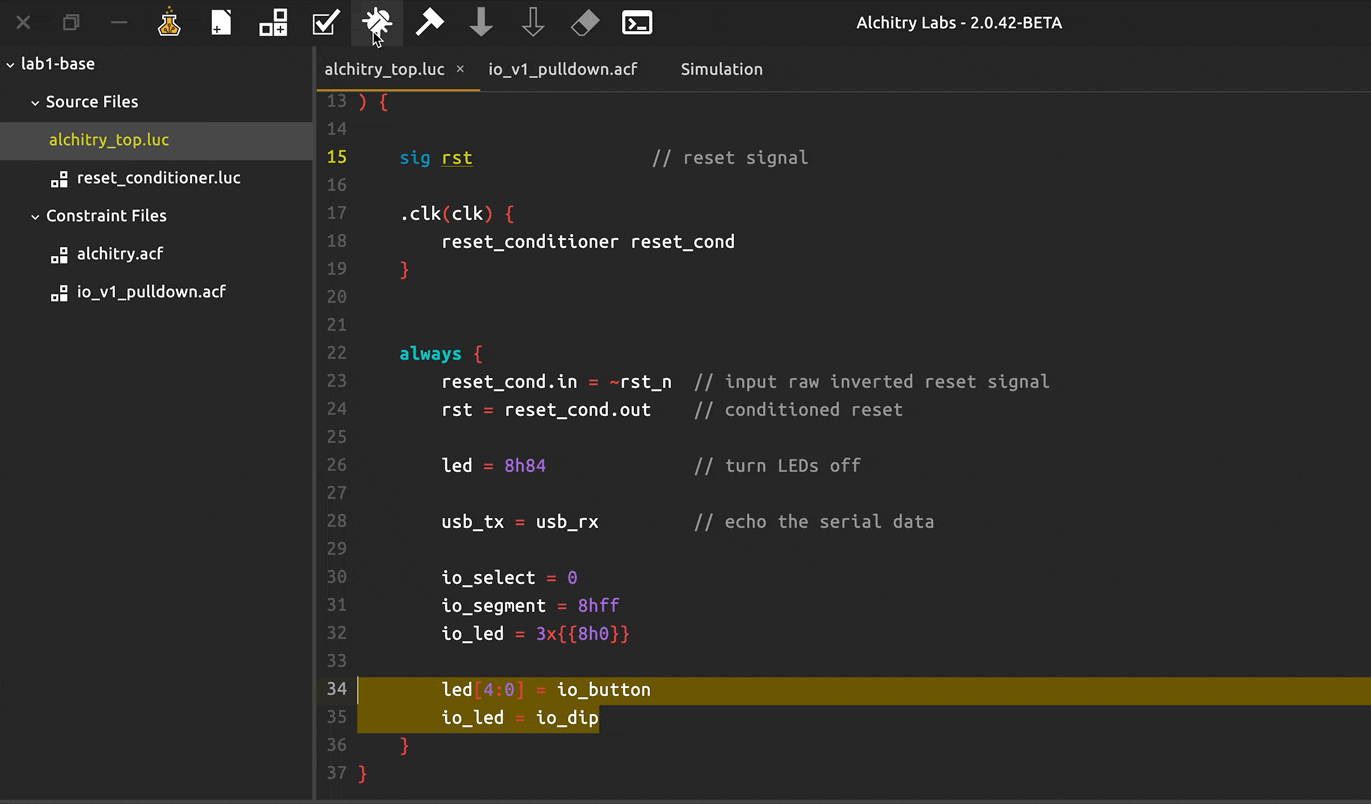
Now we can use the input switches to feed “patterns of information” into the FPGA.
We will not discuss how Seven Segment works in this lab. You can read this guide instead.
Static Discipline in Practice
The static discipline
For valid digital inputs, the circuit must produce valid digital outputs.
This is a well-behaved combinational mapping because every input pattern has a well-defined output pattern:
    always {
        reset_cond.in = ~rst_n  // input raw inverted reset signal
        rst = reset_cond.out    // conditioned reset

        led = 8b00000000             // turn LEDs off

        usb_tx = usb_rx         // echo the serial data

        io_select = 0
        io_segment = 8hff
        io_led = 3x{ {8h0} }

        led[4:0] = io_button
        io_led = io_dip
    }
That is, no matter which button and switch combination is being pressed, we know exactly the state of the LEDs (output bits). There’s no “memory” or state dependence.
Bad Pattern
Now compare with this:
  sig x

    always {
        reset_cond.in = ~rst_n  // input raw inverted reset signal
        rst = reset_cond.out    // conditioned reset

        usb_tx = usb_rx         // echo the serial data

        io_select = 0
        io_segment = 8hff
        io_led = 3x{ {8h0} }

        led[7:1] = 0

        if (io_dip[0][0]){
            x = 1
        }

        led[0] = x


    }
Sig
The
sigtype is short for signal. These are used as basic connections (wiring) between parts of your design. More info about this below.
This is a bad pattern because if io_dip[0][0] is 0, then x will be undefined. Alchitry Labs will detect this (any good HDL editor would) and issue an error:
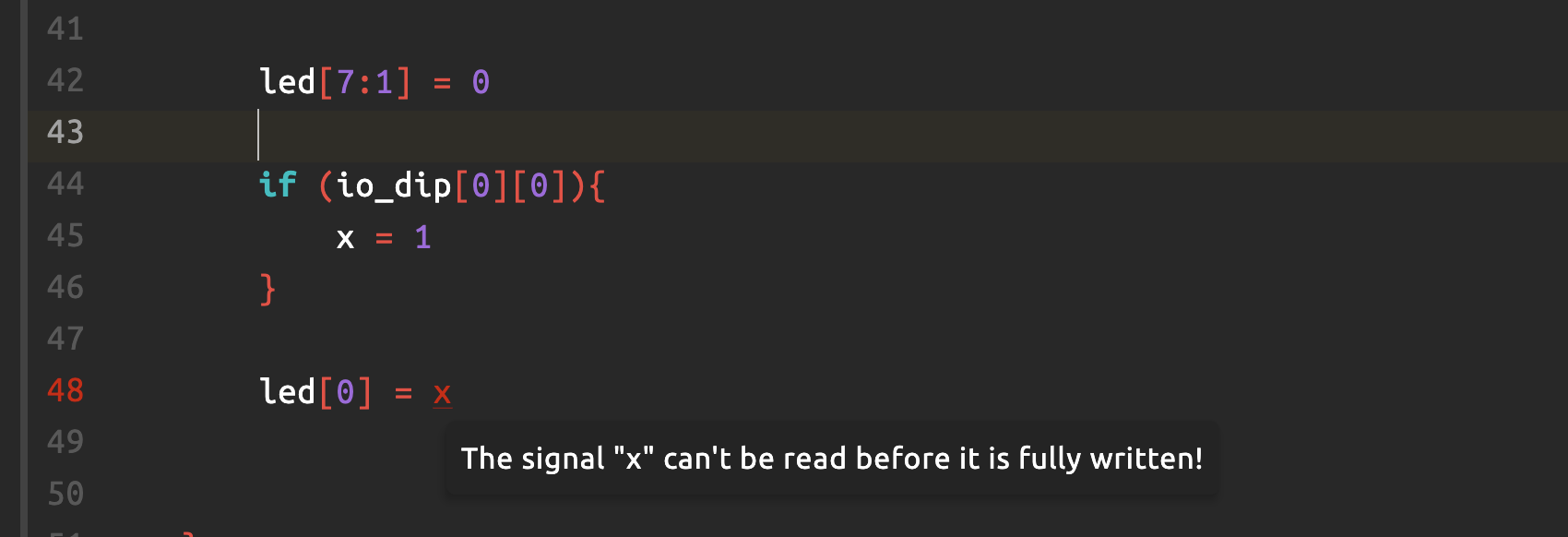
This code breaks static discipline because the output is no longer determined solely by the current inputs. In the later weeks, you will learn about sequential logic, which produces output based on memory. For now, you don’t have to worry about it. We shall cross the bridge when we get there.
Logic Gates (AND / OR / XOR)
In lecture, logic gates are introduced using truth tables.
In HDL, we usually do not build gates explicitly. Instead, we write Boolean expressions, and the synthesis tool maps them to hardware. The logic itself is the same.
Single-bit logic gates in HDL use bitwise operators:
| Gate | Operator | Description |
|---|---|---|
| AND | & |
Output is 1 only if both inputs are 1 |
| OR | | |
Output is 1 if either input is 1 |
| XOR | ^ |
Output is 1 if the inputs are different |
| NOT | ~ |
Inverts a single bit |
You are probably familiar with !, which is a logical NOT (it reduces to 1-bit true/false), and not bitwise. For 1-bit signals, !a and ~a often behave the same, but for “gate thinking”, use ~.
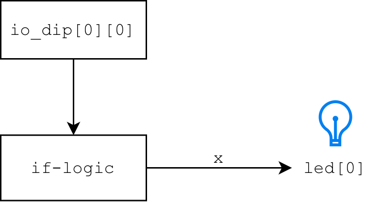
Exploring gates using DIP switches
Use two DIP switches as logic inputs then drive three LEDs using different logic gates like so:
always {
    led[5] = io_dip[0][0] & io_dip[0][1];  // AND
    led[6] = io_dip[0][0] | io_dip[0][1];  // OR
    led[7] = io_dip[0][0] ^ io_dip[0][1];  // XOR
}
Toggle the two switches through all four input combinations and verify the LED outputs matches the truth table.
| a | b | AND | OR | XOR |
|---|---|---|---|---|
| 0 | 0 | 0 | 0 | 0 |
| 0 | 1 | 0 | 1 | 1 |
| 1 | 0 | 0 | 1 | 1 |
| 1 | 1 | 1 | 1 | 0 |
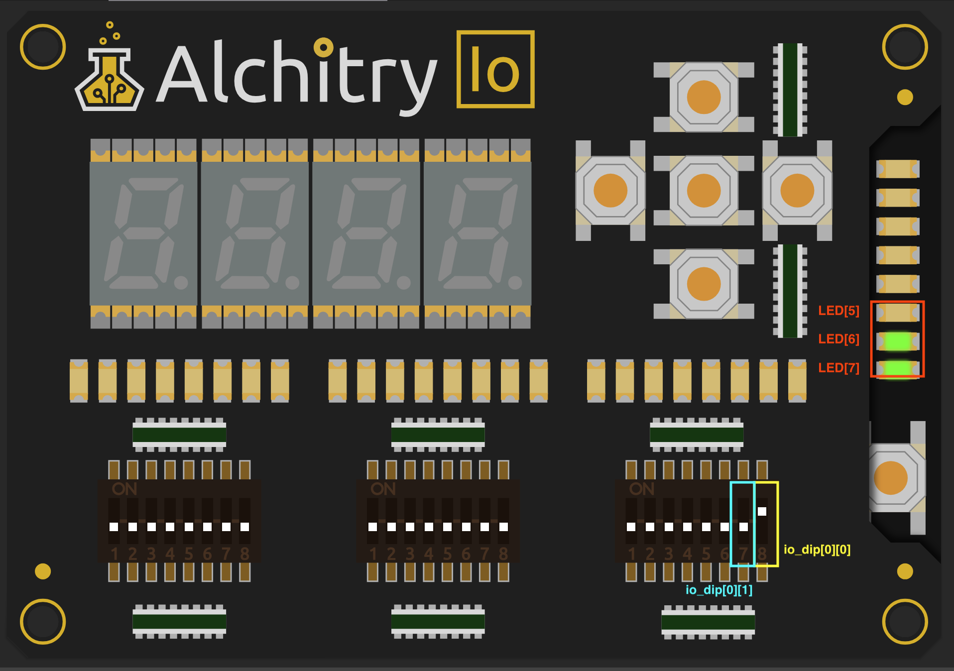
This is the HDL representation of the AND, OR, and XOR logic gates from lecture.
Logic gates are not written as modules
In FPGA designs, we do not create separate AND, OR, or XOR gate modules.
The FPGA fabric already implements logic gates internally. Therefore, writing Boolean expressions is clearer and more efficient. Gate-level modules also do NOT scale and quickly become unreadable.
For example, this is how an AND gate might look as a module:
module and2 (
    input a,
    input b,
    output y
) {
    always {
        y = a & b
    }
}
And you can use it like so:
and2 g_and

always {
    g_and.a = io_dip[0][0]
    g_and.b = io_dip[0][1]
    led[0]  = g_and.y
}
This is functionally correct, but it is awkward and not how real designs are written.
Instead, we shall write the logic directly:
always {
    led[0] = io_dip[0][0] & io_dip[0][1]
}
Both describe the same boolean function.
In later labs, you will build larger modules such as adders, multiplexers, and state machines, not individual logic gates.
Internal sig
So far, we used ports (input / output) to communicate with the outside world. Inside a module, you often need internal wires (like jumper wires used in breadboarding to connect internal components only) to connect pieces together. In Lucid, these are declared using the sig keyword, placed above the always block:
    sig x
    sig y[8]
sig xis 1 wire carrying 1 bitsig y[8]is 8 wires, just like led[8]
A sig is just a named wire (or bundle of wires) inside the module.
Each sig must have exactly one driver, either:
- From logic in an always block, or
- From an output of an instantiated module
If there’s conflicting assignments, the tool will take the latest one (written later in the code).
It is important to understand that sig is NOT equal to variables in regular programming language. sig does not store values. It does not remember anything. It simply carries its current value.
Array Duplication, Builder, and Concatenation
Lucid lets you build bigger buses from smaller parts using {} and the duplication operator Nx{}.
Array Builder
The array builder provides a way to create an array from any number of identically sized expressions.
The syntax is { expr1, expr2, ... } where all expr have the same width.
This builds a 3 by 8 wire bus:
io_led = {8h0, 8h0, 8h0}
Array building like the above is the same as writing:
    io_led[0] = 8h0
    io_led[1] = 8h0
    io_led[2] = 8h0
Duplication
Instead of writing the same thing many times, you can use duplication:
io_led = 3x{ {8h0} } // repeat 8h0 3 times, to fill the whole 3×8 array.
Duplication is useful when working with large arrays that require repetition such as driving LED matrices.
There’s no right and wrong way to build an array. Sometimes, the simplest method is best, that is io_led = {8h0, 8h0, 8h0}. You don’t need to over-refactor or over-engineer your HDL code, and certainly there’s no need to apply your “clean code” software principles here, unless you’re already experienced in HDL. Remember that this is a group work and group members have various background. So let’s stick with the “simple is best” philosophy for now.
Concatenation
If you want to merge two or more buses with differing width, you can use concatenation. Concatenation provides a way to merge two or more arrays.
It takes the form c{ expr1, expr2, ... } where all expr are arrays or bits.
If the values passed into it are multi-dimensional arrays, all of their sub-dimensions must match. For example, an array of width [2][8] could be concatenated with an array of width [3][8] to form an array of width [5][8].
Auto Truncation, Auto Extension, and Width Mismatches
In an ideal, strictly-typed world, every signal assignment would have perfectly matching widths. In reality, Lucid is permissive and will try to “help” you by automatically resizing values when the widths do not match. This makes code compile, but it can also silently change the meaning of your circuit. You should consult the documentation to find out more.
In life, you should treat any width mismatch as a design error, even if your IDE allows it.
Auto extension (narrow to wide)
When the right-hand side is narrower than the left-hand side, Lucid will EXTEND the value to fit the target width by adding 0s to the most significant bits.
// io_led[0] is 8 bits
io_led[0] = hF      // hF is 4 bits: 1111
Lucid interprets this as:
0000 1111 -> 8b00001111
No new “value” was created. Four new wires were simply tied to 0 to make the widths match. This is convenient, but dangerous if you are not tracking the widths mentally (see next Lab’s pitfalls).
Auto truncation (wide to narrow)
When the right-hand side is wider than the left-hand side, Lucid will truncate the value by discarding the most significant bits.
// io_led[0] is 8 bits
io_led[0] = 16h00FF
Binary form of the right-hand side:
0000 0000 1111 1111 (16 bits)
After truncation:
1111 1111 → 8b11111111
The top 8 bits are simply thrown away. Those wires never connect to anything. Again, Lucid will compile this, but you must be consciously aware that half the information is being destroyed.
Dimension mismatch (2D vs 1D)
Automatic fixing does not apply to dimension mismatches.
// io_dip is a 3×8 array (3 rows of 8 bits)
io_led[0] = io_dip    // INVALID
Here the problem is not just width but structure. You are trying to connect a 2-dimensional bus into a 1-dimensional bus. Alchitry Labs V2 will show an error with this.
Instead, you must explicitly select one row:
io_led[0] = io_dip[0]
The understanding that must NOT change
Even though Lucid may auto-truncate or auto-extend for you, the physical reality (once you compile and build for the FPGA) is still this:
- Every signal is a fixed number of wires
- Every assignment is connecting specific wires to specific wires
- Bits do not appear or disappear “magically”
- Extra bits are either discarded or tied to 0
You should always be able to answer this before trusting an assignment:
Exactly which bits end up on which physical wires?
If you cannot answer that, your design is already broken, even if the simulator shows something “working”.
Other HDLs
In Verilog (and by extension SystemVerilog) you can assign signals of mismatched widths, and the language defines rules for how the extra bits are handled.
- If the right-hand side (RHS) has more bits than the left-hand side (LHS), the extra most-significant bits are discarded (truncated).
- If the RHS has fewer bits than the LHS, the assignment is zero-extended (for unsigned context) into the extra high bits.
- Because of this implicit behavior, width mismatches often do not cause synthesis errors but they can cause unintended behavior.
- Good style and many lint tools flag width mismatches because they are a common source of bugs.
You should treat mismatched-width assignments in Verilog as dangerous even though the language allows them. Even though Verilog/Lucid allows auto truncation/extension, WE must act as if it does not, and always explicitly match widths or slice/concatenate.
Digging Deeper into the Always Block
These examples all use the same pattern and are created to serve as examples to remind you that everything inside is continuous hardware, not a step-by-step program.
always {
    // connections and logic here
}
1. Simple pass-through
always {
    io_led[0] = io_dip[0]   // copy 8-bit row 0 of switches to row 0 of LEDs
}
Whatever pattern you set on io_dip[0] appears on io_led[0]. Same inputs always leads same outputs. No memory involved and this is what we call a pure combinational logic.
2. Default then override (last assignment wins)
always {
    io_led[0] = 8b00000000  // default: all off
    io_led[0][0] = 1        // override bit 0
}
Final result we will see is that the rightmost io led in the rightmost group of the IO Shield will turn on as we set its bus value to be: io_led[0] = 8b00000001.
There is no concept of time here. The second assignment simply overrides bit 0 of the first assignment, since that’s how priority of conflict is resolved by the tool (Vivado).
3. Good if / else (no memory)
sig x

always {
    if (io_button[0]) {
        x = 1
    } else {
        x = 0
    }

    io_led[0][0] = x
}
The value for x is assigned in both branches.
- For every valid input of
io_button[0],xand the LED are fully defined. - This is good static discipline: output depends only on the current input.
4. Bad if (incomplete assignment, wants memory)
sig x

always {
    if (io_button[0]) {
        x = 1
    }
    io_led[0][0] = x
}
- When
io_button[0] = 1,xbecomes 1. - When
io_button[0] = 0,xis never assigned in this cycle.
To make this work, our design would need to “remember” the old x, which means state. We can do this by building a latch (sequential logic). We will do this in the later weeks.
This breaks the clean static discipline idea as the LED (output) no longer depends only on current inputs.
5. Multiple independent outputs in one always
always {
    // row 0 LEDs show switches
    io_led[0] = io_dip[0]

    // LED[5], LED[6], LED[7] show AND / OR / XOR of two bits
    led[5] = io_dip[0][0] & io_dip[0][1]
    led[6] = io_dip[0][0] | io_dip[0][1]
    led[7] = io_dip[0][0] ^ io_dip[0][1]
}
All these assignments are in effect at the same time.
- There is no “first do io_led, then compute AND, then compute OR.”
- The hardware is just a bunch of parallel wires and gates.
A Caveat: Evaluation Order
always describes parallel hardware, but Lucid/Verilog/other HDL compilers resolves assignments in order.
A common confusion is thinking that if you write out = x and later you change x, then out should automatically “follow” the new x. That would be true if x were a normal programming variable (like a pointer).
In Lucid/HDL, sig or equivalent is NOT a stored variable, it is a named wire driven by logic, and an always block is not a sequence of runtime steps. The FPGA hardware is always parallel. However, the compiler still has to decide what each signal is connected to, and it does that by processing the always block from top to bottom, using the pattern “set defaults first, then override later.”
Consider this tricky example:
module foo (
    input clk,
    input rst,
    input  a,
    output out,
    output cval
) {
    sig x

    counter c(.clk(clk), .rst(rst))

    always {
        x = a
        out = x

        x = c.value
        cval = c.value
    }
}
Would out be the same as c.value since they both refer to x?
After synthesis, there is no notion of “line 1 runs, then line 2 runs” and everything becomes fixed connections.
The key is that the line out = x connects out to whatever x means AT THAT POINT in the always block. At that moment, the most recent definition of x is x = a, so out becomes connected to a.
When the compiler later sees x = c.value, it updates the driver of x (the wire x now comes from c.value), but it does not go back in time and rewrite the already-constructed connection for out.
So the final hardware connections are effectively:
out  = a
x    = c.value
cval = c.value
This is why it is best practice to write always blocks in a “defaults then overrides” style. If you want out to use the counter value, you must place that assignment before out = x, or just drive out directly:
always {
    x = c.value
    out = x
    cval = c.value
}
It is important to understand that** the hardware is parallel**, but the always block is an ordered description that the compiler uses to construct those parallel connections.
Summary
We would like to remind you that in this lab, we did not “write a program” but instead, we described hardware using HDL.
In HDL, we are not just “assigning a number”. We are assigning a bit pattern to a bundle of wires. Each bit travels down one wire. Each wire controls one LED. That is digital hardware.
We have learned quite a few things:
- A signal is a wire. A bus is a bundle of wires.
- Every assignment is a bit pattern, not just a number.
- An
alwaysblock is not sequential code. It represents continuous, parallel hardware. - Each output must be driven, or the design is invalid.
- Each
sigmust have exactly one driver. - Order in an
alwaysblock is not time. It is conflict resolution. - Valid inputs must always produce valid outputs: this is static discipline.
- Missing assignments create undefined values and imply memory, which you are not allowed to use yet.
In the next lab, we will use the same ideas to build a multi-bit combinational system: a ripple-carry adder, multiplexers, and decoders.
Head to eDimension to complete questionnaires (2%) related to this lab.