 50.002 CS
- Overview
- Vivado Starter Project
- Create a New Vivado Project (From Scratch)
- Creating Design Sources in Verilog
- Reset and Button Conditioners
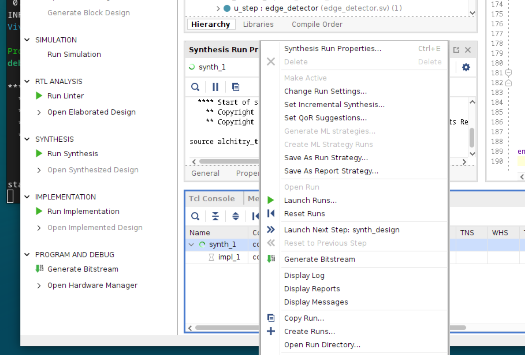
- Reset Runs
- Viewing LUTs Usage
- Timing Summary
Using Vivado + Verilog with Alchitry Au
This guide is written for students who want to entirely skip using Alchitry Labs V2 and code their RTL in Verilog using Vivado (or other tools). You can use Verilog simulator like Icarus-Verilog to test and verify your code, and then turn to Vivado to compile the output.
Using Vivado is out of the syllabus, and we will not be giving you any tutorial on how to use it. This guide is meant to give you enough starter code (constraints and top module) and steps to generate a binary to be loaded to your Alchitry Au board.
Overview
Vivado (from AMD/Xilinx) is a full FPGA toolchain. It can do the following tasks:
- Elaborate/simulate (with its own simulator, optional),
- Synthesize RTL into gates for a specific FPGA,
- Place and route,
- Generate outputs like .bit (bitstream) and optionally .bin, plus timing/utilization reports.
It is vendor-specific (Xilinx/AMD devices). When you clicked the build button, Alchitry Labs V2 IDE calls Vivado via CLI to generate the bitstream for you.
Icarus Verilog (iverilog) is mainly an RTL simulator/compiler. Many people use this instead of Vivado to:
- Compile and run Verilog testbenches, produce VCD waveforms.
- It does not synthesize for an FPGA and does not generate bitstreams.
It is great for fast unit tests and planning.
Here’s a recommended workflow:
- Write RTL + testbench in your code editor of choice.
- Run iverilog for quick correctness checks.
- Use Vivado when you need synthesis, timing, and the bitstream for your FPGA and import the files you created in the previous steps
Vivado Starter Project
Vivado 2025.2
The starter project is created using Vivado 2025.2. If you do not use this version, you can create one from scratch by reading this section.
Clone this repository to obtain the starter code.
This contains the same code that implements the IO V1 Demo Pulldown project that you can create using Alchitry Labs, to run on Alchitry Au FPGA:
Open the Project
Opening the project should give you this window.
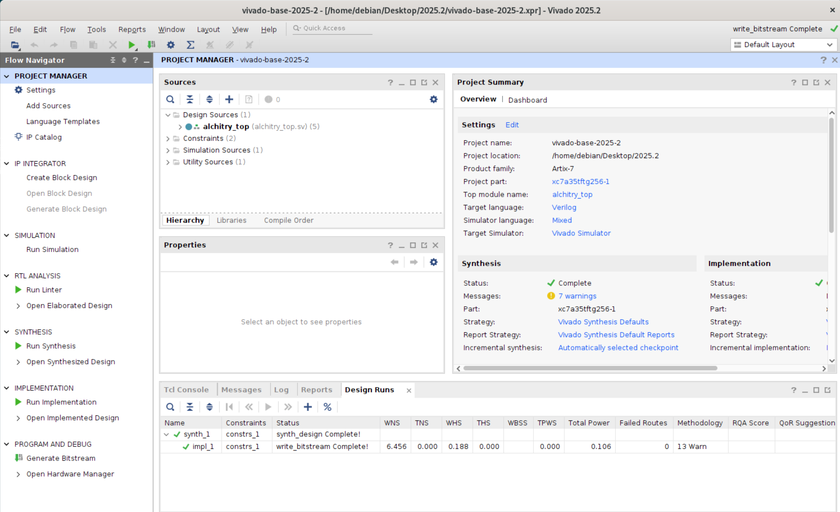
You can try to Generate Bitstream (bottom left of the window) to compile the sources. After synthesis and implementation is completed, you should find the binary alchitry.bin under the directory <PROJECT_DIR>/<PROJECT_NAME>.runs/impl_1/alchitry_top.bin:
Alchitry Loader
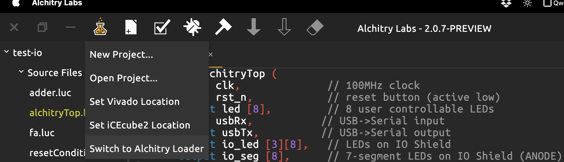
Use Alchitry Loader to load the .bin file to the FPGA.
First, you need to have Alchitry Labs installed. Download Alchitry Lab 2 from here.
Then switch to Alchitry Loader first:
Find the synthesized binary and load it to your Alchitry Au FPGA:
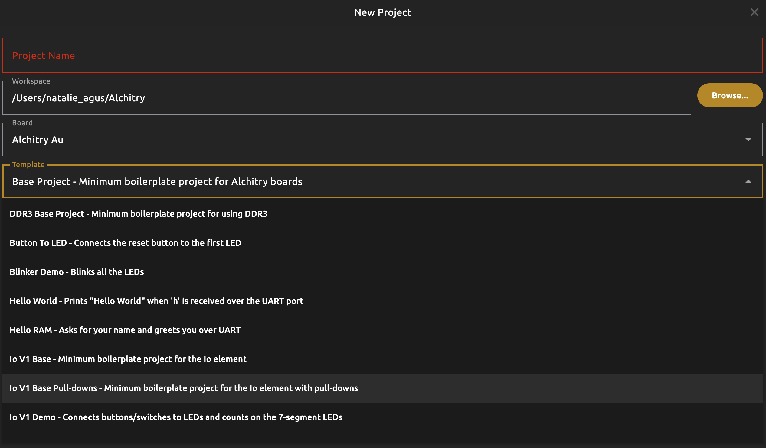
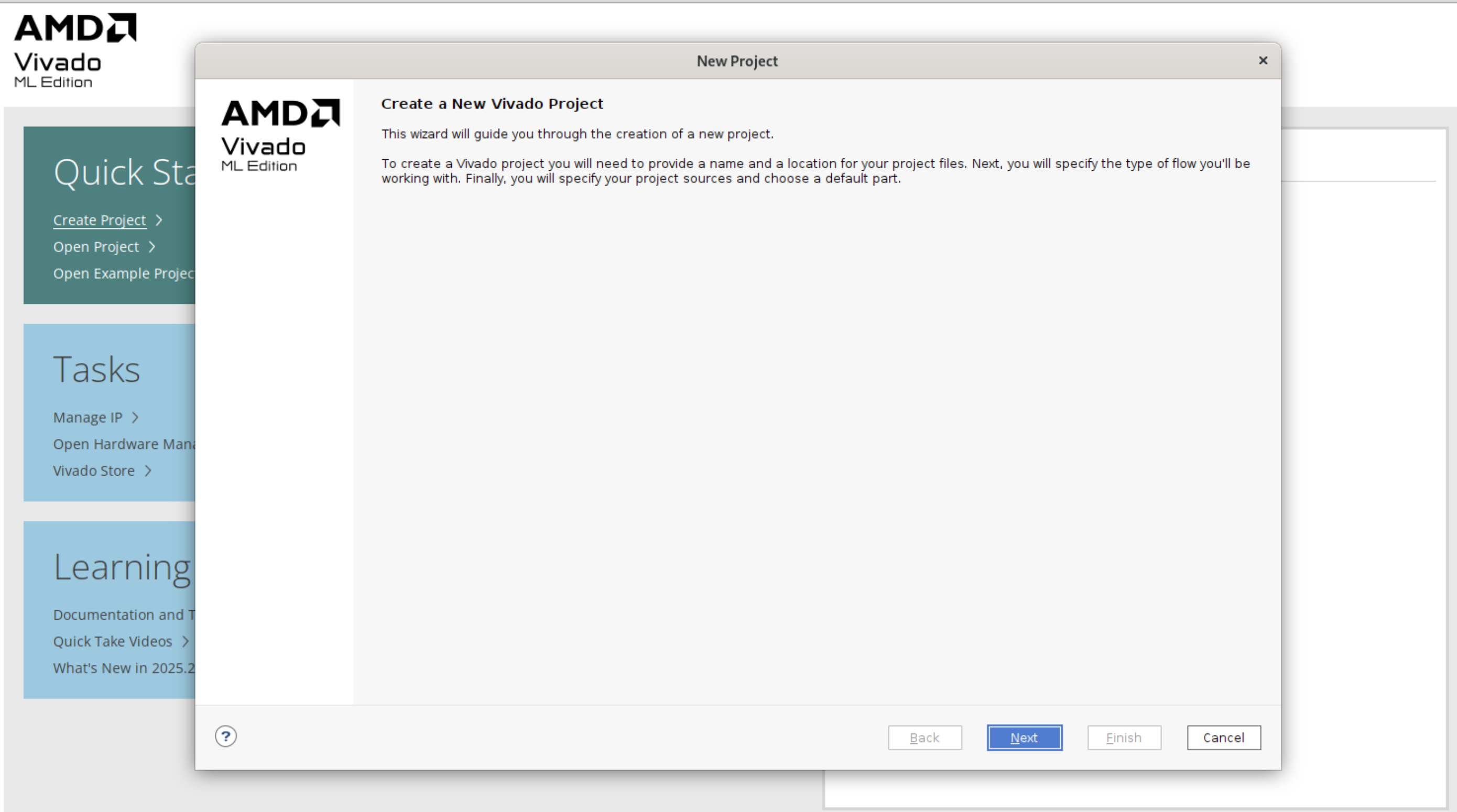
Create a New Vivado Project (From Scratch)
This section is written to help you set up a new Vivado project if you can’t open the starter project given because of version differences (you did not use 2025.2).
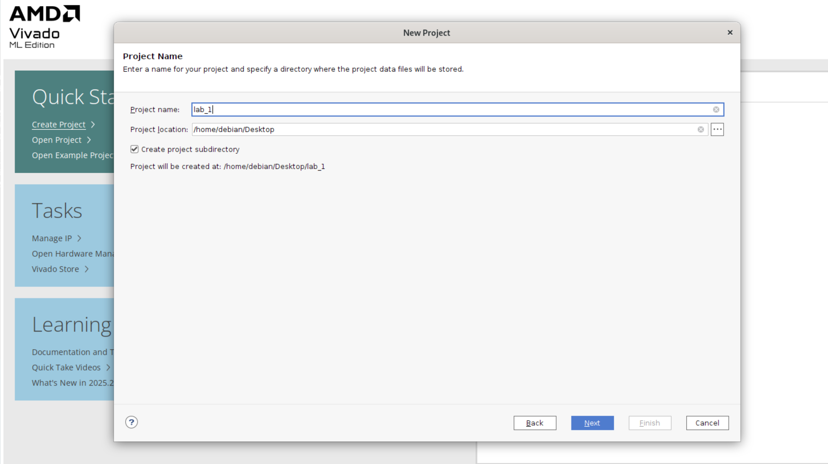
First, create a new project:
Click next, decide the project path:
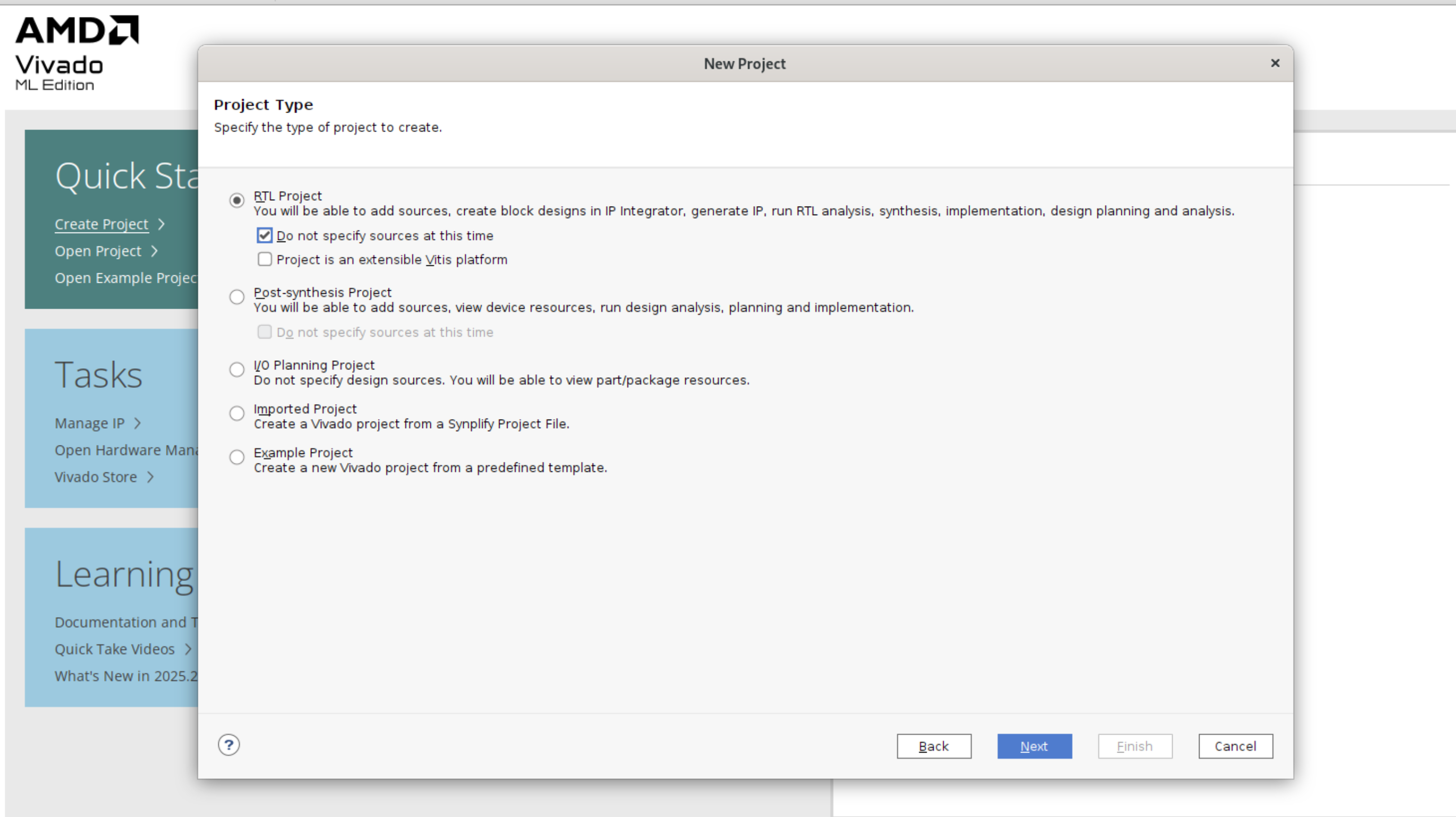
Select RTL project, click “do not specify sources at this time”:
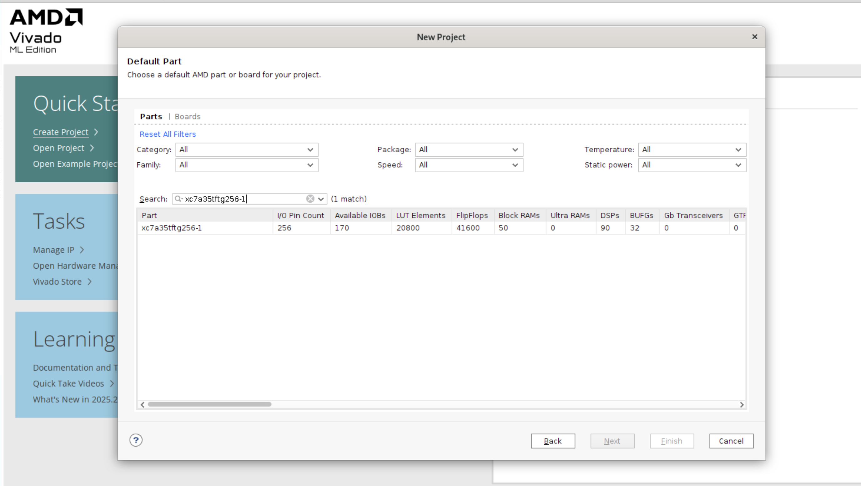
Select the parts: xc7a35tftg256-1. This is our Artix-7 FPGA inside Alchitry Au:
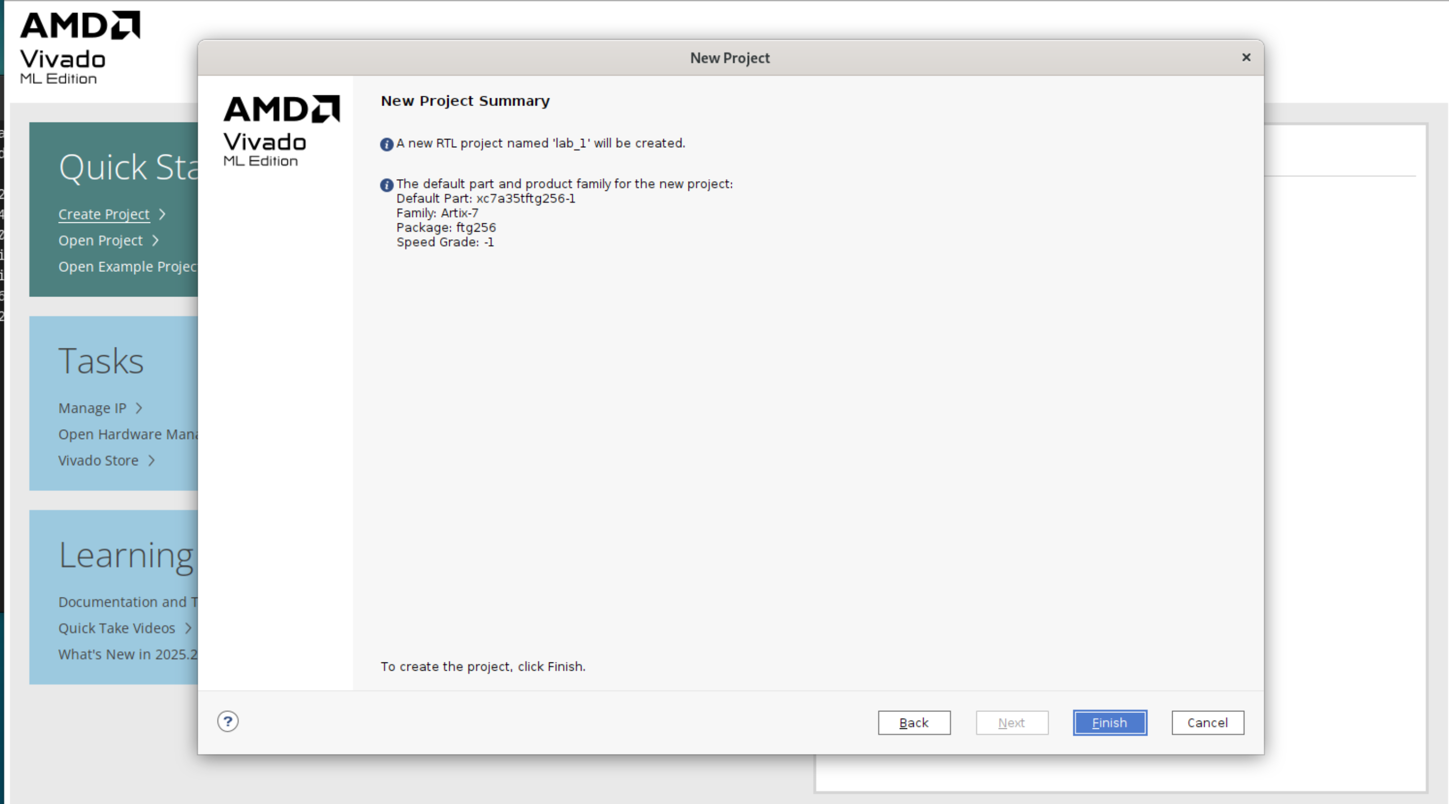
View the summary page then click Finish:
You will now see this window:
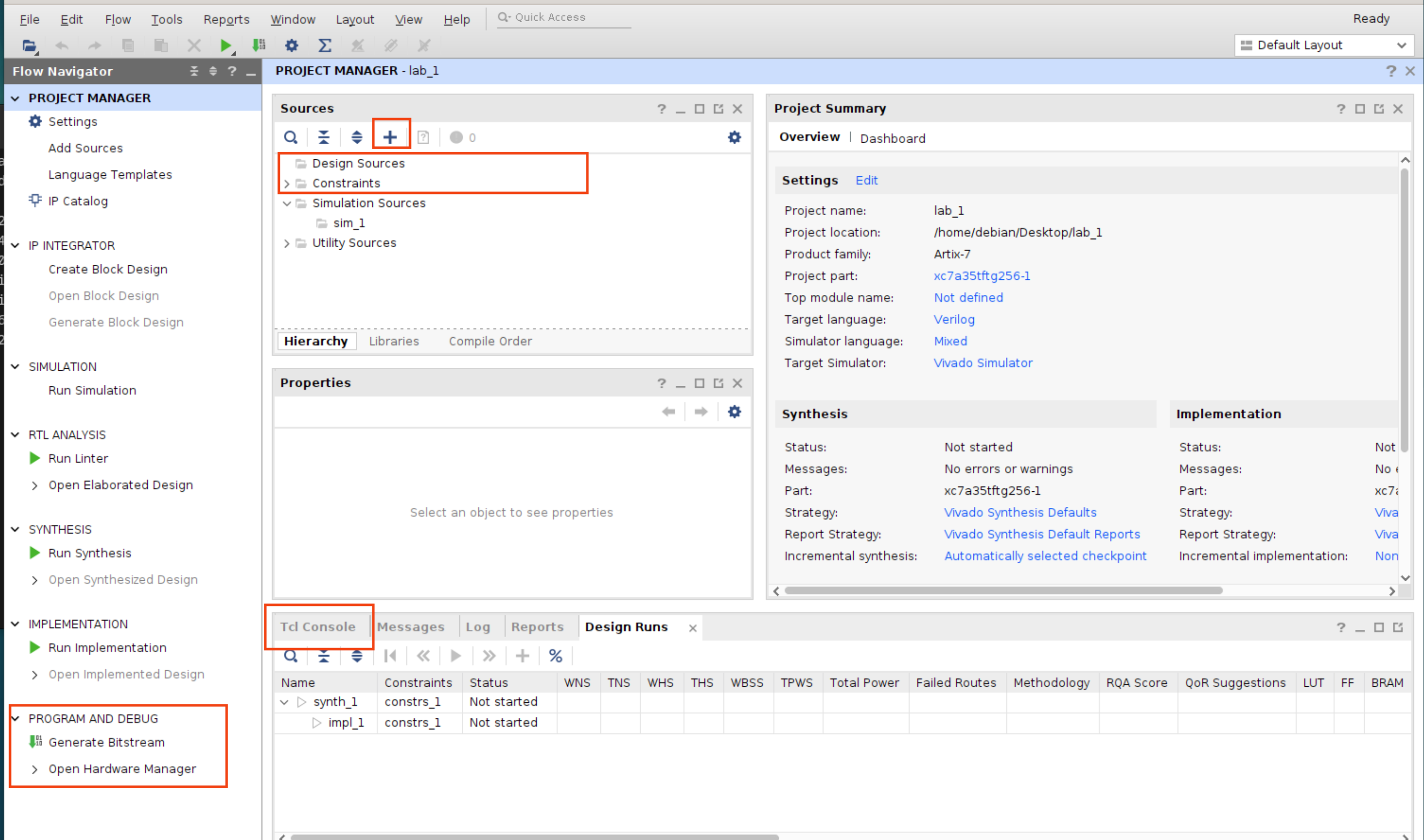
Pay attention to the sections highlighted in the screenshot above.
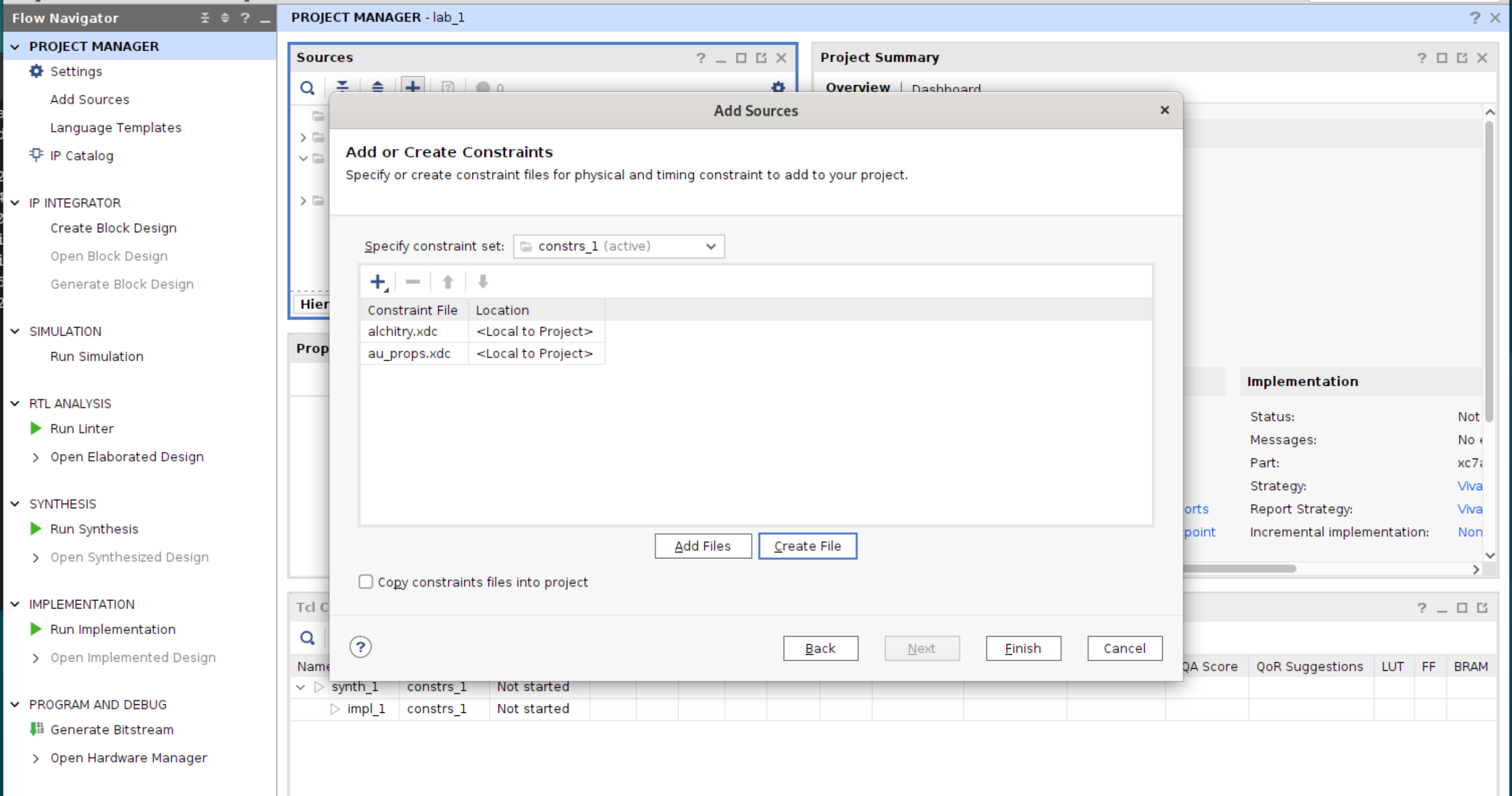
Create Constraint Files
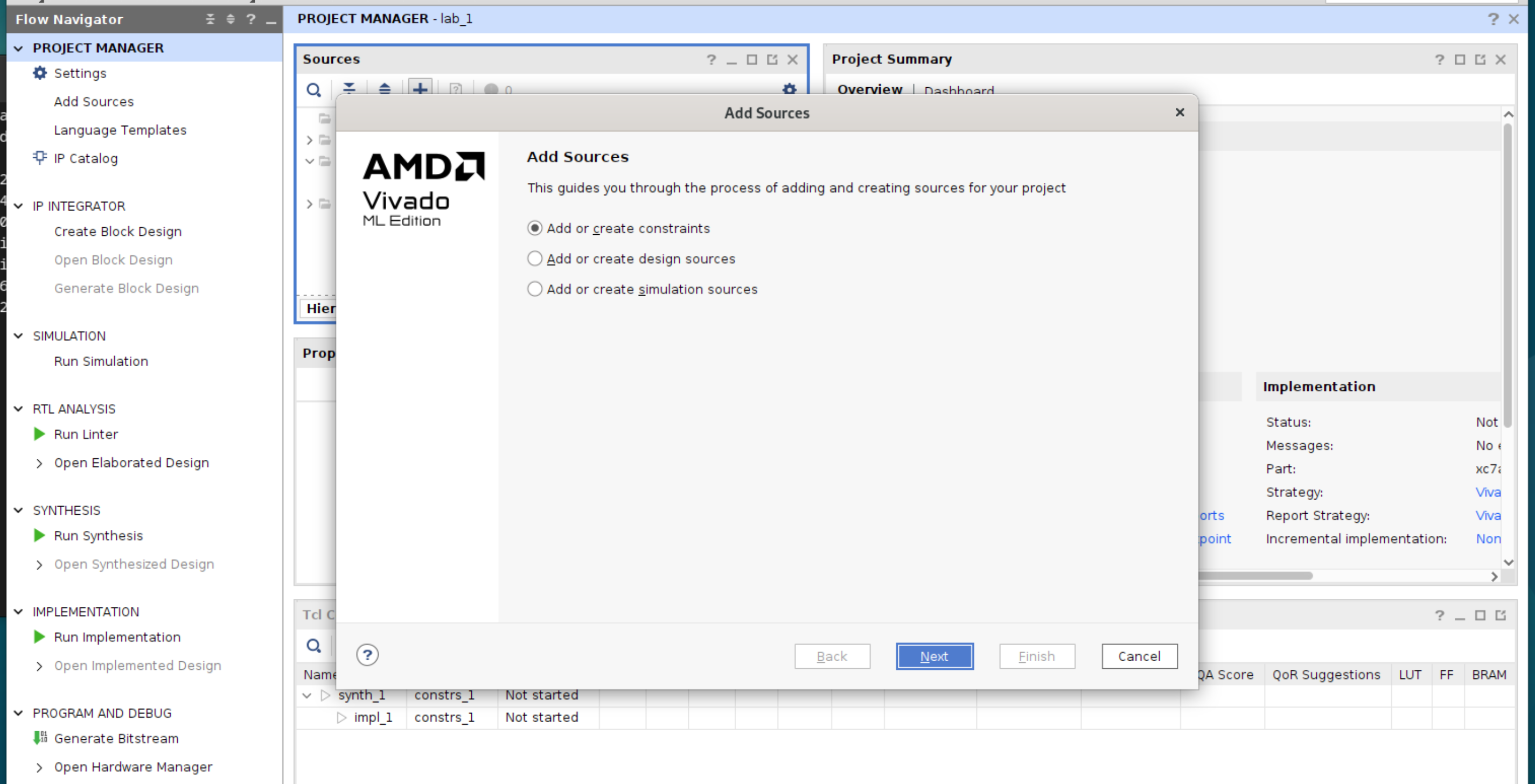
Click the + button under Sources pane, and select Add or create constraints:
Then click Create File. Create 2 new files: alchitry.xdc and au_props.xdc. When done, click finish.
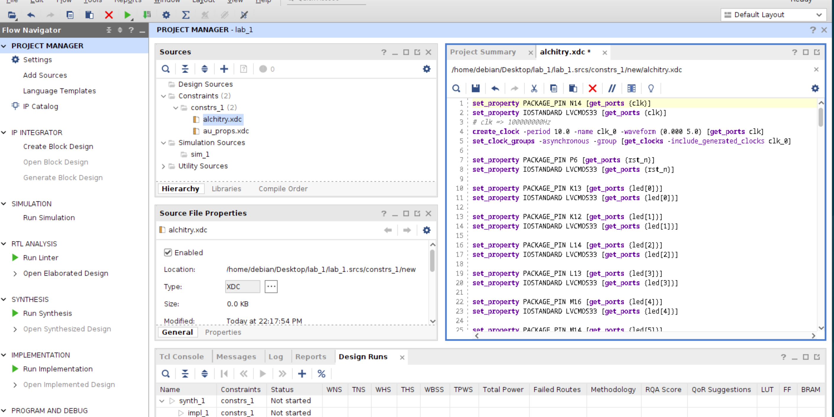
Then open alchitry.xdc from the Sources pane, and paste this content into it, and save it:
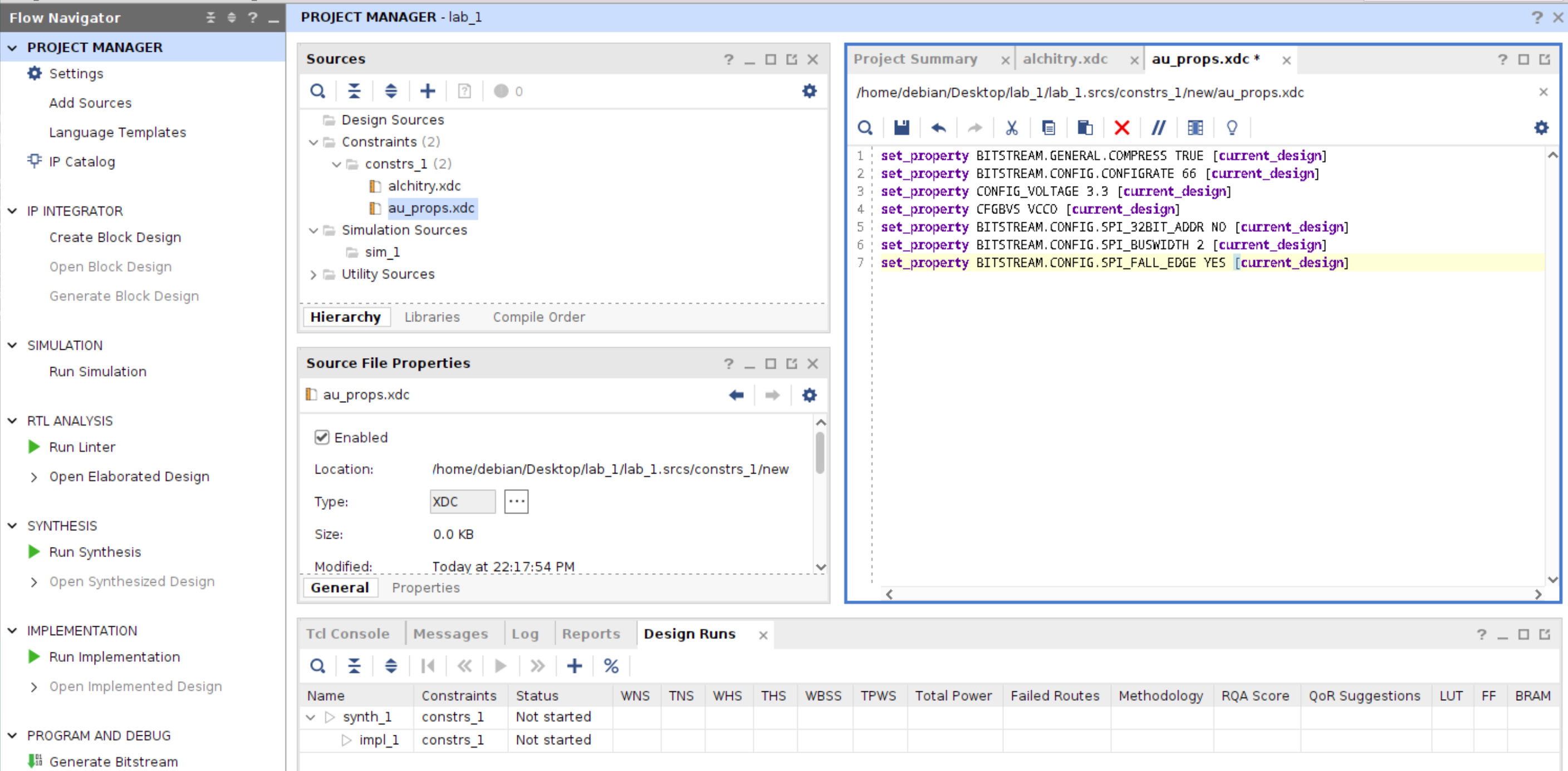
Afterwards, open au_props.xdc and paste this content into it:
About Constraints
In a Vivado project, the constraint file (XDC) is where you tell Vivado everything your RTL does not say:
- How your top-level ports connect to the real FPGA package pins (pinout)
- What electrical standard each pin uses (voltage, IO standard, pulls, drive, slew, etc.)
- Timing intent (what clock frequency you’re targeting, which clocks are unrelated, false paths, etc.)
- Bitstream and configuration options (how the FPGA will be programmed, SPI width, config rate, compression)
If you don’t constrain these, Vivado will guess or leave defaults, and you get stuff like: wrong pins, wrong voltage standard, floating inputs, or timing that “passes” in a meaningless way.
Each of the section below explains the high-level understanding behind the lines you pasted into au.xdc and alchitry.xdc.
Bitstream / configuration (how programming behaves)
These affect how the .bit (and possibly .bin) is generated and how the FPGA config logic talks to the flash/programmer.
set_property BITSTREAM.GENERAL.COMPRESS TRUE [current_design]
Compress the bitstream. Smaller file, faster to transfer sometimes. Slightly more decompression work during config (usually fine).
set_property BITSTREAM.CONFIG.CONFIGRATE 66 [current_design]
Requested configuration clock rate (in MHz) used during configuration. Too aggressive can make config unreliable on some boards; board design matters.
set_property CONFIG_VOLTAGE 3.3 [current_design]
set_property CFGBVS VCCO [current_design]
These describe the configuration bank voltage environment. In plain terms: “assume config related IO is at 3.3 V, and the config bank voltage source is VCCO”. Helps ensure the bitstream/settings are consistent with the board’s voltage scheme.
set_property BITSTREAM.CONFIG.SPI_32BIT_ADDR NO [current_design]
set_property BITSTREAM.CONFIG.SPI_BUSWIDTH 2 [current_design]
set_property BITSTREAM.CONFIG.SPI_FALL_EDGE YES [current_design]
SPI flash configuration behavior:
SPI_BUSWIDTH 2: use dual-SPI (2 data lines) during configuration.SPI_FALL_EDGE YES: sample on falling edge (board/flash timing requirement).SPI_32BIT_ADDR NO: use 24-bit addressing mode (relevant for larger flashes and how commands are emitted).
Physical pin mapping + electrical standard (makes signals land on the right wires)
This is the “your Verilog port named clk is physically on pin N14 and is a 3.3 V CMOS IO” part.
set_property PACKAGE_PIN N14 [get_ports {clk}]
set_property IOSTANDARD LVCMOS33 [get_ports {clk}]
PACKAGE_PIN N14ties yourclkport to the FPGA package ball/pin N14 (board-specific).IOSTANDARD LVCMOS33says it’s a 3.3 V single-ended CMOS IO standard.
Same idea for rst_n, led[0], usb_rx, etc.
Timing constraints
create_clock -period 10.0 -name clk_0 -waveform {0.000 5.0} [get_ports clk]
Declares clk as a 100 MHz clock:
- period 10 ns
- waveform rising at 0, falling at 5 ns (50% duty)
This is used by timing analysis, so that you can get a design that “builds” and does not fail on hardware.
Input conditioning (avoid floating inputs)
These matter a lot for switches/buttons because they can float and randomly toggle.
Example:
set_property PULLDOWN true [get_ports {io_button[0]}]
Enables an internal pulldown resistor on that FPGA input, so the signal defaults to 0 when the button/switch is open (assuming the board wiring matches that expectation). We set pulldowns on DIP and buttons, which is typical.
Create Design Sources
This is where your verilog files live. Create a new design source called alchitry_top.sv (System Verilog). This is your top module.
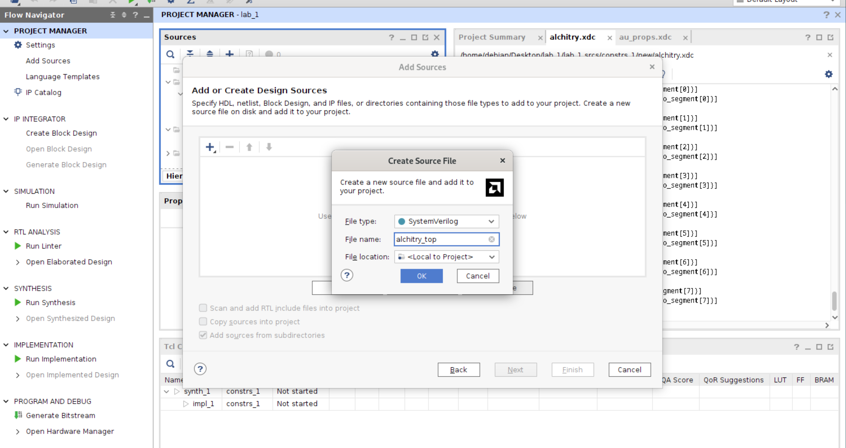
You can use Verilog for your other modules, but for the top modules, we use SystemVerilog to support the 2D array io_led and io_dip defined in the constraint file. You can flatten it later in the later modules.
You can define the ports now, or later in the script. In this example, we define just the clk port from the GUI:
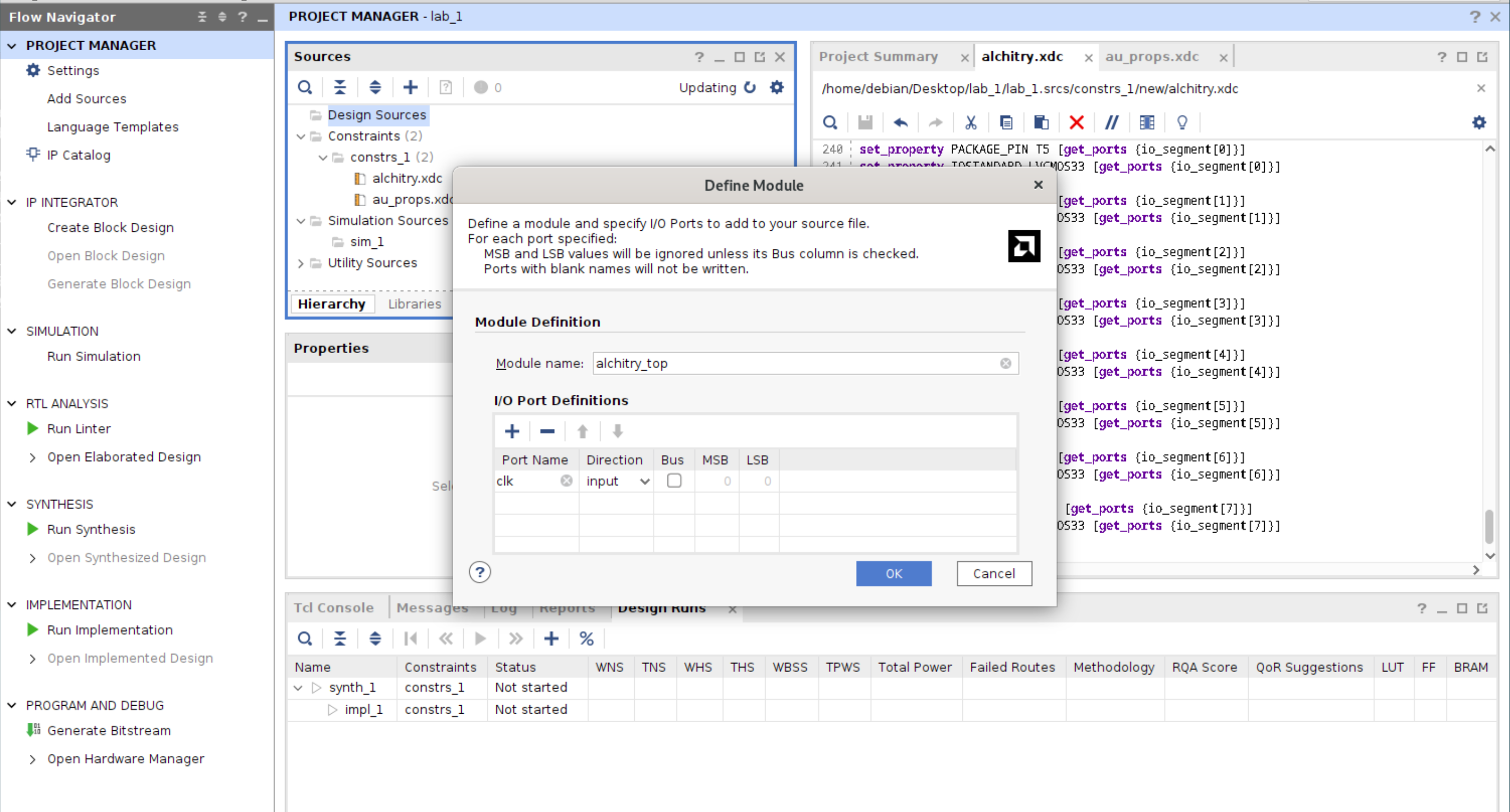
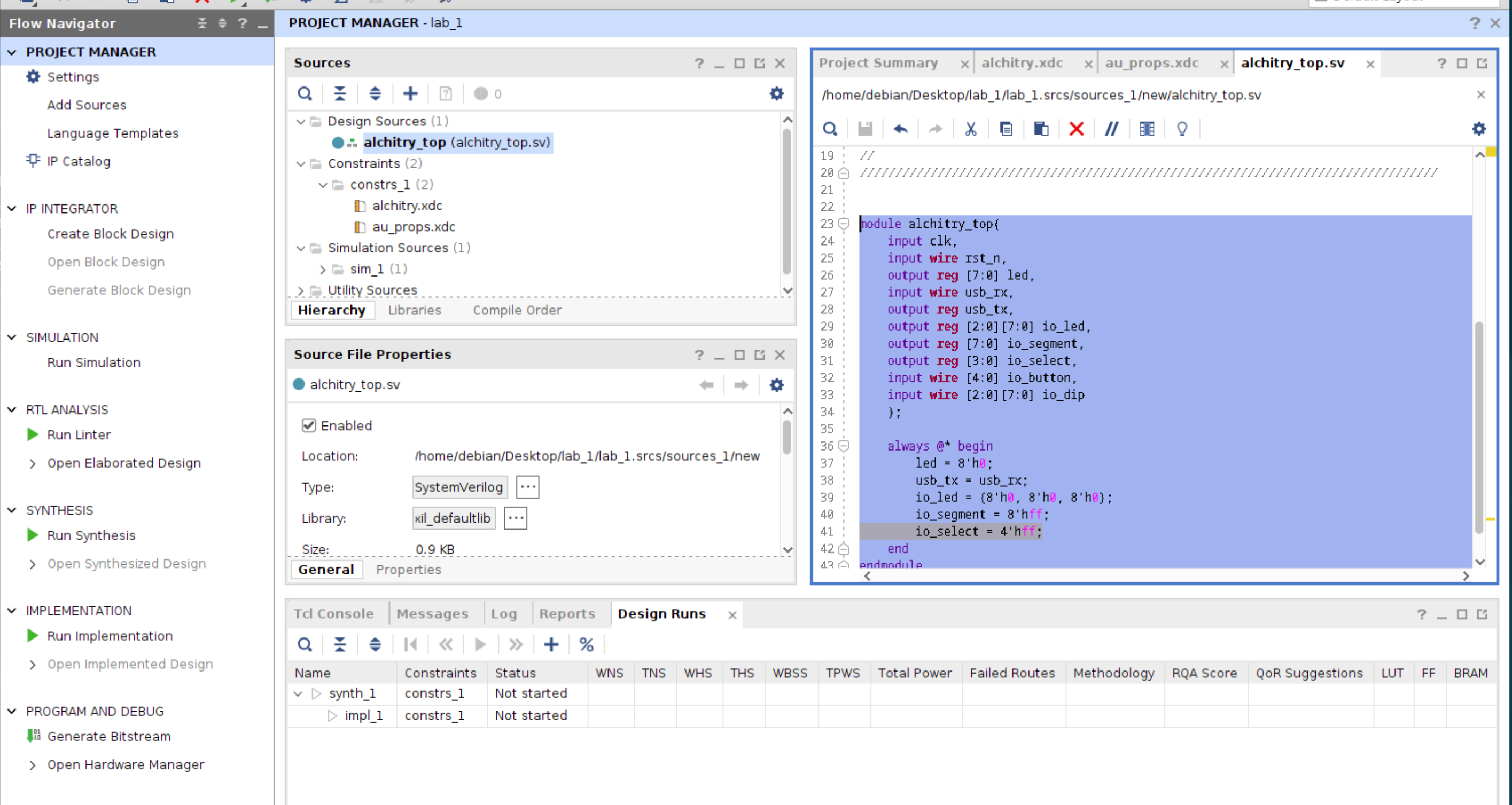
Once you have the following alchitry_top.sv file, add the remaining ports, as well as the default connections:
module alchitry_top(
    input clk,
    input wire rst_n,
    output reg [7:0] led,
    input wire usb_rx,
    output reg usb_tx,
    output reg [2:0][7:0] io_led,
    output reg [7:0] io_segment,
    output reg [3:0] io_select,
    input wire [4:0] io_button,
    input wire [2:0][7:0] io_dip
    );

    always @* begin
        led = 8'h0;
        usb_tx = usb_rx;
        io_led = {8'h0, 8'h0, 8'h0};
        io_segment = 8'hff;
        io_select = 4'hff;
    end
endmodule
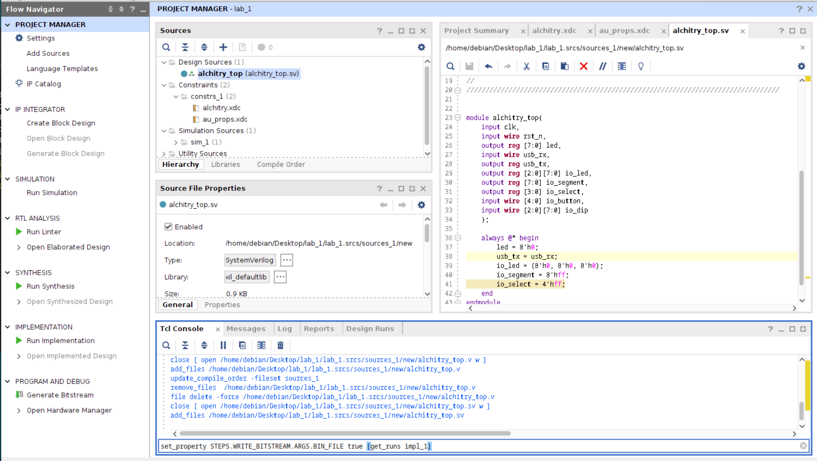
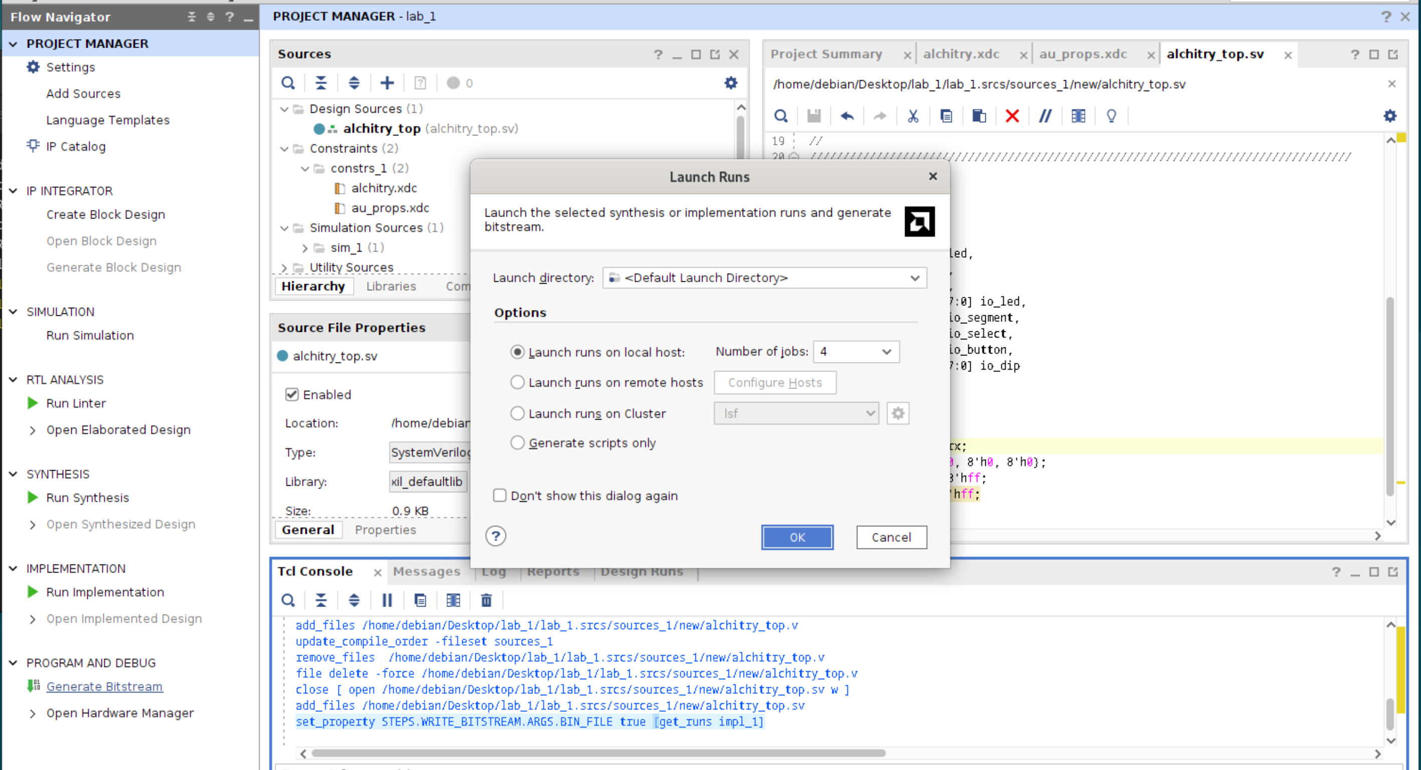
Generate Bitstream
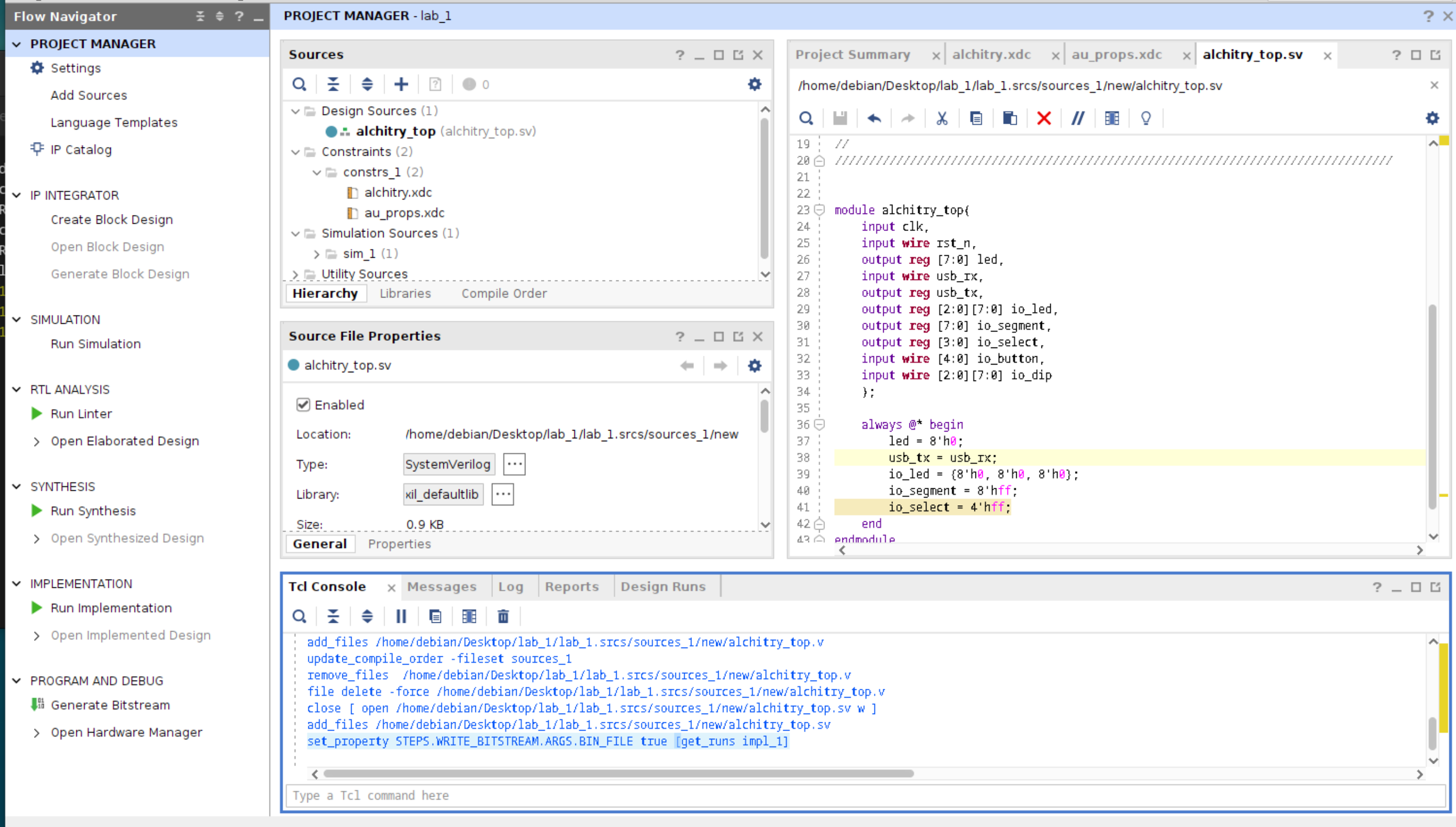
To test compile your RTL, go to the TCL Console and type the command:
set_property STEPS.WRITE_BITSTREAM.ARGS.BIN_FILE true [get_runs impl_1]
It tells Vivado to generate a .bin file in addition to the .bit file during the write_bitstream step of the impl_1 implementation run.
Press enter, and you should see the command taking effect:
Finally, click the Generate Bitstream under Flow Navigator: Program and Debug, then press OK:
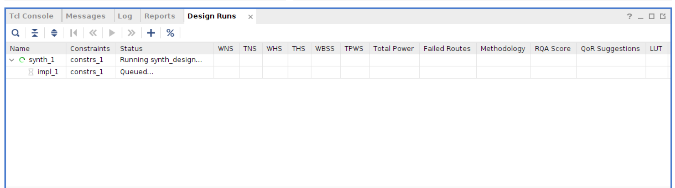
You should see that Vivado is running to synthesize your design under Design Runs:
Once completed, you should see this window. You can view the report if you want to.
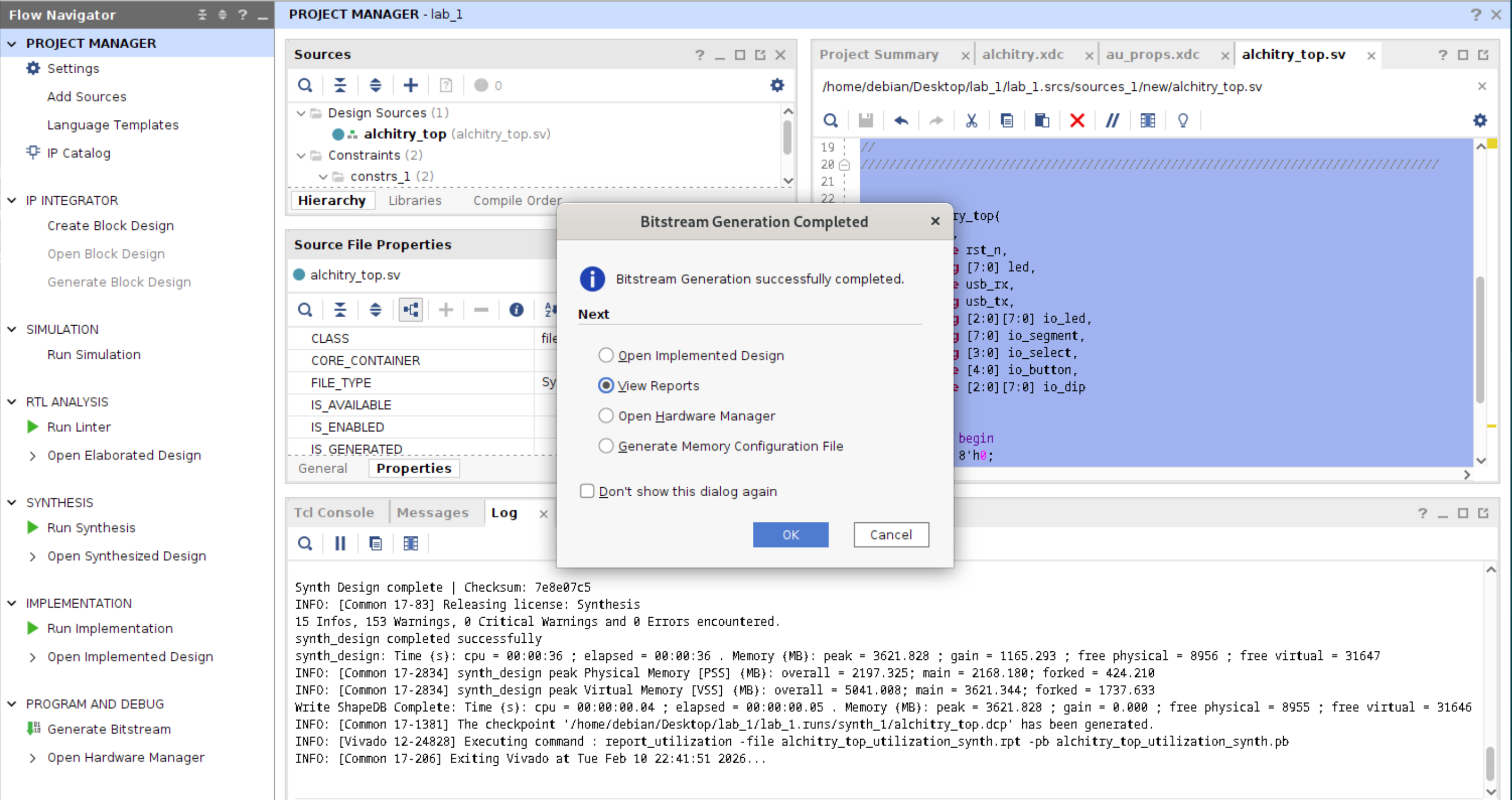
If your design failed for whatever reason, open the Log tab and inspect.
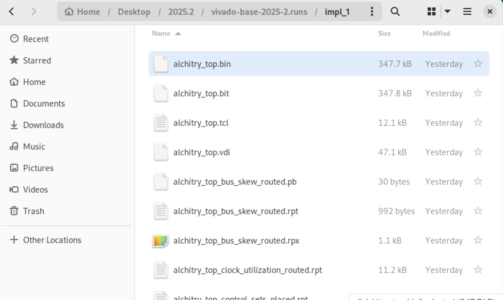
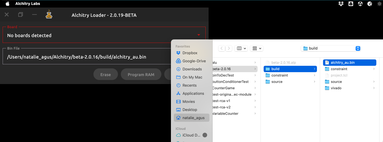
Load .bin File to Alchitry Au
The generated alchitry.bin file can be found under the directory <PROJECT_DIR>/<PROJECT_NAME>.runs/impl_1/alchitry_top.bin:
Use Alchitry Labs to load the binary to your FPGA. If you don’t have it yet, install from here. When you open the app, switch to Alchitry Loader first:
Find the synthesized binary and load it to your Alchitry Au FPGA:
Creating Design Sources in Verilog
The top file alchitry_top is written in System Verilog, which has lots of upgrades like multi-dimensional ports. It is handy in our case, since io_led and io_dip are defined in the constraint files as multi-dimensional ports.
Verilog (often “Verilog-2001/2005” in FPGA flows) is the older HDL. The labs are all written in Verilog for educational and simplicity purposes. Because of this, we need to “bridge” the top module with the verilog version.
Bridge Top Module
Create another design source called alchitry_top_verilog.v:
`timescale 1ns / 1ps

module alchitry_top_verilog(
    input        clk,
    input        rst_n,
    output reg [7:0] led,
    input        usb_rx,
    output reg   usb_tx,

    // Flattened io_led[2:0][7:0] into 24 bits:
    // [7:0]   = io_led[0]
    // [15:8]  = io_led[1]
    // [23:16] = io_led[2]
    output reg [23:0] io_led_flat,

    output reg [7:0]  io_segment,
    output reg [3:0]  io_select,
    input      [4:0]  io_button,

    // Flattened io_dip[2:0][7:0] into 24 bits:
    // [7:0]   = io_dip[0]
    // [15:8]  = io_dip[1]
    // [23:16] = io_dip[2]
    input      [23:0] io_dip_flat
);

  always @* begin
    led         = 8'h00;
    usb_tx      = usb_rx;
    io_led_flat = 24'h000000;
    io_segment  = 8'hFF;
    io_select   = 4'hF;
  end

endmodule
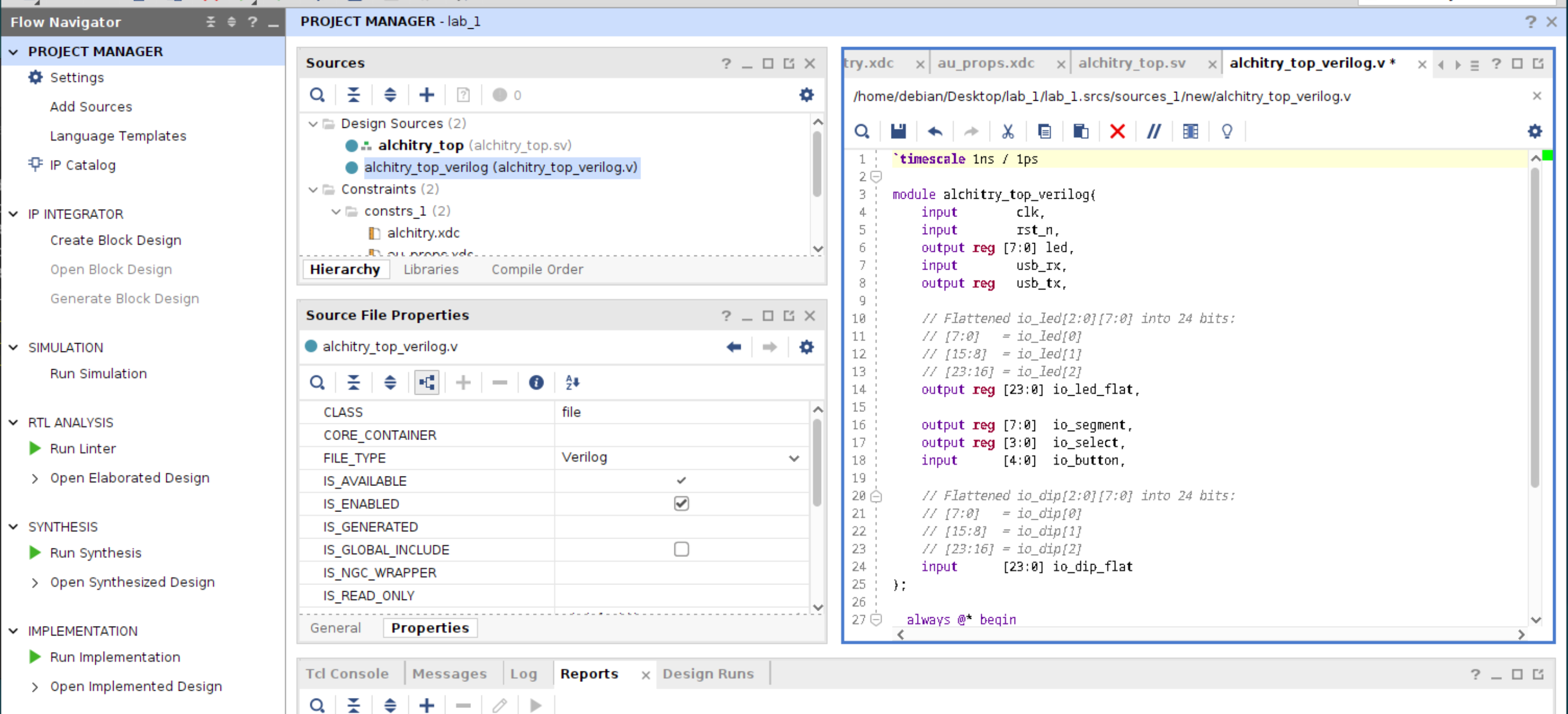
This is a bridging module that flattens the multi-dimensional ports io_led and io_dip.
Then edit alchitry_top.sv to wrap over this module:
module alchitry_top(
    input  logic clk,
    input  logic rst_n,
    output logic [7:0] led,
    input  logic usb_rx,
    output logic usb_tx,
    output logic [2:0][7:0] io_led,
    output logic [7:0] io_segment,
    output logic [3:0] io_select,
    input  logic [4:0] io_button,
    input  logic [2:0][7:0] io_dip
);

  // pack SV arrays into flat vectors for the Verilog-2005 module
  wire [23:0] io_dip_flat = { io_dip[2], io_dip[1], io_dip[0] };
  wire [23:0] io_led_flat;

  // unpack flat vector back into SV array
  assign { io_led[2], io_led[1], io_led[0] } = io_led_flat;

  alchitry_top_verilog u_core (
    .clk(clk),
    .rst_n(rst_n),
    .led(led),
    .usb_rx(usb_rx),
    .usb_tx(usb_tx),
    .io_led_flat(io_led_flat),
    .io_segment(io_segment),
    .io_select(io_select),
    .io_button(io_button),
    .io_dip_flat(io_dip_flat)
  );

endmodule
Then from now onwards, you only modify alchitry_top.v and connect it with your datapath’s top module accordingly, and leave the System Verilog alchitry_top.sv alone.
Reset and Button Conditioners
If you are developing your project entirely in Verilog, using Vivado or editor of your choice, you need to implement your own libraries like Reset and Button Conditioners that were originally provided by Alchitry Labs.
Here’s a suggested implementation (taken from Alchitry Lab’s automatic build, which you can find under <PROJECT_DIR>/build/src folder).
Reset Conditioner
System Verilog
// reset_conditioner.sv
/*
    This file was generated automatically by Alchitry Labs 2.0.52-BETA.
    Do not edit this file directly. Instead edit the original Lucid source.
    This is a temporary file and any changes made to it will be destroyed.
*/

module reset_conditioner #(
        parameter STAGES = 3'h4
    ) (
        input wire clk,
        input wire in,
        output reg out
    );
    logic [(STAGES)-1:0] D_stage_d, D_stage_q = {STAGES{1'h1}};
    always @* begin
        D_stage_d = D_stage_q;

        D_stage_d = {D_stage_q[(($bits(STAGES) > $bits(2'h2) ? $bits(STAGES) : $bits(2'h2)) + 1)'(STAGES - 2'h2):1'h0], 1'h0};
        out = D_stage_q[(($bits(STAGES) > $bits(1'h1) ? $bits(STAGES) : $bits(1'h1)) + 1)'(STAGES - 1'h1)];
    end


    always @(posedge (clk) or posedge (in)) begin
        if ((in) == 1'b1) begin
            D_stage_q <= {STAGES{1'h1}};
        end else begin
            D_stage_q <= D_stage_d;
        end
    end
endmodule
Verilog
`timescale 1ns / 1ps

module reset_conditioner #(
    parameter integer STAGES = 4
) (
    input  wire clk,
    input  wire in,
    output reg  out
);

  reg [STAGES-1:0] stage_q;

  // Combinational out is MSB of the shift register
  always @* begin
    out = stage_q[STAGES-1];
  end

  // Async assert, sync deassert (shift zeros in)
  always @(posedge clk or posedge in) begin
    if (in) begin
      stage_q <= {STAGES{1'b1}};
    end else begin
      stage_q <= {stage_q[STAGES-2:0], 1'b0};
    end
  end

endmodule
Button Conditioner
System Verilog
// button_conditioner.sv
/*
    This file was generated automatically by Alchitry Labs 2.0.52-BETA.
    Do not edit this file directly. Instead edit the original Lucid source.
    This is a temporary file and any changes made to it will be destroyed.
*/

module button_conditioner #(
        parameter CLK_FREQ = 27'h5f5e100,
        parameter MIN_DELAY = 5'h14,
        parameter NUM_SYNC = 2'h2
    ) (
        input wire clk,
        input wire in,
        output reg out
    );
    localparam _MP_DEPTH_1956405930 = NUM_SYNC;
    logic M_sync_in;
    logic M_sync_out;

    pipeline #(
        .DEPTH(_MP_DEPTH_1956405930)
    ) sync (
        .clk(clk),
        .in(M_sync_in),
        .out(M_sync_out)
    );


    logic [($clog2(($bits(CLK_FREQ)+$bits(MIN_DELAY))'(CLK_FREQ * MIN_DELAY) / 10'h3e8))-1:0] D_ctr_d, D_ctr_q = 0;
    always @* begin
        D_ctr_d = D_ctr_q;

        M_sync_in = in;
        out = (&D_ctr_q);
        if (!(&D_ctr_q)) begin
            D_ctr_d = (($bits(D_ctr_q) > $bits(1'h1) ? $bits(D_ctr_q) : $bits(1'h1)) + 1)'(D_ctr_q + 1'h1);
        end
        if (!M_sync_out) begin
            D_ctr_d = 1'h0;
        end
    end


    always @(posedge (clk)) begin
        D_ctr_q <= D_ctr_d;

    end
endmodule
Verilog
`timescale 1ns / 1ps

module button_conditioner #(
    parameter integer CLK_FREQ  = 100000000,  // Hz
    parameter integer MIN_DELAY = 20,         // ms
    parameter integer NUM_SYNC  = 2
) (
    input  wire clk,
    input  wire in,
    output reg  out
);


  function integer clog2;
    input integer value;
    integer v;
    begin
      v = value - 1;
      clog2 = 0;
      while (v > 0) begin
        v = v >> 1;
        clog2 = clog2 + 1;
      end
      if (clog2 < 1) clog2 = 1;
    end
  endfunction

  // Target cycles for MIN_DELAY ms (rounded down). Ensure >= 1.
  localparam integer TARGET_CYCLES_RAW = (CLK_FREQ / 1000) * MIN_DELAY;
  localparam integer TARGET_CYCLES = (TARGET_CYCLES_RAW < 1) ? 1 : TARGET_CYCLES_RAW;

    `ifdef SIM
    // Fast debounce for sim: 4 cycles to reach all-ones if CTR_W=2
    localparam integer CTR_W = 2;
    `else
    localparam integer CTR_W = clog2(TARGET_CYCLES);
    `endif

  // -----------------------------
  // Synchronizer chain
  // -----------------------------
  reg [NUM_SYNC-1:0] sync_ff;
  integer k;

  always @(posedge clk) begin
    sync_ff[0] <= in;
    for (k = 1; k < NUM_SYNC; k = k + 1) begin
      sync_ff[k] <= sync_ff[k-1];
    end
  end

  wire in_sync = sync_ff[NUM_SYNC-1];

  // -----------------------------
  // Debounce counter
  // -----------------------------
  reg [CTR_W-1:0] ctr;

  always @(posedge clk) begin
    if (!in_sync) begin
      ctr <= {CTR_W{1'b0}};
    end else if (!(&ctr)) begin
      ctr <= ctr + { {(CTR_W - 1) {1'b0} }, 1'b1};
    end
    out <= &ctr;
  end

endmodule
Usage
A Verilog-2005 (.v) module can instantiate a SystemVerilog (.sv) module as long as Vivado compiles both into the same design and the port list matches.
For example, suppose we create reset_conditioner.sv, just use it like so inside alchitry_top_verilog.v:
wire rst_cond; // conditioned active low reset
wire rst = ~rst_cond; // invert to obtain active high


reset_conditioner u_reset_conditioner(
    .clk(clk),
    .in(rst_n),
    .out(rst_cond)
)
Similarly with button conditioner:
  wire btn_raw;
  wire btn_clean;

  button_conditioner #(
    .CLK_FREQ(27'h5f5e100),
    .MIN_DELAY(5'h14),
    .NUM_SYNC(2'h2)
  ) u_bc (
    .clk(clk),
    .in(btn_raw),
    .out(btn_clean)
  );
Reset Runs
Do not forget to reset synth_1 runs as necessary when you edit the source files before generating new bitstream.
Viewing LUTs Usage
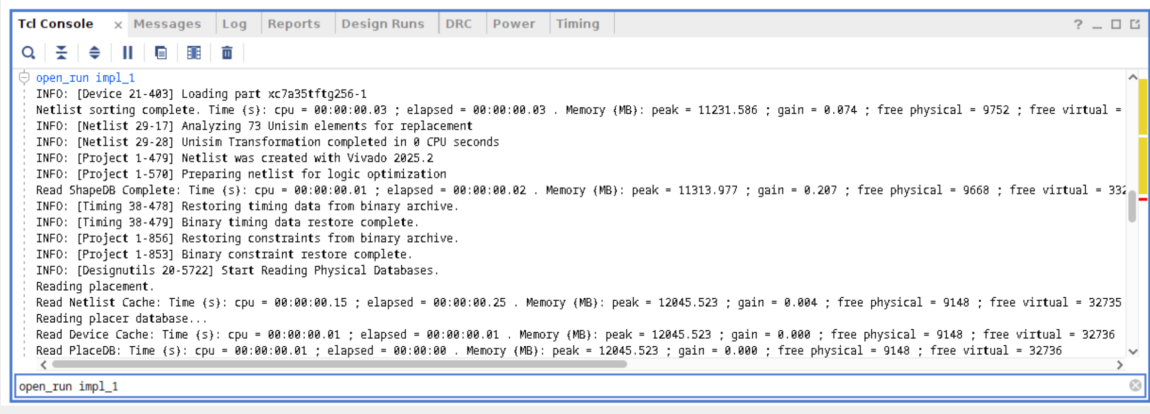
Once implementation is complete, you can double click on impl_1, this will open the netlist. Alternatively, go to Tcl Console and type open_run impl_1:
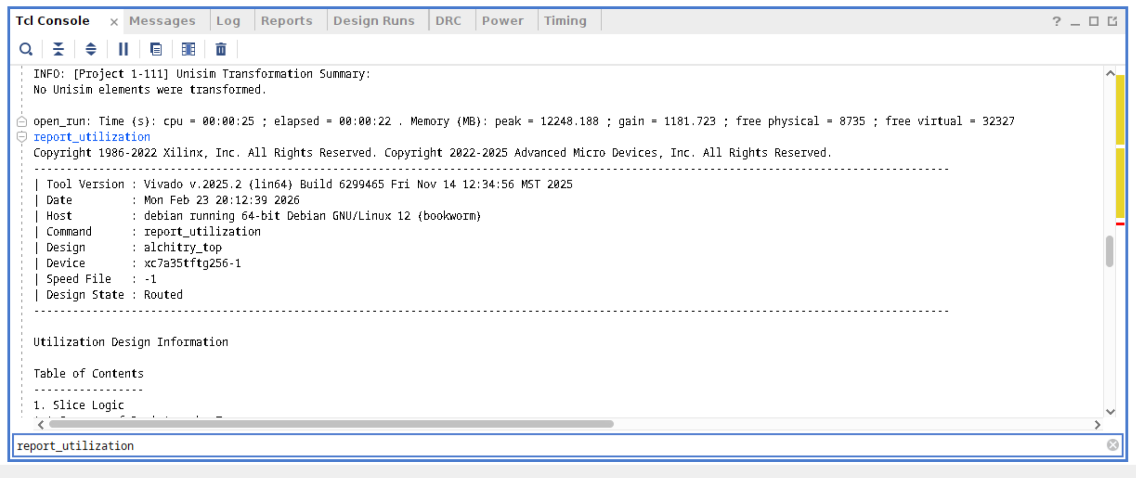
Afterwards, type the command report_utilization:
Then scroll down to Slice Logic:
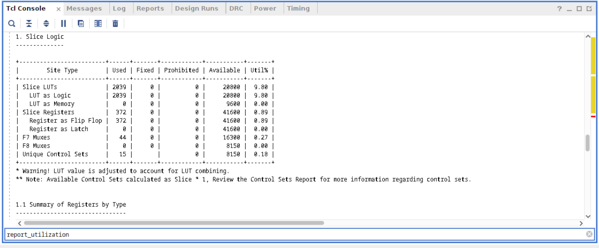
This report shows that we only use 9.80% of the Slice LUTs, which just a small amount.
Timing Summary
Design Runs typically also report timing constraints. WNS and TNS are the important ones:
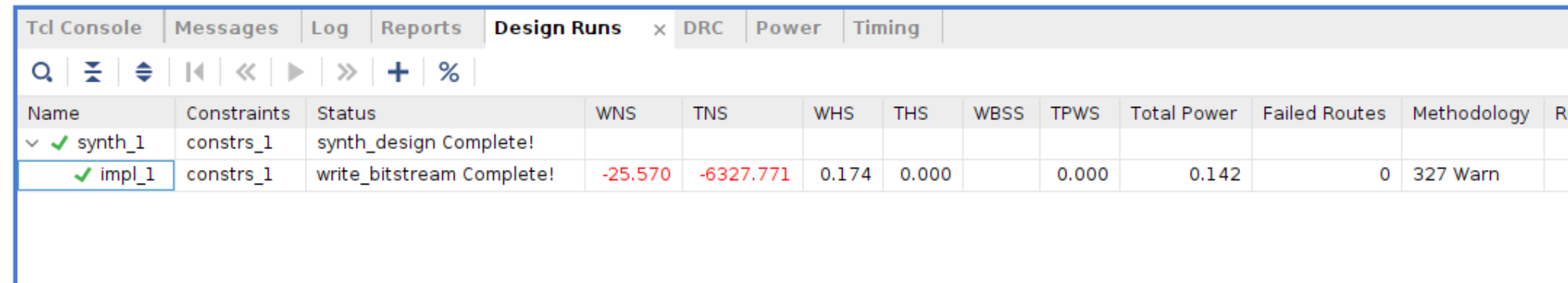
WNS: Worst Negative Slack
- The single worst setup timing slack in the design
- >= 0 ns means setup timing meets for all analyzed paths
- < 0 ns means timing violation exists (you are late by that amount on the worst path)
TNS: Total Negative Slack
- Sum of negative setup slack across failing endpoints
- 0 ns means no setup violations
- More negative means broader timing problems, not just one bad path
TLDR: if you see these numbers in red, you are in trouble. You might want to insert dff in the violating paths or reduce the clock frequency.
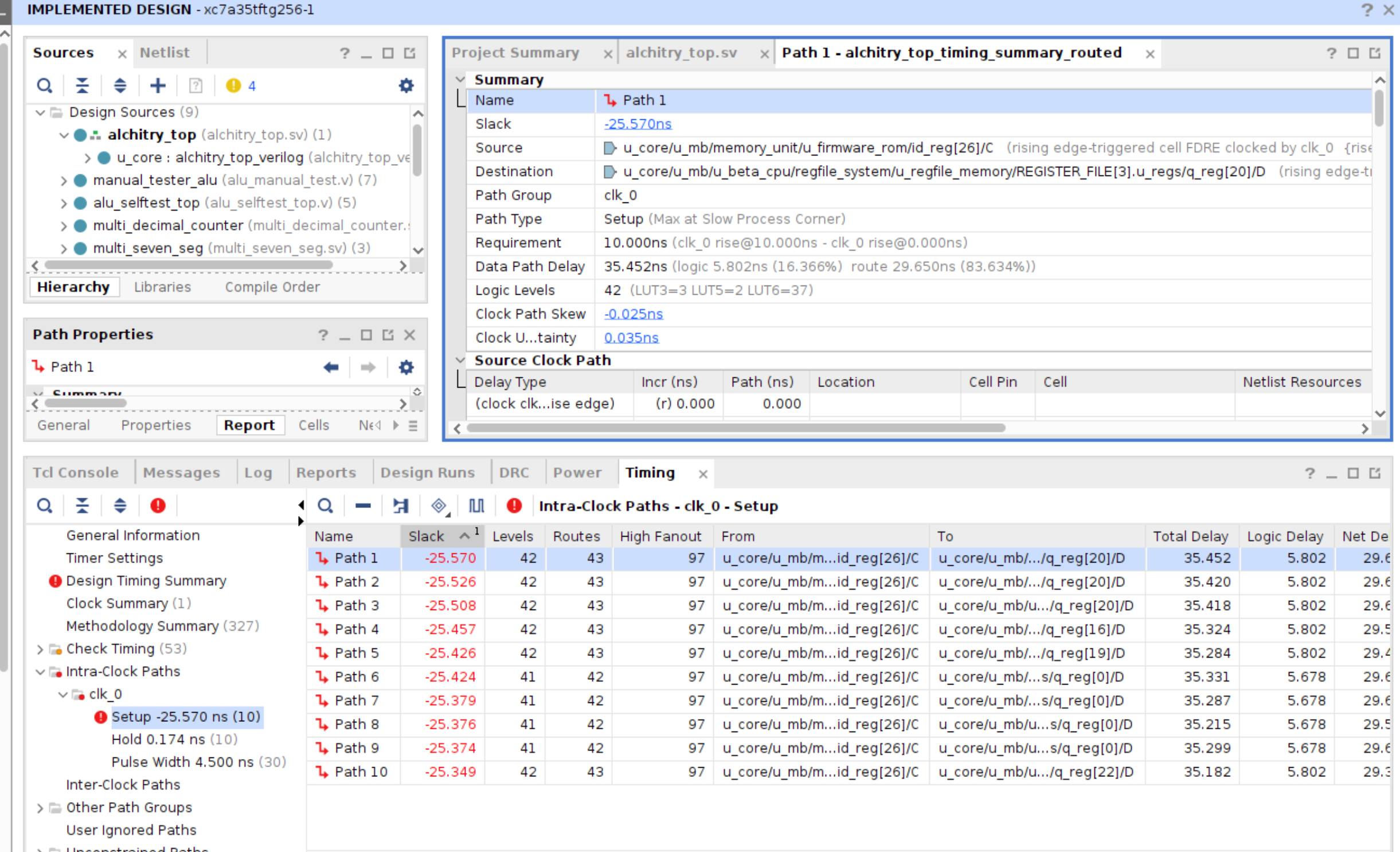
To find out the violating paths, open the Timing Window and view the Intra-Clock Paths:
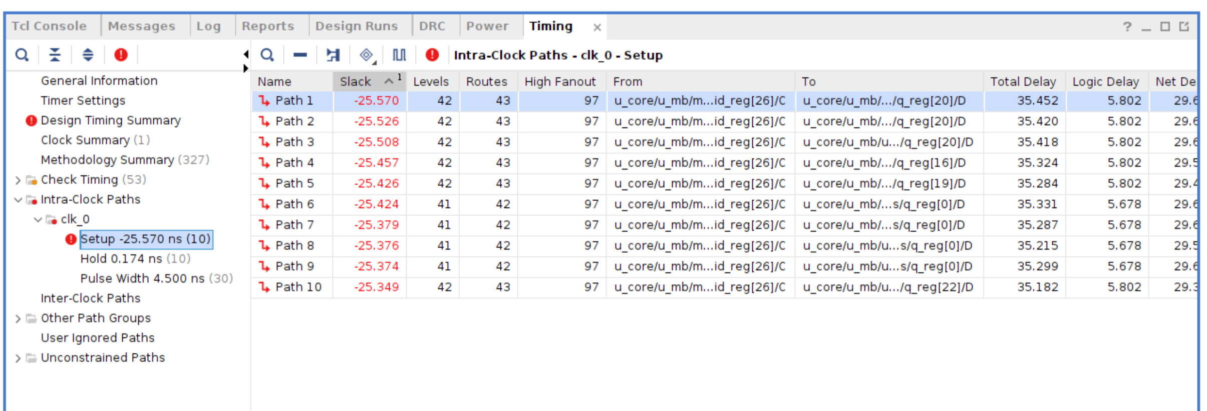
The table reports:
- Worst setup slack = -25.570 ns which is very bad
- Levels = 42 means about 42 logic stages on the path (very deep)
- High Fanout = 97 also hurts timing
- Total Delay ~35.45 ns
- Logic Delay ~5.8 ns
You can then click on the path to inspect it further:
Immediate fixes you can do that’s suitable for 50.002 projects:
- break long combinational chain with pipeline registers, this increases latency but shouldn’t be an issue
- Edit the control logic to consider the edges of slower internal clock (a level slow counter passed through an edge-detector)
AI/Google searches might suggest you to do:
- reduce fanout on heavily-used control signals (google this)
- register outputs of large mux trees (google this)
These are absolutely overkill for school projects. Resort to method 1 & 2 above instead.