50.002 Computation Structures
Information Systems Technology and Design
Singapore University of Technology and Design
Alchitry Pinout
This handout is written for you to understand how to connect external I/O devices to your Alchitry boards.
For your 1D project, we give you 3 types of boards:
- Alchitry Au (the FPGA) V1 (not V2!)
- Alchitry Br
- Alchitry Io
They are stacked on top of one another, and custom “wings” have been created by us to enable usage of the Br board with the Io board.
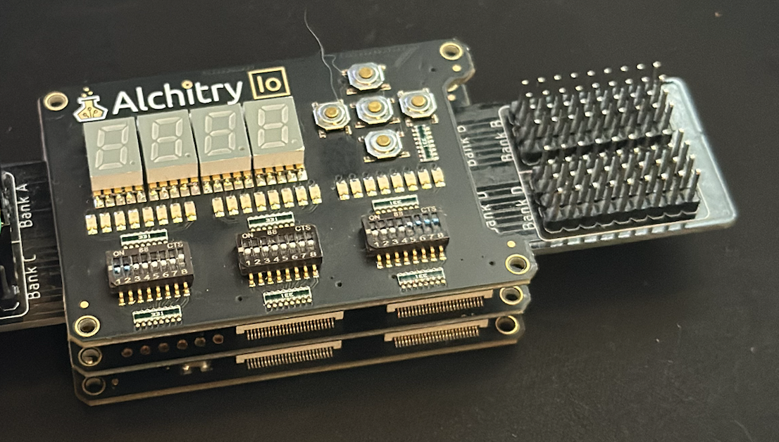
We bought the V1 version
If you head to Alchitry website, you see that there are V2 versions of Au, Br, and Io. We do not use these. We are using the V1 version (bought from Sparkfun)
Alchitry Br
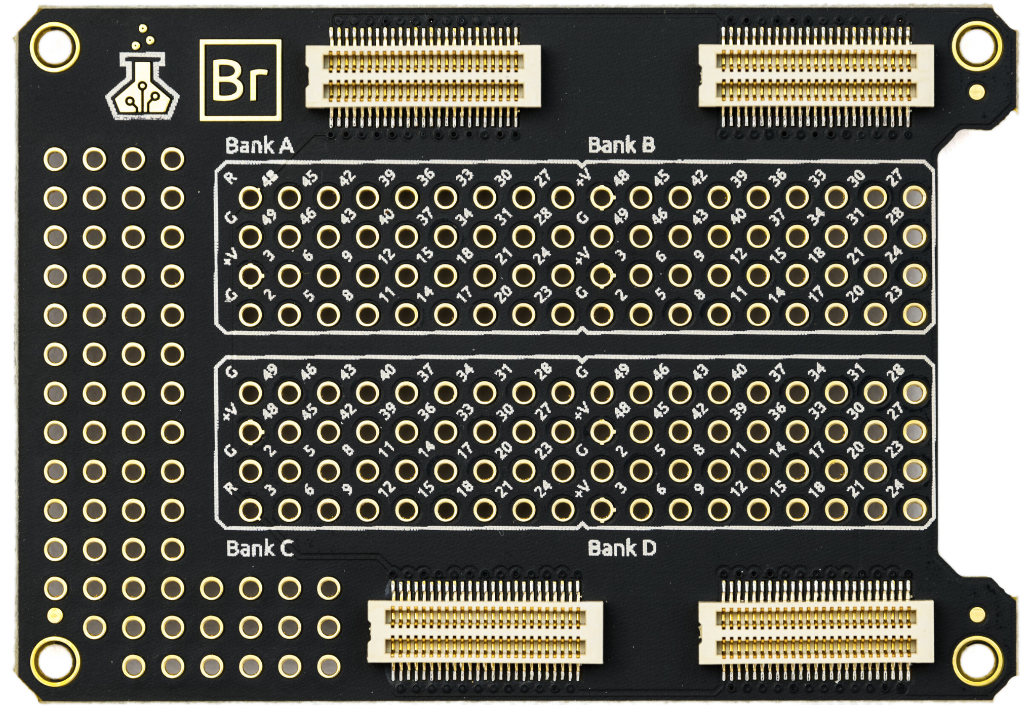
The Alchitry Br Element Board is a prototyping periphery for the Au board. The Br breaks out all the signals on the four headers running from your Au. It has a large prototyping area with a 0.1” pin grid for custom circuits. We built custom wings on the Br so you can easily use jumper wires for your electronic prototype without having to solder anything to the board.
Alchitry Io
The Io is similar to Arduino shields, but for the Au board instead. It features four 7-segment LEDs, five momentary push buttons, 24 basic LEDs, and 24 DIP switches for instant and easy testing.
Motivation
Once you ensure that your project works in simulation, you need to ensure that it works in hardware. There are two steps to this process:
- Ensure that it works on the FPGA with the Io Board (straightforward)
- Ensure that it works on the FPGA + external connections (actual LEDs, external 7segments) via the Br Board
This guide is written to highlight how we can map logical design signals (e.g., io_led, io_dip) to specific physical pins on the FPGA board like A24, B3, etc.
The Constraint File
To understand the constraint file, create a new project with Alchitry Au Board and Io Demo V1 with pulldown as the template.
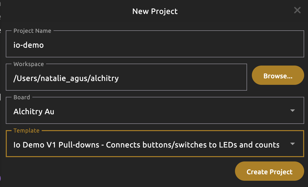
Do not use the V2 board / template.
You should see the file alchitry_top.luc, which is the “main” file for the project. Logical I/O is defined at the top:
module alchitry_top (
    input clk,              // 100MHz clock
    input rst_n,            // reset button (active low)
    output led[8],          // 8 user controllable LEDs
    input usb_rx,           // USB->Serial input
    output usb_tx,          // USB->Serial output
    output io_led[3][8],    // LEDs on IO Shield
    output io_segment[8],   // 7-segment LEDs on IO Shield
    output io_select[4],    // Digit select on IO Shield
    input io_button[5],     // 5 buttons on IO Shield
    input io_dip[3][8]      // DIP switches on IO Shield
)
Each of these logical design signals is mapped to specific physical pin on the FPGA board. This mapping is defined in the .acf file. There are two .acf files: alchitry.acf and io_v1_pullfown.acf.
alchitry.acf
// alchitry.acf
STANDARD(LVCMOS33) {
    pin clk CLOCK FREQUENCY(100MHz)

    pin rst_n RESET

    pin led[0] LED0
    pin led[1] LED1
    pin led[2] LED2
    pin led[3] LED3
    pin led[4] LED4
    pin led[5] LED5
    pin led[6] LED6
    pin led[7] LED7

    pin usb_rx USB_RX
    pin usb_tx USB_TX
}
alchitry.acf maps the logical signals led and usb_rx/tx, clk, and rst to the corresponding physical pin (LED0, RESET, etc) on the Alchitry Au FPGA board. Notice the standard LVCMOS33. This is a specific I/O standard used in FPGA designs for interfacing with external devices. It stands for:
- LVCMOS: Low-Voltage Complementary Metal-Oxide-Semiconductor.
- 33: Specifies the voltage level of 3.3 volts.
- High Voltage (VOH): Typically close to 3.3V.
- Low Voltage (VOL): Close to 0V.
- Operates reliably at a supply voltage of 3.3V.
That means the FPGA I/O pin can supply voltages within the range defined by the 3.3V logic levels, but not necessarily exactly 3.3V at all times. It is designed to be sufficient for devices that expect 3.3V CMOS signaling.
Constraint Format
The constraint format is as follows:
pin PORT PIN OPTIONAL_ATTRIBUTES
PORT is a logical port name from your design’s top-level module (alchitry_top.luc) and PIN is the physical Alchitry pin to connect it to.
Most of the time, the PIN name will follow a format of bank letter followed by the pin number like A2 for bank A pin 2. However, there are special values such as LED0 which corresponds to the pin connected to the first LED on the Au board.
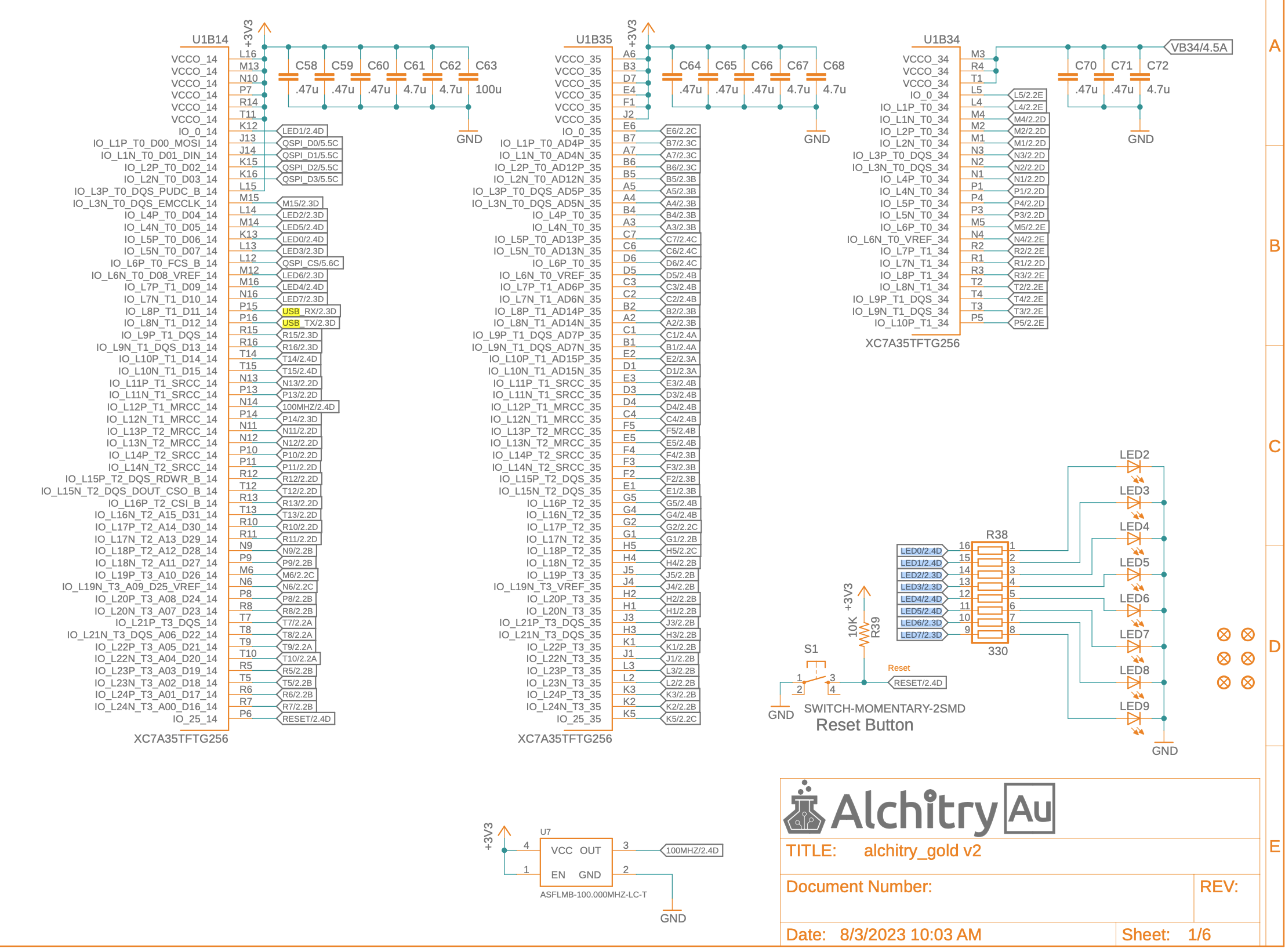
Alchitry Au V1 schematic clearly shows the physical name of the pins on the Au Board:
io.acf (v1 pulldown, name might vary)
The IO constraint file outlines the mapping between the logical ports in alchitry_top.luc and the physical Alchitry pin on the banks. There are four banks in Alchitry Au V1:
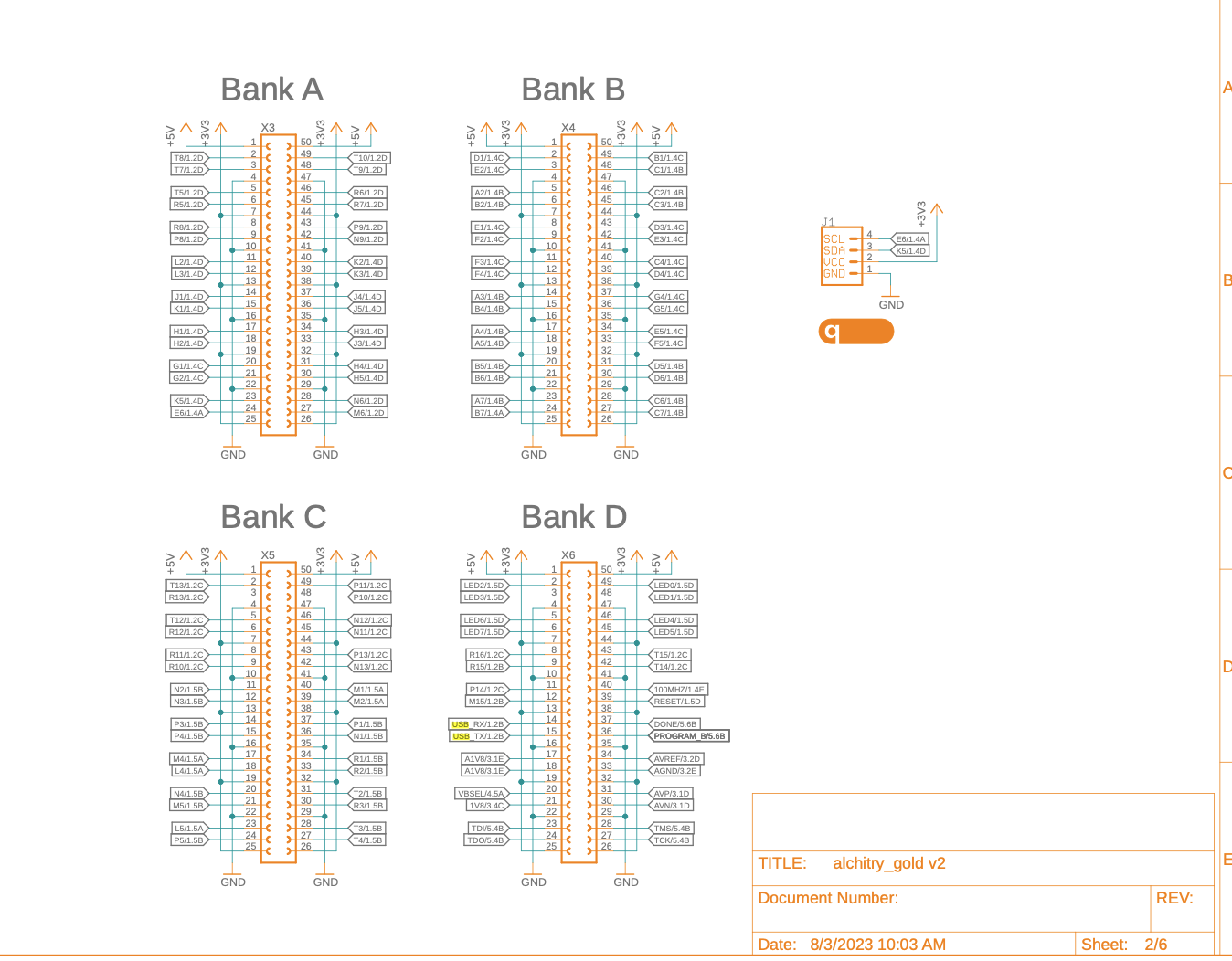
The Br breakout board allows you to connect external I/O devices to the Alchitry Au FPGA. It provides access to the four I/O banks available on the Au, and you can directly solder connections to the breakout board for prototyping purposes.
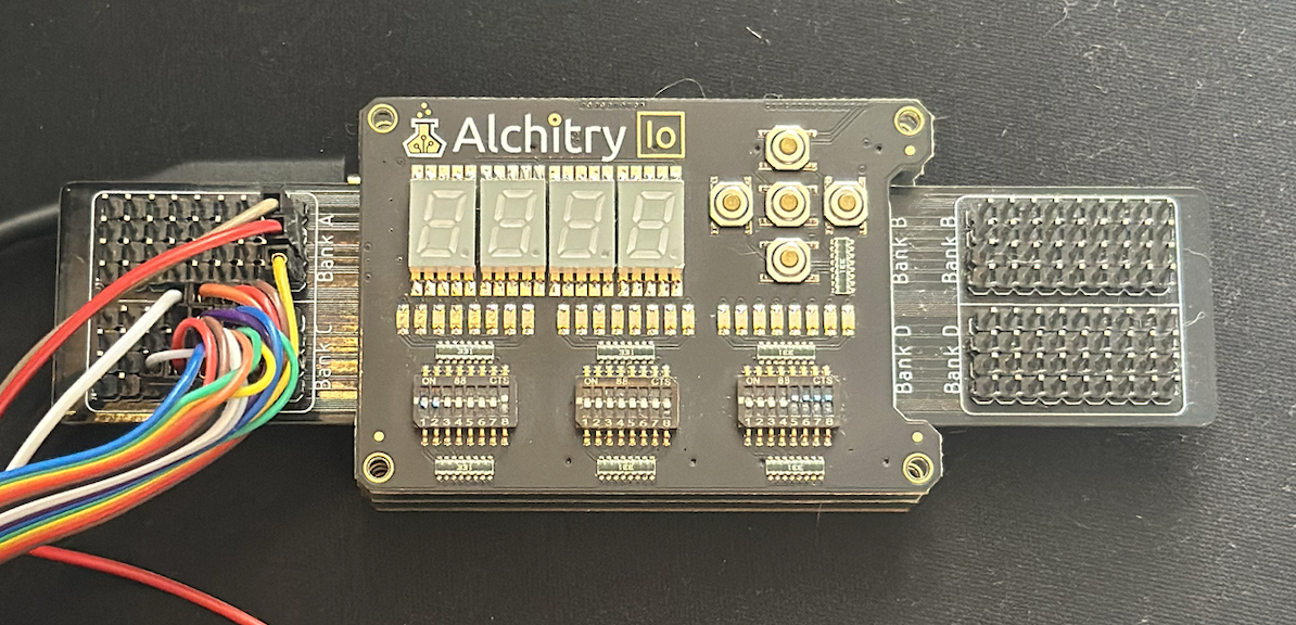
Custom Br Wings
Our custom “wings” enable you to connect external IOs to it using jumper wires instead of having to solder to it:
Br Element Reference Card
You should utilise this reference card for your project. Save this image.
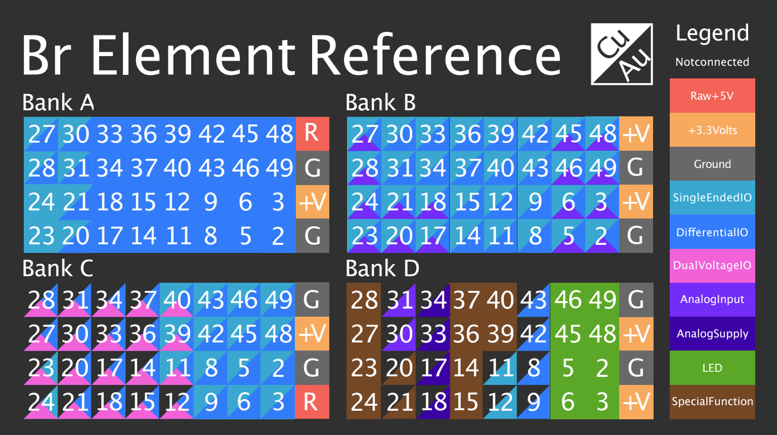
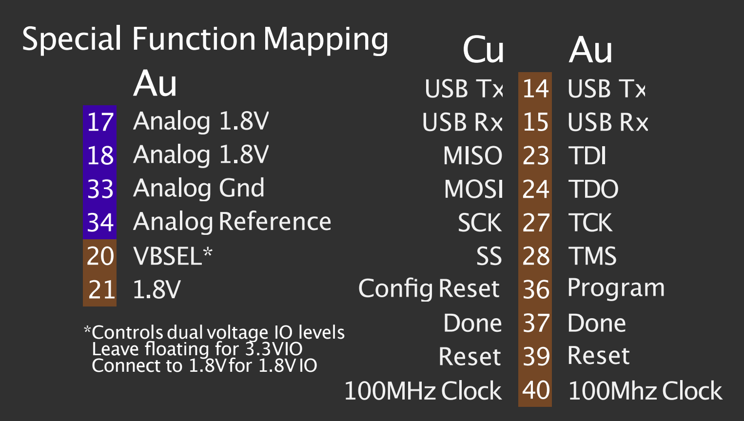
Overlay this card on the Br wings to figure out the pin numbering.
For instance, here’s a few of Bank B pin names:

Various I/O functionalities
These pin types define the electrical and functional characteristics of the available connections. They provide flexibility to interface with a wide range of external components or peripherals.
You can use Single-Ended I/O, Differential I/O, or Dual Voltage IO as General Purpose IO (GPIO) in most FPGA designs.
Consult the appendix if you’d like to use other types (not common for 50.002 project).
Version 1 Pulldownio.acf
The v1 constraint file that comes with this template has a pulldown attribute set. The content is as follows:
// io_v1_pulldown.acf

PINOUT(V1), STANDARD(LVCMOS33) {
    pin io_led[0][0] B21
    pin io_led[0][1] B20
    pin io_led[0][2] B18
    pin io_led[0][3] B17
    pin io_led[0][4] B15
    pin io_led[0][5] B14
    pin io_led[0][6] B12
    pin io_led[0][7] B11
    pin io_led[1][0] B9
    pin io_led[1][1] B8
    pin io_led[1][2] B6
    pin io_led[1][3] B5
    pin io_led[1][4] B3
    pin io_led[1][5] B2
    pin io_led[1][6] A24
    pin io_led[1][7] A23
    pin io_led[2][0] A21
    pin io_led[2][1] A20
    pin io_led[2][2] A18
    pin io_led[2][3] A17
    pin io_led[2][4] A15
    pin io_led[2][5] A14
    pin io_led[2][6] A12
    pin io_led[2][7] A11

    PULL(DOWN) {
        pin io_dip[0][0] B30
        pin io_dip[0][1] B31
        pin io_dip[0][2] B33
        pin io_dip[0][3] B34
        pin io_dip[0][4] B36
        pin io_dip[0][5] B37
        pin io_dip[0][6] B39
        pin io_dip[0][7] B40
        pin io_dip[1][0] B42
        pin io_dip[1][1] B43
        pin io_dip[1][2] B45
        pin io_dip[1][3] B46
        pin io_dip[1][4] B48
        pin io_dip[1][5] B49
        pin io_dip[1][6] A27
        pin io_dip[1][7] A28
        pin io_dip[2][0] A30
        pin io_dip[2][1] A31
        pin io_dip[2][2] A33
        pin io_dip[2][3] A34
        pin io_dip[2][4] A36
        pin io_dip[2][5] A37
        pin io_dip[2][6] A39
        pin io_dip[2][7] A40

        pin io_button[0] B28
        pin io_button[1] B27
        pin io_button[2] B23
        pin io_button[3] B24
        pin io_button[4] C49
    }

    pin io_select[0] A9
    pin io_select[1] A8
    pin io_select[2] A42
    pin io_select[3] A43

    pin io_segment[0] A5
    pin io_segment[1] A6
    pin io_segment[2] A48
    pin io_segment[3] A46
    pin io_segment[4] A45
    pin io_segment[5] A3
    pin io_segment[6] A2
    pin io_segment[7] A49
}
Pulldown (for input pins)
Notice the attribute block PULL(DOWN) in the constraint file above. This block applies pin pulldown to the same bunch of pins. These are input pins.
Pin pulldown
Physically, a pin pulldown refers to a resistor that is connected between a GPIO pin and ground to ensure that the pin reads a low logic level (0) when it is not actively driven by an external signal.
In an FPGA, a pulldown is typically implemented using an internal pulldown resistor that can be configured in the design software.
Below is a simple schematic illustrating a physical pulldown (and equivalently, pullup) resistor:
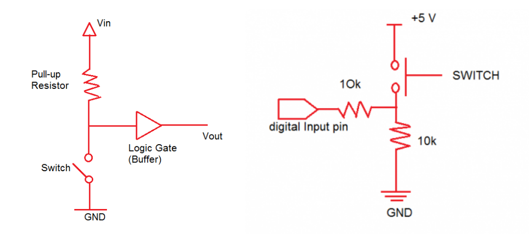
The reason we need a pulldown attribute here is because io_dip and io_button are inputs. If a GPIO pin is configured as an input and not connected to an external signal, a pulldown ensures the pin reads 0 instead of an undefined “floating” state.
Without pulldown: “float”
Without a pulldown, an unpressed io_button or an “off” io_switch will not give logic 0. The pin is said to “float,” meaning it may pick up electrical noise or stray signals from the environment, causing unpredictable behavior.
Further documentation
You typically will not need to know more about the syntax of the constraint files beyond what’s already given as samples in the template. However further details can be read here.
Connecting External I/O
The behavior of this sample project is simple: io_led mirrors io_dip:
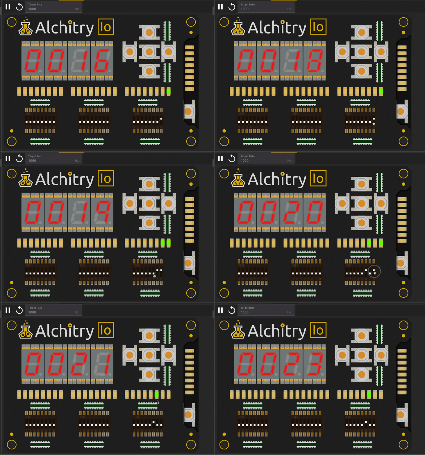
In the constraint file, io_led[0][0] is connected to Br pin B21, io_led[0][1] to B20 and so on.
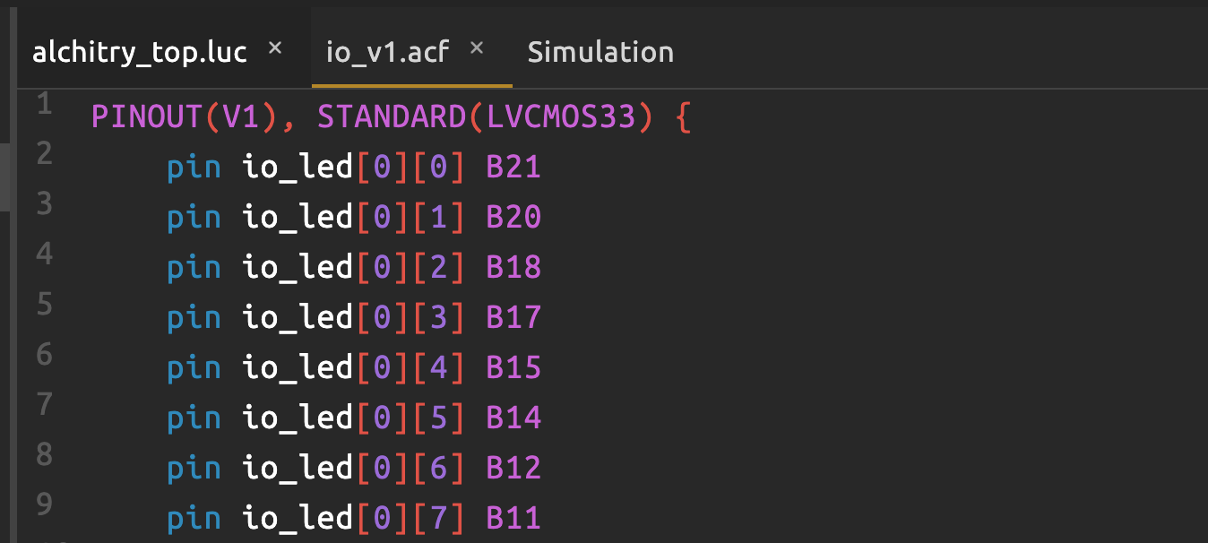
Therefore, if you want to connect external LED bulbs to mirror io_led[0][0] and io_led[0][1], simply connect the anode legs (longer leg) to B21 and B20 + resistor in between, and the cathode leg (shorter leg) to any of the GND pin.

Summary
We briefly goes through how to connect external I/O units to the FPGA, in particular: how the .acf file works and understanding how pulldown works.
If your project works fine in the simulator but haywires in build, check if the constraints with pulldown is used. Otherwise, your inputs will be “floating” and it causes your FSM to behave unpredictably (triggered when no button / switch is pressed, etc).
Remember to use our custom Br Reference Card when utilising the wings.
Appendix
 Here’s the breakdown of what each IO type stated in the Br Element Reference represents:
- Raw +5V:
- Description: A pin that supplies a raw, unregulated 5V voltage directly from the power source.
- Use Case: Powering external components or circuits that require 5V. Be cautious when using it, as it may not be regulated or protected.
- Single-ended IO (most commonly used)
- Description: Standard digital I/O pins that operate with respect to a common ground. Each signal is carried on a single wire.
- Use Case: General-purpose digital input/output for driving LEDs, reading button states, etc.
- Examples:
- GPIO pins on microcontrollers.
- Logic signals for basic components like sensors or switches.
- Differential IO:
- Description: I/O pins designed to transmit or receive signals in a differential pair, where two wires carry complementary signals.
- Use Case:
- High-speed or noise-resistant communication (e.g., LVDS, RS-485).
- Reduces electromagnetic interference (EMI) and increases signal integrity.
- Examples:
- Differential signaling for clocks or data lines (e.g., Ethernet, HDMI).
- Dual Voltage IO:
- Description: I/O pins that support multiple voltage levels, typically configured based on the connected device’s requirements.
- Use Case:
- Interfacing with components operating at different logic levels (e.g., 3.3V and 1.8V).
- Examples:
- FPGA I/O banks often support dual-voltage configurations using dedicated supply pins.
- Analog Input:
- Description: Pins that can read analog voltage levels and convert them to digital values using an ADC (Analog-to-Digital Converter).
- Use Case:
- Reading sensor data (e.g., temperature, light, or sound levels).
- Examples:
- Pins connected to ADC modules in microcontrollers like the Arduino or STM32.
- Analog Supply:
- Description: Dedicated power pins for providing clean and stable power to analog circuits.
- Use Case:
- Powering ADCs, DACs, or other analog subsystems that require reduced noise and stable operation.
- Examples:
- AVCC on microcontrollers or FPGA analog banks.
- LED:
- Description: Pins specifically designed to drive LEDs, often with built-in current-limiting or PWM support.
- Use Case:
- Driving status or indicator LEDs directly.
- Examples:
- FPGA or microcontroller pins labeled for onboard LEDs.
- Special Function:
- Description: Pins that can perform specific, pre-defined hardware functions (beyond general-purpose I/O).
- Use Case:
- Functions like SPI, I2C, UART, PWM, or clock generation.
- Examples:
- Pins labeled as SDA/SCL for I2C, TX/RX for UART.
 50.002 CS