 50.002 CS
- Control Sequencing with Finite State Machines
- Implementing a Controller–Datapath System in Verilog
- Slowing Down an FSM for Human Observation
- Run on FPGA
- Processing Button Presses
- Build Automated Register Adder Tester
- Summary
50.002 Computation Structures
Information Systems Technology and Design
Singapore University of Technology and Design
(Verilog) Lab 4: Control Sequencing
This is a Verilog parallel of the Lucid + Alchitry Labs Lab 4. It is not part of the syllabus, and it is written for interested students only. You still need to complete all necessary checkoffs in Lucid, as stated in the original lab handout.
If you are reading this document, we assume that you have already read Lab 4 Lucid version, as some generic details are not repeated. This lab has the same objectives and related class materials so we will not paste them again here. For submission criteria, refer to the original lab 4 handout.
Control Sequencing with Finite State Machines
In this lab, you are going to implement an FSM + Datapath, and write testbenches to ensure that the wirings are done properly. In particular, you are going to build an automated registered adder tester. Afterwards, you are going to build the project using Vivado, and load the binary to your FPGA using Alchitry Loader.
Installation
Vivado (free standard edition) and Alchitry Loader (part of Alchitry Labs) is required for this lab. Please install them. If you are using macOS, you cannot install Vivado on your system. Read alternatives here.
The Datapath
Following Lab 4 Lucid Version, the proposed datapath is as follows:

You are free to modify them but we are going to stick with implementing the above in this handout.
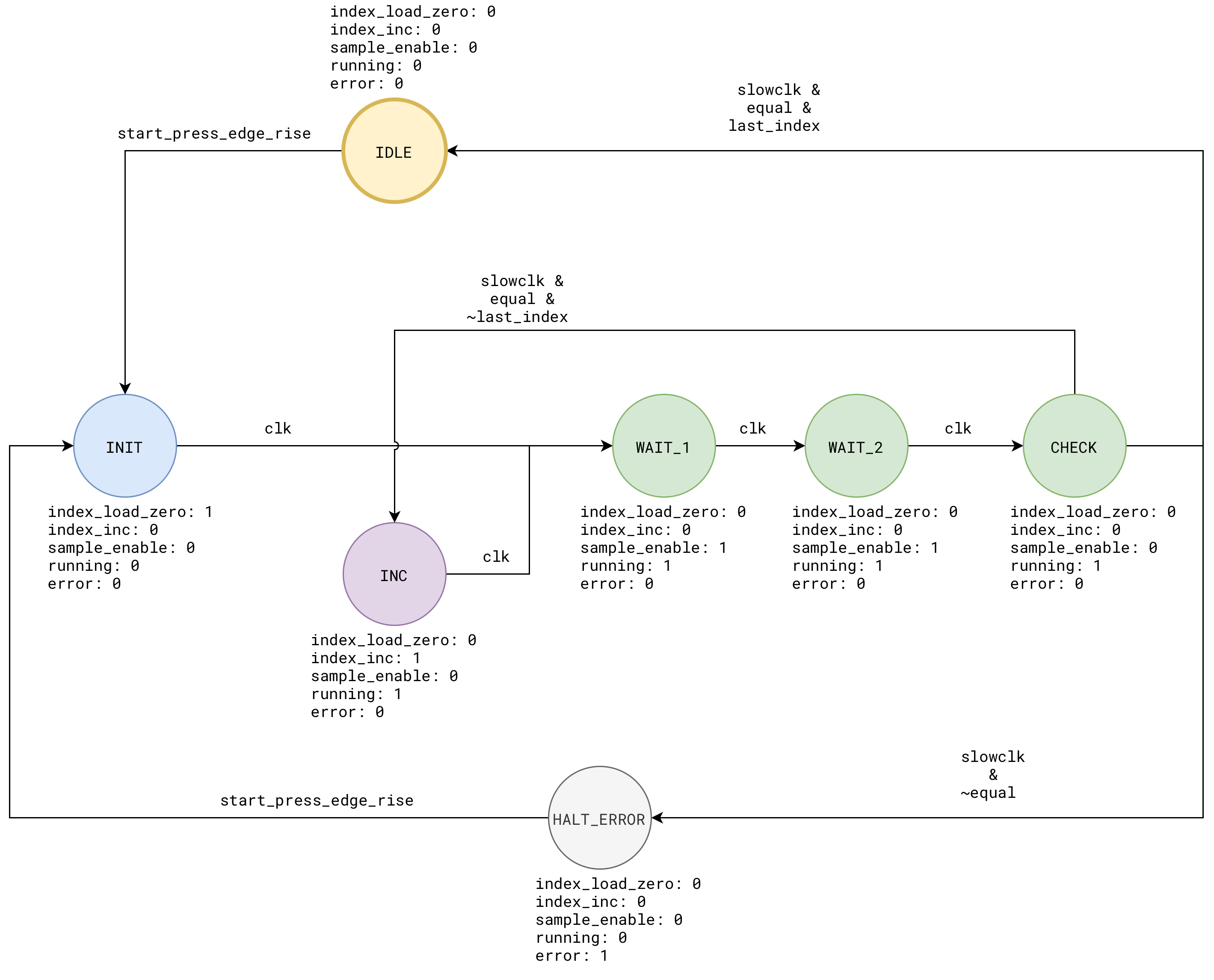
The FSM
The proposed FSM that will produce the control signals for the datapath is as follows:
The rest of this handout will touch on how we can implement the above in Verilog.
Implementing a Controller–Datapath System in Verilog
Recap: digital systems that do more than “pure combinational logic” usually have two different kinds of logic living together:
- Sequencing: deciding what happens first, next, and last.
- Computation and storage: holding values in registers and running arithmetic or comparisons on them.
A clean RTL structure (description of hardware in HDL like Verilog) separates these two roles.
The controller is none other than an FSM. It decides the sequence of steps. It outputs control signals such as ld_x, clr_x, sel_x, we, done, and so on.
The datapath contains the registers and the combinational logic between them. It performs the computation when the controller tells it to. It also produces status signals (flags) such as zero, lt, eq, carry, busy, ready, which feed back into the controller so the FSM can branch or wait.
This separation matters in the code because it matches the real hardware structure. Registers update only on a clock edge. Between clock edges, the combinational logic and the control signals may change, but they do not change the stored state until the next sampling edge.
When sequencing and computation are mixed into one large clocked block, it becomes easy to accidentally depend on simulation ordering details (old vs new values in the same timestep). With controller–datapath separation, timing intent is explicit and simulation aligns closely with hardware behavior.
Details on each part
The controller typically contains:
- A state register (the only place state is stored for the FSM)
- Next-state logic (combinational)
- Control decode (combinational outputs derived from state and status inputs)
The datapath typically contains:
- Data registers (accumulator, operand regs, counters, output regs, etc.)
- Combinational operators (add, subtract, AND, compare)
- Muxes (selecting what feeds each register)
- Status generation (zero flag, compare results, busy/ready)
The interface is intentionally simple:
- Controller to datapath: control signals
- Datapath to controller: status signals
Register options
There are two structurally correct ways to implement the FSM’s state register and/or the datapath pipeline registers. Both represent the same hardware: a bank of flip-flops holding the state bits.
Option 1: Inline register
This is the conventional style. The state is stored in a reg, updated on posedge clk using nonblocking assignment.
// example inline state reg
always @(posedge clk or posedge rst) begin
  if (rst) state <= S_IDLE;
  else     state <= next_state;
end

// example inline datapath reg
reg [W-1:0] acc;

wire        acc_en   = clr_acc | ld_acc;
wire [W-1:0] acc_d   = clr_acc ? {W{1'b0}} : (acc + x);

always @(posedge clk or posedge rst) begin
  if (rst) begin
    acc <= {W{1'b0}};
  end else if (acc_en) begin
    acc <= acc_d;
  end
end
Option 2 (recommended for beginners): A register submodule.
This style makes the state storage explicit and reusable. The register module is the only place that contains the flip-flop update. The controller computes next_state in combinational logic exactly the same way.
module register #(
  parameter W = 1,
  parameter RESET_VALUE = 0
)(
  input  wire         clk,
  input  wire         rst,   // async active-high reset
  input  wire         en,    // synchronous enable
  input  wire [W-1:0] d,
  output reg  [W-1:0] q
);
  always @(posedge clk or posedge rst) begin
    if (rst) begin
      q <= RESET_VALUE;
    end else if (en) begin
      q <= d;
    end else begin
      q <= q; // hold
    end
  end
endmodule
Use them like so:
// sample usage, instantiate 16-bit register
  wire        clk, rst, en;
  wire [15:0] d;
  wire [15:0] q;

  register #(
    .W(16),
    .RESET_VALUE(16'h0000)
  ) u_reg (
    .clk(clk),
    .rst(rst),
    .en(en),
    .d(d),
    .q(q)
  );
You can also choose to use 1-bit dff like in the previous lab, and then generate an array of these later:
module dff(
    input  D,
    input  clk,
    input  rst,
    input  en,
    output reg Q
);

reg next_Q;

// combinational
always @* begin
    next_Q = Q;          // default: hold
    if (en) next_Q = D;  // if enabled: take D
end

// sequential
always @(posedge clk or posedge rst) begin
    if (rst) Q <= 1'b0;
    else     Q <= next_Q;
end

endmodule
And use them with genvar like so to make it an N bit register:
// sample usage, generate 16-bit register
  genvar i;
  generate
    for (i = 0; i < 16; i = i + 1) begin : G_BITS
      dff u_bit (
        .D   (d[i]),
        .clk (clk),
        .rst (rst),
        .en  (en),
        .Q   (q[i])
      );
    end
  endgenerate
Choose either style that works for you. Practice and consistency makes perfect.
Example Task: Compute out = a + b Once on start
To demonstrate the implementation idea, suppose we want to implement this toy system:
- We compute
out = a + bonce onstart - Do nothing otherwise
Datapath
The datapath captures operands when ld_ab is asserted. It writes the sum into out when ld_out is asserted. A one-cycle busy pulse is provided as an example of a status signal. It contains registers and the main logic: adder.
This example uses inline registers.
module add_datapath_plain #(
  parameter W = 8
)(
  input  wire         clk,
  input  wire         rst,
  input  wire         ld_ab,
  input  wire         ld_out,
  input  wire [W-1:0] a_in,
  input  wire [W-1:0] b_in,
  output reg  [W-1:0] out,
  output reg          busy
);

  reg  [W-1:0] a_reg, b_reg;
  wire [W-1:0] sum;

  assign sum = a_reg + b_reg;

  always @(posedge clk or posedge rst) begin
    if (rst) begin
      a_reg <= {W{1'b0}};
      b_reg <= {W{1'b0}};
      out   <= {W{1'b0}};
      busy  <= 1'b0;
    end else begin
      busy <= 1'b0; // default

      if (ld_ab) begin
        a_reg <= a_in;
        b_reg <= b_in;
        busy  <= 1'b1;
      end

      if (ld_out) begin
        out <= sum;
      end
    end
  end

endmodule
This example uses register submodule:
module add_datapath_reg #(
  parameter W = 8
)(
  input  wire         clk,
  input  wire         rst,
  input  wire         ld_ab,
  input  wire         ld_out,
  input  wire [W-1:0] a_in,
  input  wire [W-1:0] b_in,
  output wire [W-1:0] out,
  output wire         busy
);

  // internal register outputs
  wire [W-1:0] a_reg, b_reg;

  // combinational adder
  wire [W-1:0] sum;
  assign sum = a_reg + b_reg;

  // operand registers: load when ld_ab
  register #(.W(W), .RESET_VALUE({W{1'b0}})) u_a (
    .clk(clk),
    .rst(rst),
    .en(ld_ab),
    .d(a_in),
    .q(a_reg)
  );

  register #(.W(W), .RESET_VALUE({W{1'b0}})) u_b (
    .clk(clk),
    .rst(rst),
    .en(ld_ab),
    .d(b_in),
    .q(b_reg)
  );

  // output register: load when ld_out
  register #(.W(W), .RESET_VALUE({W{1'b0}})) u_out (
    .clk(clk),
    .rst(rst),
    .en(ld_out),
    .d(sum),
    .q(out)
  );

  // busy is a 1-cycle pulse when ld_ab happens, so it can be a 1-bit register too
  // Here: busy <= ld_ab each cycle (captures 1 when ld_ab=1, else captures 0)
  register #(.W(1), .RESET_VALUE(1'b0)) u_busy (
    .clk(clk),
    .rst(rst),
    .en(1'b1),     // always updates
    .d(ld_ab),     // pulse busy when operands are loaded
    .q(busy)
  );

endmodule
In the inline version, busy was set to 0 by default each cycle and set to 1 only when ld_ab is true. The submodule version above reproduces that exact idea by making busy always load ld_ab every cycle.
Controller (FSM)
This unit is responsible for control decode + state logic. The FSM has three states:
S_IDLE: wait forstartS_LOAD: assertld_abfor one cycleS_WRITE: assertld_outanddonefor one cycle, then return to idle
The control signals are: ld_ab, ld_out, done, and the status/feedback signals are busy and start on top of regular clk and rst.
This is a sample implementation using inline state register.
module add_controller_plain(
  input  wire clk,
  input  wire rst,
  input  wire start,
  input  wire busy,
  output reg  ld_ab,
  output reg  ld_out,
  output reg  done
);

  localparam S_IDLE  = 2'd0;
  localparam S_LOAD  = 2'd1;
  localparam S_WRITE = 2'd2;

  reg [1:0] state, next_state;

  always @(posedge clk or posedge rst) begin
    if (rst) state <= S_IDLE;
    else     state <= next_state;
  end

  always @* begin
    ld_ab      = 1'b0;
    ld_out     = 1'b0;
    done       = 1'b0;
    next_state = state;

    case (state)
      S_IDLE: begin
        if (start) next_state = S_LOAD;
      end

      S_LOAD: begin
        ld_ab      = 1'b1;
        next_state = S_WRITE;
      end

      S_WRITE: begin
        ld_out     = 1'b1;
        done       = 1'b1;
        next_state = S_IDLE;
      end

      default: begin
        next_state = S_IDLE;
      end
    endcase
  end

endmodule
And this version uses the register submodule as the state register. The decode logic (case) remains the same.
module add_controller_register(
  input  wire clk,
  input  wire rst,
  input  wire start,
  input  wire busy,
  output reg  ld_ab,
  output reg  ld_out,
  output reg  done
);

  localparam S_IDLE  = 2'd0;
  localparam S_LOAD  = 2'd1;
  localparam S_WRITE = 2'd2;

  wire [1:0] state;
  reg  [1:0] next_state;

  register #(.W(2), .RESET_VALUE(S_IDLE)) u_state (
    .clk(clk),
    .rst(rst),
    .d(next_state),
    .q(state),
    .en(1'b1)  // always updates
  );

  always @* begin
    ld_ab      = 1'b0;
    ld_out     = 1'b0;
    done       = 1'b0;
    next_state = state;

    case (state)
      S_IDLE: begin
        if (start) next_state = S_LOAD;
      end

      S_LOAD: begin
        ld_ab      = 1'b1;
        next_state = S_WRITE;
      end

      S_WRITE: begin
        ld_out     = 1'b1;
        done       = 1'b1;
        next_state = S_IDLE;
      end

      default: begin
        next_state = S_IDLE;
      end
    endcase
  end

endmodule
Top module tying controller and datapath
This is a simple module that chooses either controller. It is not necessary to so (you can just pick one and be done with it) but we write it here for educational purposes.
module add_top #(
  parameter W = 8,
  parameter USE_REG_CTRL = 0
)(
  input  wire         clk,
  input  wire         rst,
  input  wire         start,
  input  wire [W-1:0] a,
  input  wire [W-1:0] b,
  output wire [W-1:0] out,
  output wire         done
);

  wire ld_ab, ld_out, busy;

  generate
    if (USE_REG_CTRL) begin : G_DFF
      add_controller_reg u_ctrl(
        .clk(clk), .rst(rst),
        .start(start),
        .busy(busy),
        .ld_ab(ld_ab),
        .ld_out(ld_out),
        .done(done)
      );

    add_datapath_reg #(.W(W)) u_dp(
        .clk(clk), .rst(rst),
        .ld_ab(ld_ab),
        .ld_out(ld_out),
        .a_in(a),
        .b_in(b),
        .out(out),
        .busy(busy)
    );
    end else begin : G_PLAIN
      add_controller_plain u_ctrl(
        .clk(clk), .rst(rst),
        .start(start),
        .busy(busy),
        .ld_ab(ld_ab),
        .ld_out(ld_out),
        .done(done)
      );
    add_datapath_plain #(.W(W)) u_dp(
        .clk(clk), .rst(rst),
        .ld_ab(ld_ab),
        .ld_out(ld_out),
        .a_in(a),
        .b_in(b),
        .out(out),
        .busy(busy)
    );
    end
  endgenerate


endmodule
Notice how the top module does not contain any sequential always blocks or additional logic units. They are just defining connections between the controller and the datapath.
Expected Simulation Result
The expected behavior is fully synchronous and easy to predict:
- When
startis asserted while the controller is idle, the FSM moves toS_LOAD. - In
S_LOAD,ld_abis high for one cycle, soa_regandb_regcapturea_inandb_inat the clock edge. - Next cycle, in
S_WRITE,ld_outis high for one cycle, sooutcapturesa_reg + b_regat the clock edge anddonepulses. - Changing
aandbafter the load does not retroactively affectoutbecause operands were latched.
Notice three neat properties:
- All registers are updated with nonblocking assignments in clocked blocks within datapath/controller.
- The controller’s outputs are purely combinational with explicit defaults.
- The datapath does not depend on “half-updated” controller state within a single clock event.
Sample Testbench
This testbench drives inputs on negedge clk so they are stable before the next posedge clk. That avoids accidental races in the testbench itself.
`timescale 1ns/1ps

module tb_add_top;

  reg clk, rst, start;
  reg [7:0] a, b;
  wire [7:0] out;
  wire done;

  // Set USE_DFF_CTRL to 0 or 1 to compare styles
  add_top #(.W(8), .USE_DFF_CTRL(1)) dut (
    .clk(clk), .rst(rst),
    .start(start),
    .a(a), .b(b),
    .out(out),
    .done(done)
  );

  initial begin
    clk = 1'b0;
    forever #5 clk = ~clk;
  end

  task pulse_start_with_operands;
    input [7:0] aa;
    input [7:0] bb;
    begin
      @(negedge clk);
      a     = aa;
      b     = bb;
      start = 1'b1;

      @(negedge clk);
      start = 1'b0;
    end
  endtask

  initial begin
    $dumpfile("tb_add_top.vcd");
    $dumpvars(0, tb_add_top);

    rst = 1'b1;
    start = 1'b0;
    a = 8'd0;
    b = 8'd0;

    #12 rst = 1'b0;

    pulse_start_with_operands(8'd10, 8'd20);

    // change operands after starting; output should not change
    @(negedge clk);
    a = 8'd1;
    b = 8'd2;

    pulse_start_with_operands(8'd7, 8'd9);

    #60 $finish;
  end

endmodule
When you run the testbench, you should see the following result:
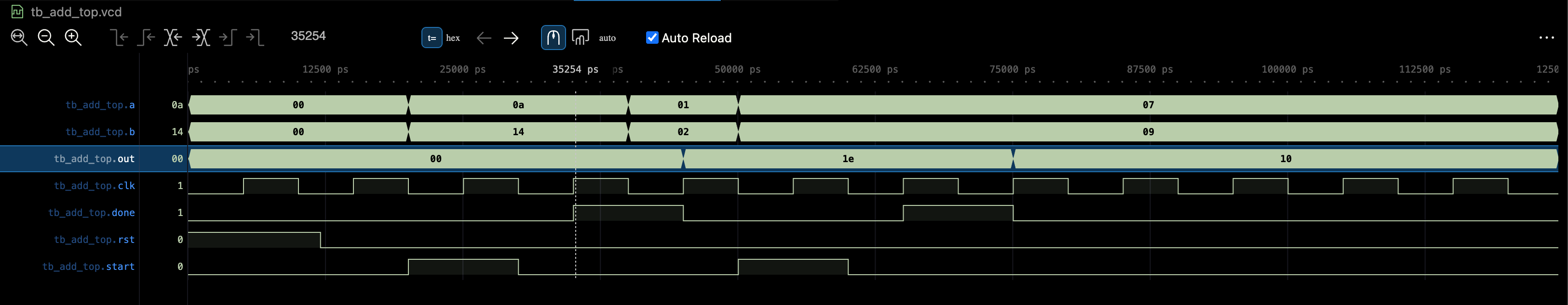
donepulses for one cycle in the write state.outupdates on theld_outcycle and then holds. The value ofoutis observed one cycle afterdone(Moore machine)- If
aandbchange after the load,outdoes not change.
This architecture with a controller and datapath follows a clear rule: the FSM emits control signals; the datapath performs computation and returns status/feedback signal. Once this rule is followed, the design becomes easier to scale to multi-step operations, waits, branches, stalls, and handshakes, with predictable simulation that matches hardware behavior. State storage for the FSM can be written inline or implemented using a DFF submodule bank. You will see the same architectural principle with Beta CPU Architecture learned in class.
Nuances
In this particular implementation (see both add_datapath and add_controller), the control signals are purely combinational from state, but state itself only changes on the clock edge. That creates a one-cycle “enable lag” relative to the edge where the state flips.
At a given posedge, every register samples its inputs using the values that were stable just before that edge. ld_out and done do not become 1 until after the edge when state has updated to S_WRITE (delta-cycle later).
So the timeline is:
- Posedge when
statebecomesS_WRITE:stateregister updates toS_WRITEat the edge.- Immediately after the edge, combinational logic makes
ld_out=1anddone=1. - But the
outregister already sampledld_outat that edge using the oldld_out(fromS_LOAD, which was 0). - Result:
donegoes high in that cycle,outdoes not update yet.
- Next posedge (when
stateleavesS_WRITEtoS_IDLE):- During the whole preceding cycle,
ld_outwas high (becausestatewasS_WRITE). - Now the
outregister samplesld_out=1at this edge and capturessum. - Result:
outupdates on this edge, which is the cycle after you first sawdonego high.
- During the whole preceding cycle,
Slowing Down an FSM for Human Observation
In an FPGA design, the system clock is usually very fast (tens of MHz). At that speed, an FSM may transition through many states in microseconds, which is far too quick to observe on LEDs or a 7-segment display. When the goal is to demonstrate behavior to a human, we do not “slow the FPGA clock down” globally. Instead, we keep the main clock unchanged and make the FSM advance only when a slower pacing signal allows it.
There are two common ways to do this. The recommended way is to use a clock-enable (tick). A less recommended way is to use a derived slow clock as an actual clock (the original Lab 4 handout in Lucid discussed about this). In this course, we emphasize the clock-enable approach because it stays within a single clock domain and avoids clocking logic with non-global clock signals.
Keep the main clock, slow the state transitions
We use slow_clock with edge_detector as input to the FSM, while still driving the FSM with the actual clk.
The key idea is to separate:
- the clock that keeps all registers synchronous (
clk) - the step condition that decides when the FSM is allowed to change state (
slow_step/slow_clock)
The FSM state register still updates on posedge clk, but it updates to the next state only on certain cycles, typically when a pulse slow_step is high. On cycles where slow_step is low, the state simply holds.
This makes the FSM appear to “run at 1 Hz” (or any human-visible rate) while still being a normal synchronous circuit under the hood.
Generating a slow pacing signal from a counter bit
A simple way to create a slow pacing signal is to increment a counter on every clock cycle and tap one of its upper bits as a slow square wave. We did it before in the previous lab:
assign slow_level = cnt[STAGES-1];
Recap on Frequency Divider Technique
Each higher bit toggles more slowly. Conceptually,
cnt[k]is a divide-by-2^(k+1)square wave. This is convenient for demonstrations because it costs almost no logic.
For your convenience, here’s a sample implementation:
module slowclock_tap_en #(
    parameter integer STAGES = 27
)(
    input  wire clk,
    input  wire rst,      // async active-high reset
    input  wire en,       // when 0: hold counter
    input  wire clr,      // async clear counter to 0
    output wire slow_clk
);

  localparam integer STAGES_I = (STAGES < 1) ? 1 : STAGES;

  reg [STAGES_I-1:0] cnt;

  always @(posedge clk or posedge rst or posedge clr) begin
    if (rst)      cnt <= {STAGES_I{1'b0}};
    else if (clr) cnt <= {STAGES_I{1'b0}};
    else if (en)  cnt <= cnt + 1'b1;
    else          cnt <= cnt; // hold
  end

  assign slow_clk = cnt[STAGES_I-1];

endmodule
However, a square wave is a level, not a step. An FSM usually needs a single-cycle “step pulse” to advance once. Therefore we typically convert slow_level into a one-cycle pulse using an edge detector.
Edge Detector
We shall turn the level square wave into a step, synchronous with the system clk. A standard approach is to detect when slow_level changes and emit a one-cycle pulse:
- rising-edge step: pulse when
slow_levelgoes0 → 1 - falling-edge step: pulse when
slow_levelgoes1 → 0 - any-edge step: pulse on either transition (twice as fast)
This is implemented by storing the previous value of slow_level in a 1-bit register and comparing current vs previous.
With our reusable register module, an edge detector is a small, modular component:
// Edge detector with selectable polarity.
// EDGE = 1 detects rising edges (0->1)
// EDGE = 0 detects falling edges (1->0)
//
// Output is a 1-cycle pulse synchronous to clk.
// Uses register.v for the 1-cycle delay storage.
module edge_detector #(
  parameter integer EDGE = 1  // 1=rising, 0=falling
)(
  input  wire clk,
  input  wire rst,
  input  wire sig,
  output wire pulse
);

  wire sig_d;

  register #(.W(1), .RESET_VALUE(1'b0)) u_dly (
    .clk(clk),
    .rst(rst),
    .en(1'b1),
    .d(sig),
    .q(sig_d)
  );

  generate
    if (EDGE) begin : G_RISE
      assign pulse = sig & ~sig_d;
    end else begin : G_FALL
      assign pulse = ~sig & sig_d;
    end
  endgenerate

endmodule
The resulting pulse is synchronous to clk and lasts exactly one clock cycle.
Using the slow step to control state transitions
There are two clean patterns. Both keep the FSM clocked by clk.
Pattern A: Gate the state register with enable
If the FSM state is stored using our register module, we can connect the step pulse to the enable:
register #(.W(STATE_W), .RESET_VALUE(S_IDLE)) u_state (
  .clk(clk),
  .rst(rst),
  .en(slow_step),     // advance only on slow_step
  .d(next_state),
  .q(state)
);
In this pattern, the combinational logic always computes next_state, but state transition is only committed when slow_step is asserted.
Pattern B: Keep enable high, but hold next_state unless stepping
Alternatively, keep the register always enabled and only change next_state on step cycles:
next_state = state;
if (slow_step) begin
  case (state)
    ...
  endcase
end
This is also correct. Pattern A is usually clearer because it highlights the idea that the slow step is a “clock-enable”.
Important timing detail: how the first step aligns
When using a tapped counter bit, the slow square wave starts from a known value after reset, typically 0. If you step only on the rising edge, the first step happens after half a slow period, but subsequent steps occur every full period. This can make the first displayed state appear shorter or longer than the others. Take a look at this waveform:
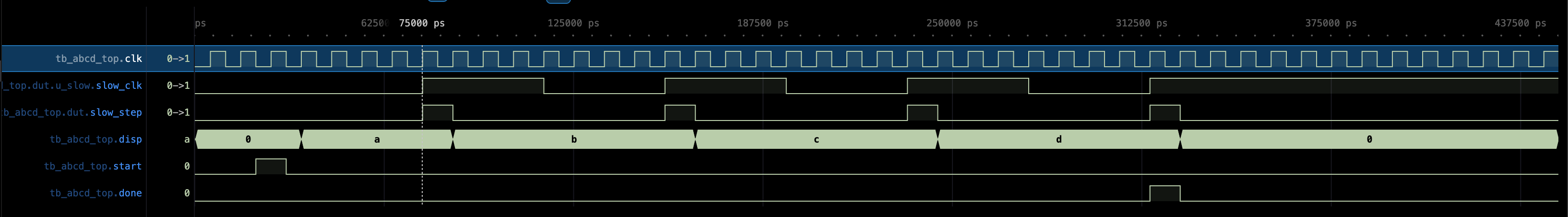
In this particular FSM example, we wanted the FSM to produce (hex) values A, B, C, then D for as long as the slow_clock period. But since slow_clock starts with 0, the slow_step signal detects the rising edge half a period later, and triggers the state transition to produce B. Afterwards, B, C, D are shown for as long as 1 full slow clock cycle.
There are three ways to address this, depending on what you want:
- Step on the falling edge instead of rising (first fall occurs after a full cycle of the slow wave).
- Step on any edge for uniform half-period steps.
When we trigger state transition on the falling edge, we can arrive in the following waveform:
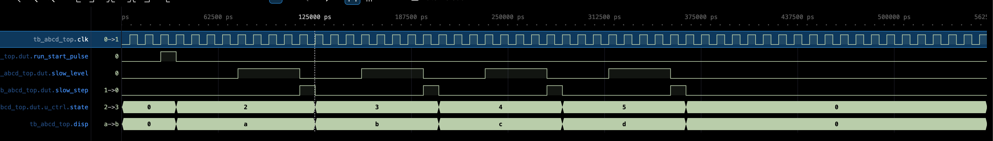
This is almost there, but notice how the device produces A for 1 clk period longer than the rest?
- This should give you a clue that it is a Moore FSM because there’s a 1 cycle lag in the state transition
- At t=115000 ps, the edge detector gives a
1as it detects the falling edge of theslow_step - This triggers the state transition, but state transition does not happen until 1
clkperiod later, resulting in “extra” clock cycle for A
If you really want to fix this, you need to add an intermediate “load” state so the start of the A sequence happens “late”. This is indicated as state 1 in the waveform below.
In practice, it wouldn’t be humanly visible to let the first state be in that state for 1 extra clk cycle because clk frequency is typically very high.
Why we do not use slow_level as an actual clock
It is tempting to write always @(posedge slow_clk) and treat the tapped bit as a real clock. On FPGA hardware, that is usually discouraged because slow_clk is not routed on the global clock network and can create clock-domain and timing problems. Using a slow_step enable keeps the entire system synchronous to the real clock and is the standard safe method.
In summary, do this to slow down an FSM for observation:
- keep the design clocked by the real
clk - generate a slow pacing signal (counter bit tap is simplest)
- edge-detect it to form a one-cycle
slow_step - advance the FSM only when
slow_stepis asserted
This keeps the RTL structurally correct (single clock domain) while producing behavior that is visible to humans on simple outputs like LEDs.
Example code
Below is a sample code you can try to implement the simple FSM that sequences through A, B, C, D slowly once start is pressed.
The controller:
module sequence_generator_controller(
  input  wire clk,
  input  wire rst,
  input  wire start,      // assumed synchronous for this example
  input  wire slow_step,  // 1-cycle pulse, synchronous to clk
  output reg  [3:0] disp,
  output reg        done
);

  localparam S_IDLE = 3'd0;
  localparam S_LOAD = 3'd1;
  localparam S_A    = 3'd2;
  localparam S_B    = 3'd3;
  localparam S_C    = 3'd4;
  localparam S_D    = 3'd5;

  wire [2:0] state;
  reg  [2:0] next_state;

  // State register uses your register.v
  register #(.W(3), .RESET_VALUE(S_IDLE)) u_state (
    .clk(clk),
    .rst(rst),
    .en(1'b1),          // state can update every clk, but next_state will hold when needed
    .d(next_state),
    .q(state)
  );

  // Next-state logic
  always @* begin
    next_state = state;

    case (state)
      S_IDLE: begin
        // if (start) next_state = S_LOAD;
        if (start) next_state = S_A;
      end

      // this state is added so that each state below has equal duration
      S_LOAD: begin
        next_state = S_A;
      end

      S_A: begin
        if (slow_step) next_state = S_B;
      end

      S_B: begin
        if (slow_step) next_state = S_C;
      end

      S_C: begin
        if (slow_step) next_state = S_D;
      end

      S_D: begin
        if (slow_step) next_state = S_IDLE;
      end

      default: begin
        next_state = S_IDLE;
      end
    endcase
  end

  // Output decode
  // Moore FSM
  always @* begin
    disp = 4'h0;
    case (state)
      S_A: disp = 4'hA;
      S_B: disp = 4'hB;
      S_C: disp = 4'hC;
      S_D: disp = 4'hD;
      default: disp = 4'h0;
    endcase
  end

  // done pulses when we are in D and a slow_step occurs (D -> IDLE transition)
  always @* begin
    done = (state == S_D) & slow_step;
  end

endmodule
Top module:
module sequence_generator_top #(
  parameter integer STAGES = 5
)(
  input  wire clk,
  input  wire rst,
  input  wire start,
  output wire [3:0] disp,
  output wire done
);

  // running flag: set by start, cleared by done
  wire running;
  wire running_d;

  assign running_d = (running | start) & ~done;

  register #(.W(1), .RESET_VALUE(1'b0)) u_running (
    .clk(clk),
    .rst(rst),
    .en(1'b1),
    .d(running_d),
    .q(running)
  );

  // clear slow counter exactly when a new run starts (rising edge of running)
  wire run_start_pulse;
  edge_detector #(.EDGE(1)) u_run_start (
    .clk(clk),
    .rst(rst),
    .sig(running),
    .pulse(run_start_pulse)
  );

  // slow square wave only runs while running=1
  wire slow_level;
  slowclock_tap_en #(.STAGES(STAGES)) u_slow (
    .clk(clk),
    .rst(rst),
    .en(running),
    .clr(run_start_pulse),
    .slow_clk(slow_level)
  );

  wire slow_step;

  // detect on FALLING edge
  // slow clock produces LOW then HIGH. without inverting, we will end up with S_A being shown for half a slow_clock + 1 clk cycle
  // this ensures that S_A is shown for 1 full slow clock cycle
  edge_detector #(.EDGE(0)) u_step (.clk(clk), .rst(rst), .sig(slow_level), .pulse(slow_step));

  sequence_generator_controller u_ctrl (
    .clk(clk),
    .rst(rst),
    .start(run_start_pulse),
    .slow_step(slow_step),
    .disp(disp),
    .done(done)
  );

endmodule
And the corresponding tb. Note that we just set STAGES as 3 to demonstrate the idea. If clk is 100MHz like your Alchitry Au Board, then you should set STAGES as 27 or 28 for a comfortable rate (about once per second).
`timescale 1ns/1ps

module tb_abcd_top;

  reg clk, rst, start;
  wire [3:0] disp;
  wire done;

  sequence_generator_top #(.STAGES(3)) dut (
    .clk(clk),
    .rst(rst),
    .start(start),
    .disp(disp),
    .done(done)
  );

  initial begin
    clk = 1'b0;
    forever #5 clk = ~clk; // 10 ns period
  end

  initial begin
    $dumpfile("tb_sequence_generator_top.vcd");
    $dumpvars(0, tb_abcd_top);

    rst = 1'b1;
    start = 1'b0;

    #20 rst = 1'b0;

    // start pulse can be short because IDLE checks start every normal clk
    @(negedge clk);
    start = 1'b1;
    @(negedge clk);
    start = 1'b0;

    // wait until sequence completes
    @(posedge done);

    // let it sit in IDLE for a bit
    #200;

    $finish;
  end

endmodule
Run on FPGA
This section describes the hardware toolchain required to run your design on a real FPGA (the Alchitry Au board lent to your group). At this stage, you are no longer simulating logic behavior and you are converting synthesizable Verilog into a physical configuration bitstream that programs the FPGA fabric.
Toolchain Overview
-
Icarus Verilog: Used for simulation only. It parses Verilog, elaborates the design, and evaluates behavior over time. It does not perform synthesis, place-and-route, or bitstream generation.
- Vivado: Xilinx’s FPGA implementation toolchain. It performs:
- RTL synthesis into logic primitives
- Technology mapping for the Artix-7 FPGA on the Alchitry Au
- Place and route
- Bitstream generation (Only tools like Vivado can produce a
.binfile that configures an FPGA)
- Alchitry Labs V2: A project manager and frontend that integrates with Vivado. It handles pin constraints, board definitions, IO shields, and loading the final bitstream onto the FPGA.
Because of this division of responsibility, Icarus Verilog cannot be used to run designs on FPGA hardware. It has no knowledge of FPGA architecture and no ability to generate configuration data.
Install Vivado
You need Vivado toolchain to generate the bitstream for the Alchitry Au FPGA. Consult the installation page.
Create a New Project on Alchitry Labs V2
Download Alchitry Labs V2 if you haven’t already. Set Vivado’s path to point to the Vivado folder you just installed. Then, create a new io project on Alchitry Labs with Io V1 Base Pulldowns as the template:
Afterwards, import all your Verilog files to the project. You should see them in the source file once you have migrated all of them over.
Finally, you need to connect your verilog top module into alchitry_top. This is one example:
module alchitry_top (
    input clk,              // 100MHz clock
    input rst_n,            // reset button (active low)
    output led[8],          // 8 user controllable LEDs
    input usb_rx,           // USB->Serial input
    output usb_tx,          // USB->Serial output
    output io_led[3][8],    // LEDs on IO Shield
    output io_segment[8],   // 7-segment LEDs on IO Shield
    output io_select[4],    // Digit select on IO Shield
    input io_button[5],     // 5 buttons on IO Shield
    input io_dip[3][8]      // DIP switches on IO Shield
) {

    sig rst                 // reset signal
    .clk(clk) {
        // The reset conditioner is used to synchronize the reset signal to the FPGA
        // clock. This ensures the entire FPGA comes out of reset at the same time.
        reset_conditioner reset_cond
        button_conditioner conditioner(#CLK_FREQ(100000000),.in(io_button[0])) // start button

    }

    sequence_generator_top device(#STAGES(27), .clk(clk), .rst(rst), .start(conditioner.out))

    always {
        reset_cond.in = ~rst_n  // input raw inverted reset signal
        rst = reset_cond.out    // conditioned reset

        led = 8h00              // turn LEDs off

        usb_tx = usb_rx         // loop serial port

        io_led = {8h00, 8h00, c{4h0, device.disp}} // use io_led[0] for display
        io_segment = 8hff
        io_select = 4hf
    }
}
Note that you cannot rely on Alchitry’s simulator. It is not designed to simulate Verilog modules.
You can click build, and once the build is successful, switch to Alchitry Loader:
Finally, connect your FPGA and load the binary. If you load the sample code above, you should see the io_led blinking slowly as start button (io_button[0]) is pressed.
While you technically can skip Alchitry Labs entirely and use Vivado directly to generate the bitstream, the steps are more involved. You can refer to [this]() guide instead.
Processing Button Presses
To simplify things, you are recommended to pass the conditioned button presses (so it’s sync to clk and debounced) before passing the level signal to your Verilog top.
You will need to create a button conditioner to process the button presses. You can do this easily in Lucid, inside alchitry_top, then pass your conditioned button presses (level wave) into your top Verilog module. Read the Lucid lab handout for details.
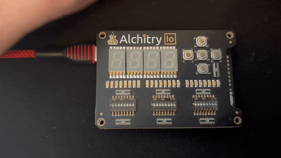
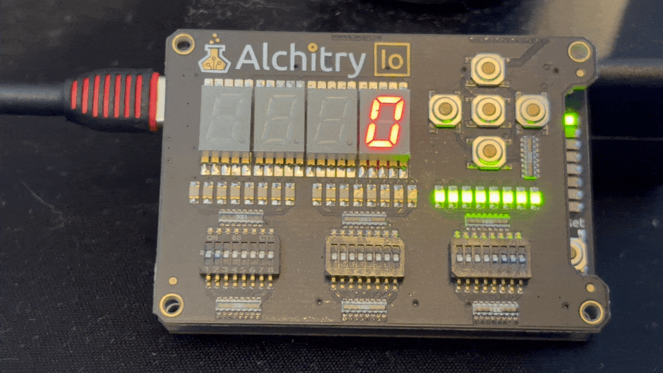
Build Automated Register Adder Tester
Suggested design
You are to test the functionality of your REGISTERED 8-bit RCA (registers a, b, and s are required!) automatically here by using an fsm. You may choose to use write-enabled register or not. Your implementation should adapt accordingly.
Similar to the previous lab, you can create constants that stores the following:
A_INPUTS[i]: the i-th test value for operanda.B_INPUTS[i]: the i-th test value for operandb.SUMS[i]: the expected sumA_INPUTS[i] + B_INPUTS[i].index: a DFF that stores which test case we are currently applying.
If you have N test cases, then A_INPUTS, B_INPUTS, and SUMS are all N by 8 array. index has the size of log2(N) bits.
On each slow clock tick (for example near 1 Hz):
indexincrements by 1 (wrapping around at the end).- The current
aandbinputs toregistered_rca_enare taken fromA_INPUTS[index.q]andB_INPUTS[index.q]. - The adder computes
s. - Hardware compares
swith pipelinedSUMS[index.q]. - The LEDs display
a,b,s, and an error flag.
Alchitry Simulator doesn’t work with Verilog
There’s no way to test that your code is working using Alchitry Simulator. You would need to build and load to FPGA to test whether it works on hardware.
Here’s an example demo:
Summary
In this lab you implement a controller–datapath system in Verilog:
- an FSM (controller) generates control signals to sequence multi-step behavior,
- a datapath containing the registers, MUXes, and arithmetic, and returns simple status signals for the FSM to react to
You practice writing structurally clean RTL by keeping state updates clocked (nonblocking) and keeping control decode combinational with explicit defaults, then verify the timing you observe in simulation (including the common one-cycle Moore-style “enable/output lag”).
You also learn a safe way to make an FSM human-observable on FPGA: by keeping the real clock, but advance state only on a slow step pulse derived from a counter bit plus an edge detector (clock-enable style, single clock domain).
Finally, you run the design on hardware by building a bitstream with Vivado through Alchitry Labs/Loader, and apply the same approach to build an automated registered adder tester driven by an FSM, with button conditioning handled in Lucid at the top level.