 50.002 CS
50.002 Computation Structures
Information Systems Technology and Design
Singapore University of Technology and Design
Driving MAX7219 with an FPGA
Driver Code
You can download the driver code from here. They are designed to work together.
The entire repository with demo code can be found here.
Overview
The MAX7219 is a general-purpose LED display driver that can control either up to 8 digits of 7-segment LEDs or an 8×8 LED dot matrix. In both cases, the FPGA communicates with the MAX7219 using the same 3-wire serial interface (DIN, CLK, CS) to send configuration commands and display data. This driver implements the MAX7219 command framing and initialization sequence, so your top-level design only needs to provide the values/patterns to be displayed.
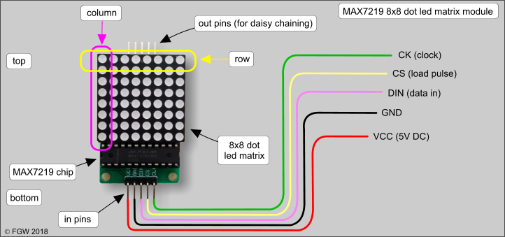
Image taken from here.
Whether the module is 7-segment or dot-matrix mainly changes how you interpret the 8 data registers (digits vs rows); the serial protocol is unchanged.
If you use it to drive 8 digits of 7-segment, this is what you have:
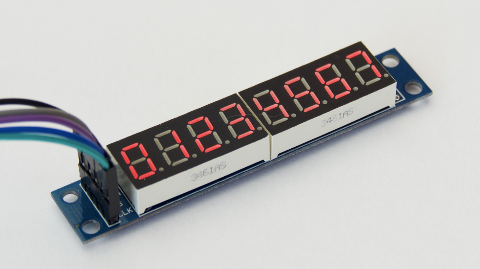
You can likewise use it to drive 8x8LED dot matrix, one row corresponds to each “digit” in the segment.
How MAX7219 Works
The MAX7219/MAX7221 is a serially interfaced LED driver for common-cathode displays. It can drive up to 8 digits of 7-segment LEDs, bar graphs, or a 64-LED (8×8) matrix, and it handles multiplex scanning plus segment current control internally.
If you want to connect multiple 8x8 matrices, then you need to daisy-chain several MAX7219/7221 chips. You can change the
CHAINparameter in the demo code to test that.
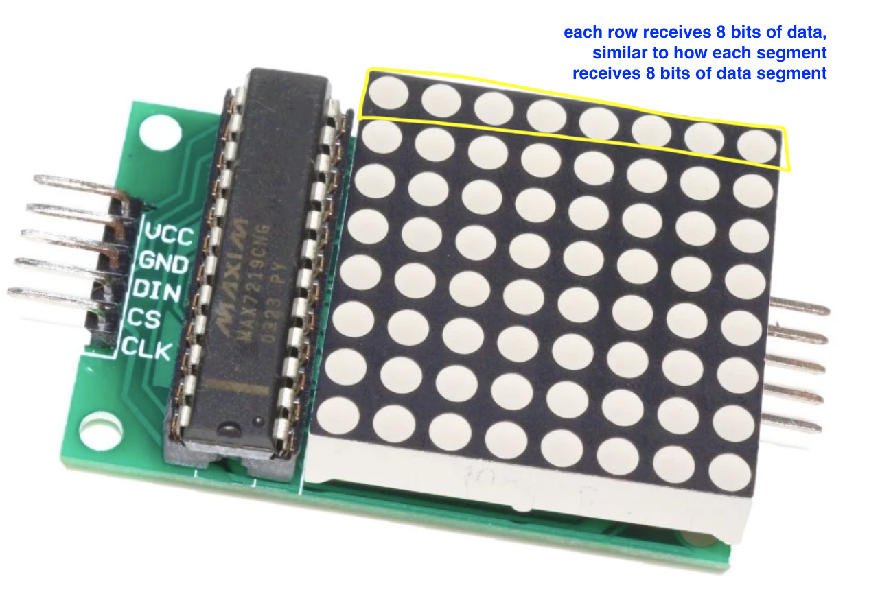
You would typically already buy a MAX7219 connected to a series of 7-segment or dotmatrix as shown in the figure on the right. MAX7219 chip itself has many output connections shown in the figure on the left.
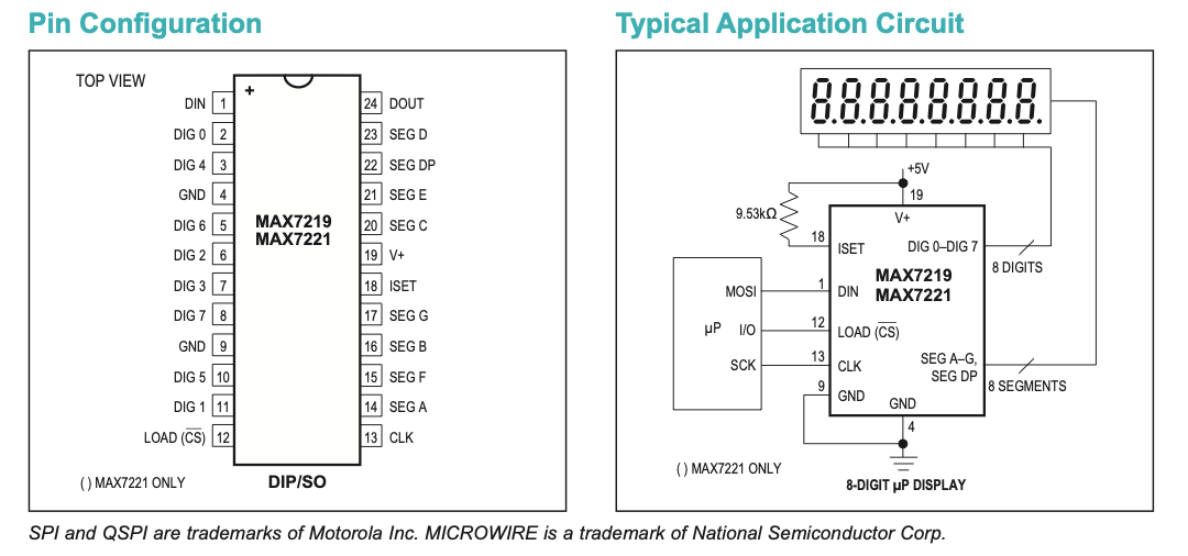
The FPGA talks to it over DIN, CLK, and LOAD/CS. Data is sent as 16-bit frames and latched on the rising edge of LOAD/CS after the 16th clock and stores it in the internal registers inside MAX7219.
Frame layout: bits sent by the FPGA are D0–D15. D8–D11 are the register address, D0–D7 are the data, and D12–D15 are don’t-care. The first bit sent is D15 (MSB first).
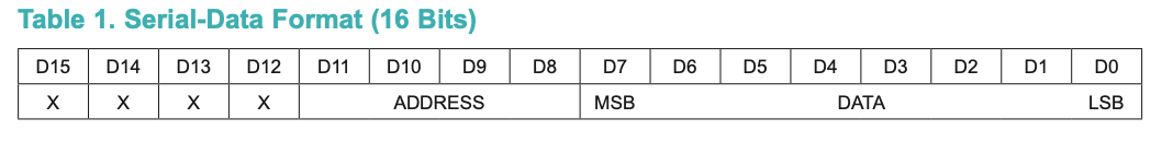
The register address is in bits D8–D11 and the data is in bits D0–D7 (D12–D15 are don’t care). These registers hold values for each segment value up to 8 digits (or 8 rows of the matrix) and are meant to drive these digits at all times.

In the serial module (max7219_serial.luc), start=1 triggers one transaction:
- pull cs/load low (device listens)
- shift 8 address bits, then 8 data bits (total 16 clocks)
- pulse cs/load high to latch the packet
- return to
IDLE(busy=0) so the driver can send the next packet
Internally, the digit/row values are stored in an on-chip 8×8 RAM, so you can update one digit (or one row) without rewriting everything.
On power-up, the display is blanked and the chip starts in shutdown mode, so you must configure key control registers (decode mode, scan limit, intensity) and then exit shutdown before displaying.
The driver module contains an FSM that does the following:
Blank it while configuring
SEND_INITIAL_SHUTDOWN
- Write Shutdown register (0x0C) = 0 (shutdown mode, display blank but registers keep their values).
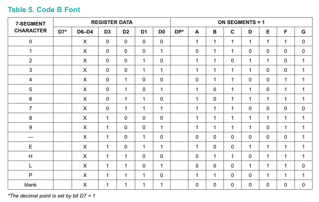
Choose how digit data is interpreted
SEND_NO_DECODE
-
Write Decode Mode register (0x09) = 0x00 (no-decode for all digits, so D7–D0 map directly to segments/LED lines).
-
If you were doing 7-seg with Code-B decoding (automatically write chars 0-9 without individual segments), you would set bits in 0x09 instead, but this driver assumes raw segment/row control.
Enable all 8 digits/rows
SEND_SCAN_ALL_DIGITS
- Write Scan Limit register (0x0B) = 0x07 to scan/display digits 0–7 (8 total).
Write the display RAM (the actual pixels/segments)
SEND_WORD (repeats 8 times)
-
For digit_index = 0..7, write one digit register:
- Address = Digit 0..7 registers (0x01..0x08) from the register map
- Data = your
segment_values[digit_index](one byte per digit/row, already bit-reversed in your assumption)
This matches the datasheet note that digit registers are implemented as an on-chip 8×8 SRAM, so you update one “row/digit” at a time.
Turn scanning back on so it becomes visible
SEND_TURN_ON
- Write Shutdown register (0x0C) = 1 for normal operation.
What happens on each update (new)
In the serial module, when new=1 in IDLE, we do SEND_SHUTDOWN to SEND_WORD (8 writes) to SEND_TURN_ON.
That is a clean “blank while updating” pattern using shutdown, and it is consistent with the datasheet description of shutdown blanking while keeping register contents.
Intensity and display-test fit (optional)
Intensity register = 0x0A, and the lower nibble controls brightness in 16 steps. You can send this once during init (typically after scan-limit, before turning on).
Display Test register = 0x0F forces all LEDs on (and stays that way until you clear it). The driver FSM includes a test-on and test-off path, which is exactly the intended usage. You should omit this state during production.
CHAIN behavior
For chaining, DOUT allows multiple MAX7219s to be daisy-chained.
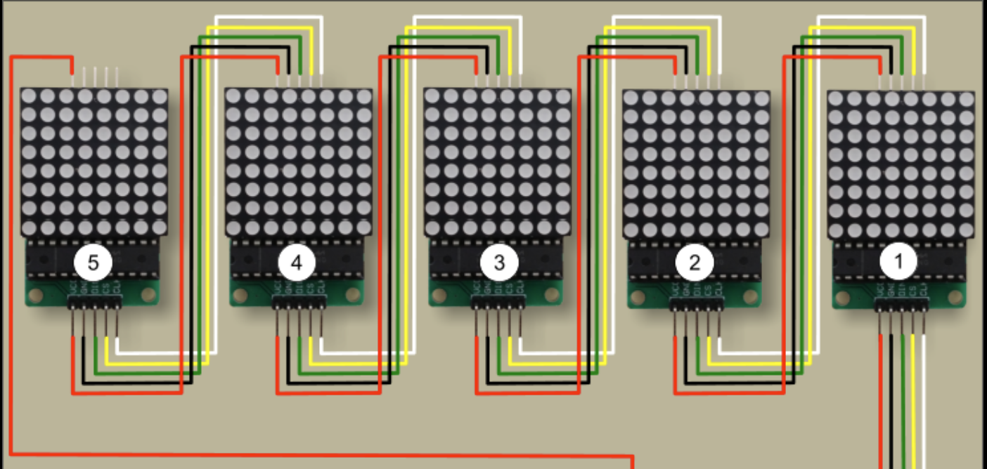
Image taken from here.
Daisy chaining is supported via DOUT, and DIN data appears at DOUT 16.5 clocks later, enabling cascades.
For CHAIN = N, you must shift N packets (N×16 bits) before pulsing LOAD/CS once, so all devices latch simultaneously (addr_in[8*CHAIN] and din[8*CHAIN] exist to carry N address bytes and N data bytes per transaction).
If you ever want to target only one chip in a chain, the datasheet’s mechanism is NO-OP (address 0x00) for the other chips while shifting the real command for the target chip.