 50.002 CS
50.002 Computation Structures
Information Systems Technology and Design
Singapore University of Technology and Design
Generating New Clock Frequencies
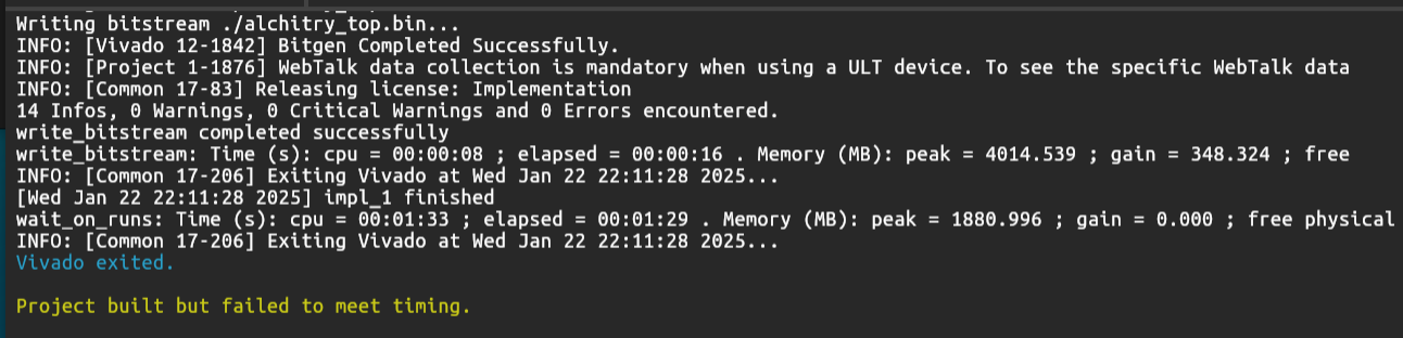
This document is written to guide you with generating new clock signals for your project should it fails to meet timing specifications. If your project works in simulation but behaves erratically on physical FPGA, it is likely that you have timing issues.
Motivation
The Alchitry Au FPGA board runs at a default system clock of 100 MHz, which is generated by an onboard oscillator. It is a crystal oscillator module soldered onto the board that provides a clean 100 MHz square wave clock signal. However, sometimes your design might fail to meet the timing constraints, e.g: ALU multiply takes too long and violates the t2 constraint:
To make your project works reliably, you need to add extra logic to slow your FSM (let it loop for several cycles before capturing its result) or to slow down the clock. The latter is more straightforward but cumbersome to do: it requires you to access Vivado and generate clock with another frequency.
Changing the clock frequency in the alchitry.acf constraint file does not change the default clk signal going to your alchitry_top. The constraint file is for telling the tools what the frequency is for timing analysis only, not to control the frequency.
Method 1: Delay the FSM
If you need more than 10 ns (since the onboard clock is fixed at 100Mhz) of time per state, for instance: your ALU’s tpd for CMPEQ or MUL is taking too long, you need to loop a few times in the same state before capturing the output of your ALU. Otherwise, your ALU won’t be able to output the correct value in the same clock cycle.
The following state won’t behave as expected. We won’t store the right CMPEQ result into R6 in this state for example:
    States.CHECK_SCORE:
        alufn = b110011 // CMPEQ
        regfile_ra1 = d1 // score dff
        asel = b00 // rd1 to alu
        bsel = b01  // constant 10
        regfile_we = 1
        regfile_wa = d6 // temp dff
        game_fsm.d = States.BRANCH_SCORE
You should have fixed your ALU to be able to output a stable result within 1 period of FSM clock (remove any sequential component). However, if you need to have any sequential (like division) or complex component (very long tpd) in the ALU, then you will need to wait several cycles in this state before advancing to the next state, e.g BRANCH_SCORE.
You can do this by declaring a temp dff in your control unit / fsm module:
dff state_delay[4](.clk(clk), .rst(rst), #INIT(0))
And then utilise this in the state to introduce delay:
    States.CHECK_SCORE:
        // increment state_delay
        state_delay.d = state_delay.q + 1
        alufn = b110011 // CMPEQ
        regfile_ra1 = d1 // score dff
        asel = b00 // rd1 to alu
        bsel = b01  // constant 10
        regfile_wa = d6 // temp dff

        if (&state_delay.q){
            regfile_we = 1  // write only once at the end of the delay cycle
            state_delay.d = 0 // reset state_delay
            game_fsm.d = States.BRANCH_SCORE // go to next state
        }
This way, the FSM maintains the same control signal for 16 onboard clock cycles (160ns) and then only capture the output at the the 16th cycle, while transitioning to the next state. This should give enough time for the ALU output to settle. You should adjust the size of the dff accordingly.
You can find out how long you need to wait for the output of the ALU to stabilize by changing the clock frequency in alchitry.acf file.
Method 2: Generate New Clock Signal using Clock Wiz in Vivado IP Catalog
In this method, we will use Vivado to use a MMCM (Mixed-Mode Clock Manager) to generate a custom clock signal from the default 100 MHz input clock.
MMCM
An MMCM (Mixed-Mode Clock Manager) is a clock management block in Xilinx FPGAs that generates derived clocks with configurable frequency, phase, and duty cycle.
Open Vivado IP Catalog from the component menu:
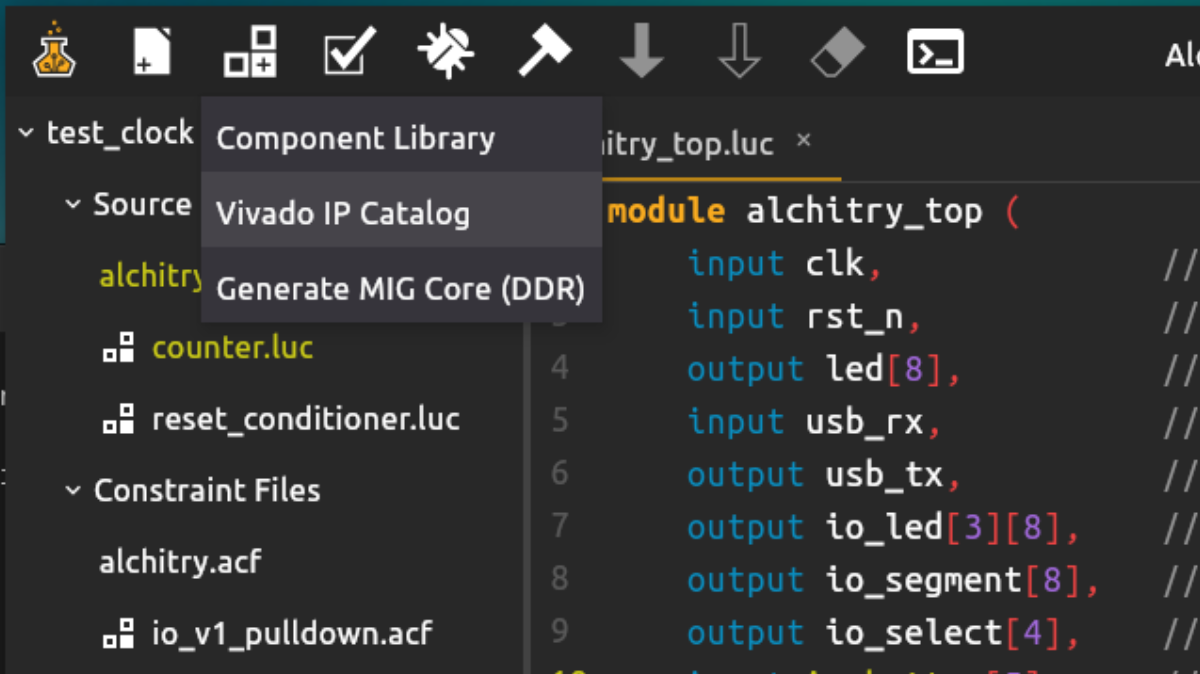
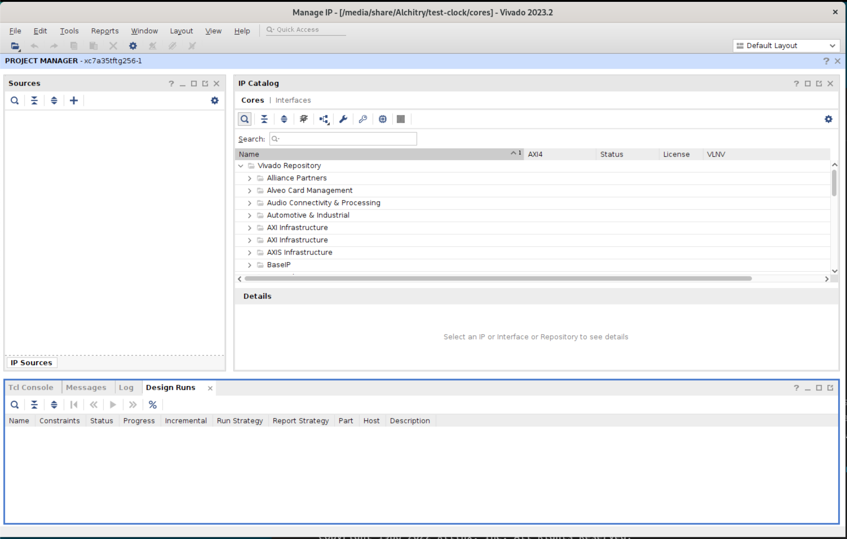
Wait awhile, and you will see Vivado launched:
Search Clocking, then double click Clocking Wizard to launch:

The Clocking Wizard window will appear. At the Clocking Options tab, choose MMCM. The MMCM module will be expecting a 100MHz input signal, and is coming from the Single-ended clock capable pin, N14, from your Alchitry Au.
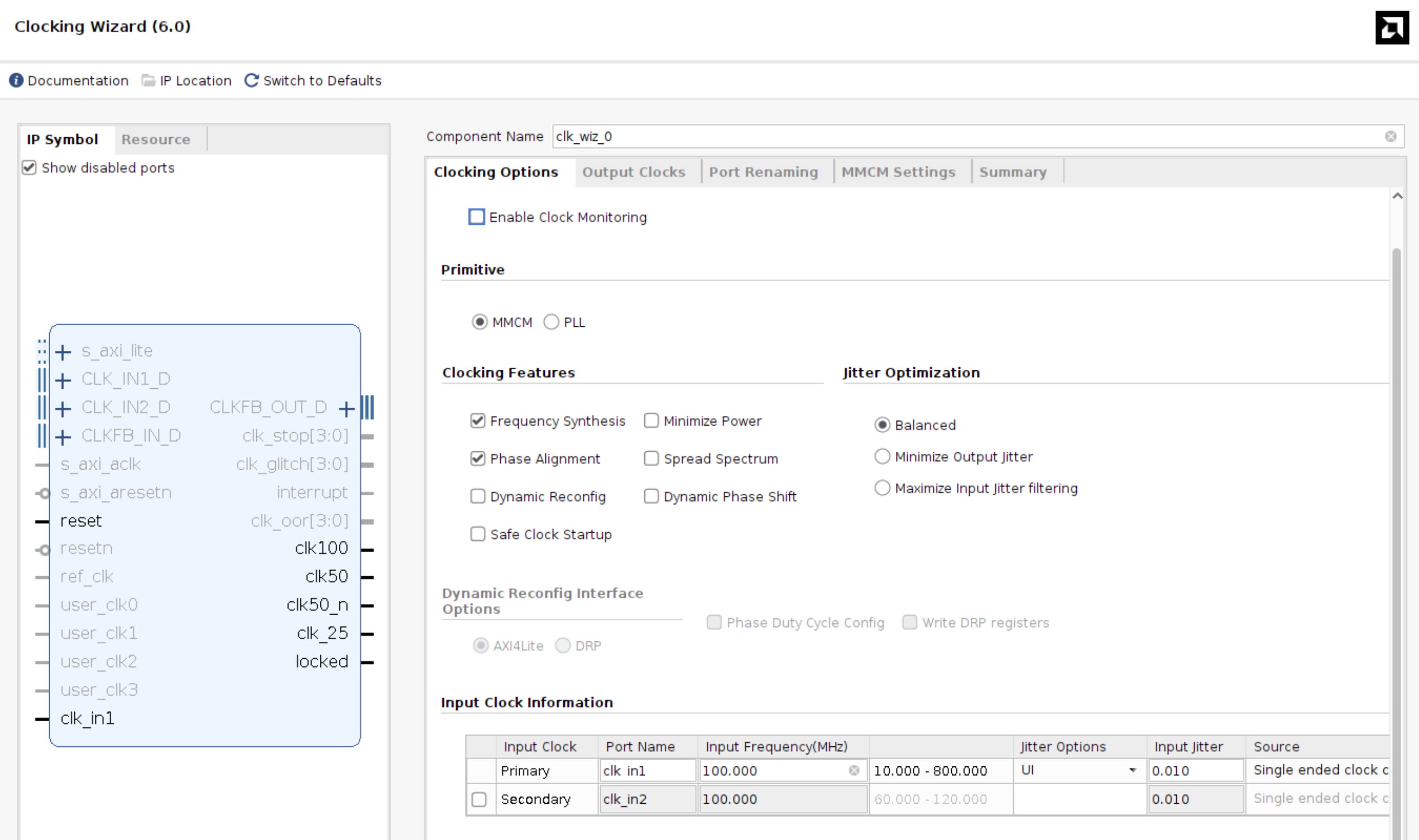
Then, at the Output Clocks tab, change the Requested Frequency to be the one you want, e.g: 10MHz. You might also want to change the output port name to follow the frequency so you remember which port is producing which frequency.
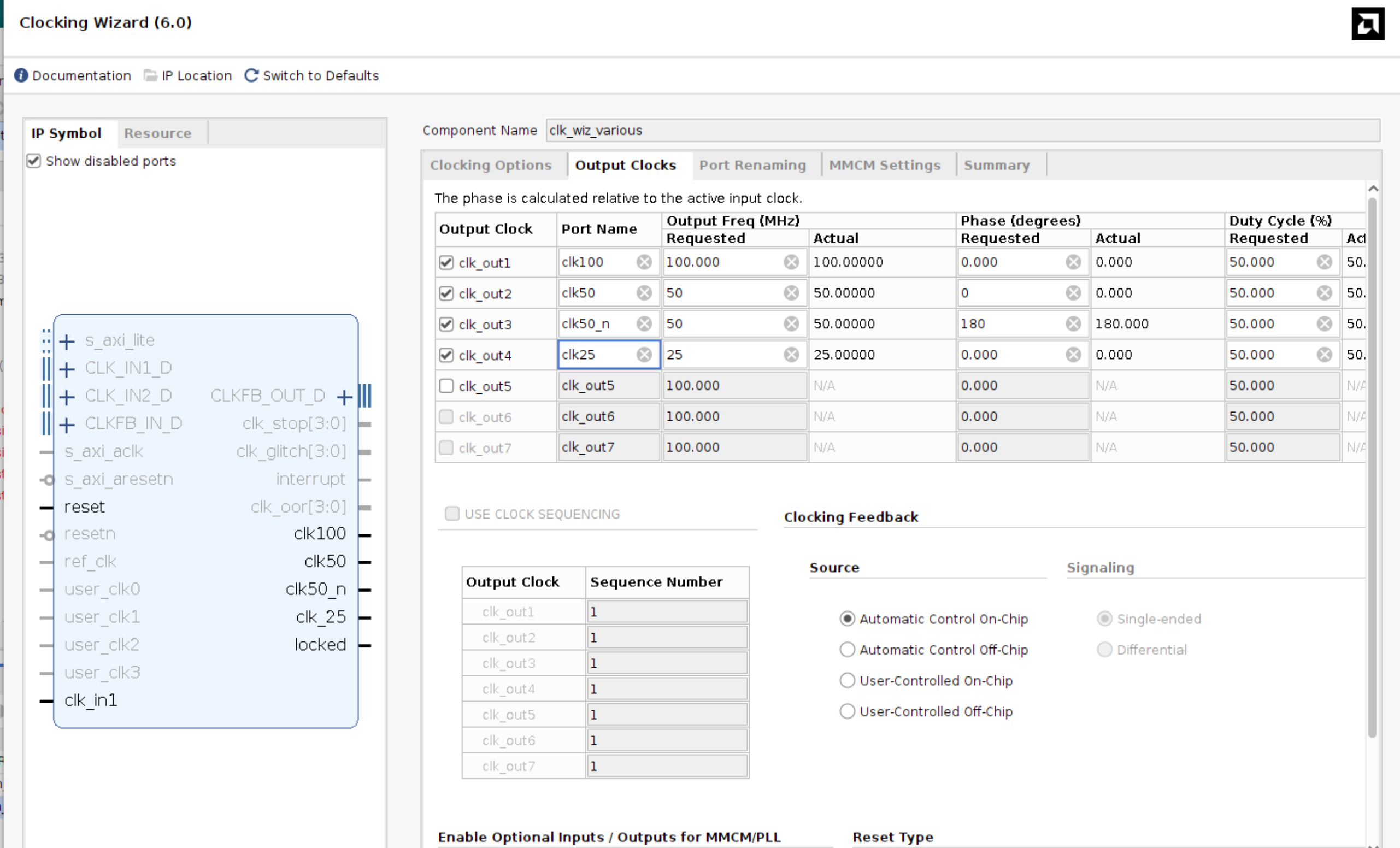
Phase Setting
For phase, it sets far you shift a clock waveform relative to its “normal” starting position, measured in degrees out of 360. 360 degrees means one full period of that clock. For example, for a 50MHz clock (20ns period)
- Rising edges at: 0, 20, 40, 60, 80 ns…
- Falling edges at: 10, 30, 50, 70, 90 ns…
If we apply a 180 degree phase shift, we can compute phase shift in time = (180 / 360) x 20 ns = 0.5 x 20 ns = 10 ns
So every edge shifts forward by 10 ns:
- Rising edges at: 0+10, 20+10, 40+10… = 10, 30, 50, 70, 90 ns…
- Falling edges at: 10+10, 30+10, 50+10… = 20, 40, 60, 80, 100 ns…
You can apply phase shift as necessary to align rising/falling edges of various clock signals you are generating.
Gating reset on locked
locked is an output signal from the clock_wiz IP that goes HIGH when the MMCM has stabilized and its output clocks are reliable.
When the FPGA first powers up or comes out of reset, the MMCM needs some time to lock onto the input clock and settle its VCO and dividers. During this startup period, the output clocks are not yet stable. locked stays LOW during this time and only goes HIGH once the MMCM is confident its outputs are correct.
Therefore, you shall use it to hold your entire design in reset until it is safe to run:
    sig rst                 // reset signal
    clk_wiz_various clocks(.clk_in1(clk), .reset(~rst_n))

always{
    reset_cond.in = ~rst_n | ~clocks.locked
}
This means your design stays in reset if either the user pressed reset, or the MMCM has not locked yet. Without this, your flip flops could start clocking on garbage clock signals during MMCM startup and end up in an undefined state even after locked goes high.
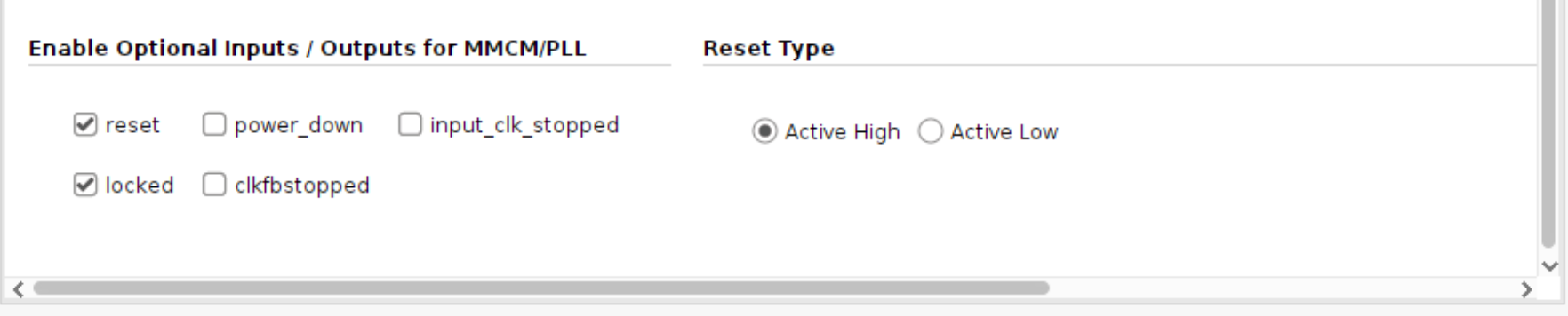
Feed raw rst_n
Do not pass the output of reset_conditioner into reset port of the clk_wiz_* module. This is because Clocking Wizard reset asynchronously clears the MMCM/PLL internal state and restarts lock when released. Instead, pass rst_n directly from alchitry_top board:
clk_wiz_various clocks(.clk_in1(clk), .reset(~rst_n))
AMD also documents that the wizard reset type is configurable, with active-high as the default.
Generate
Finally, click OK then Generate:
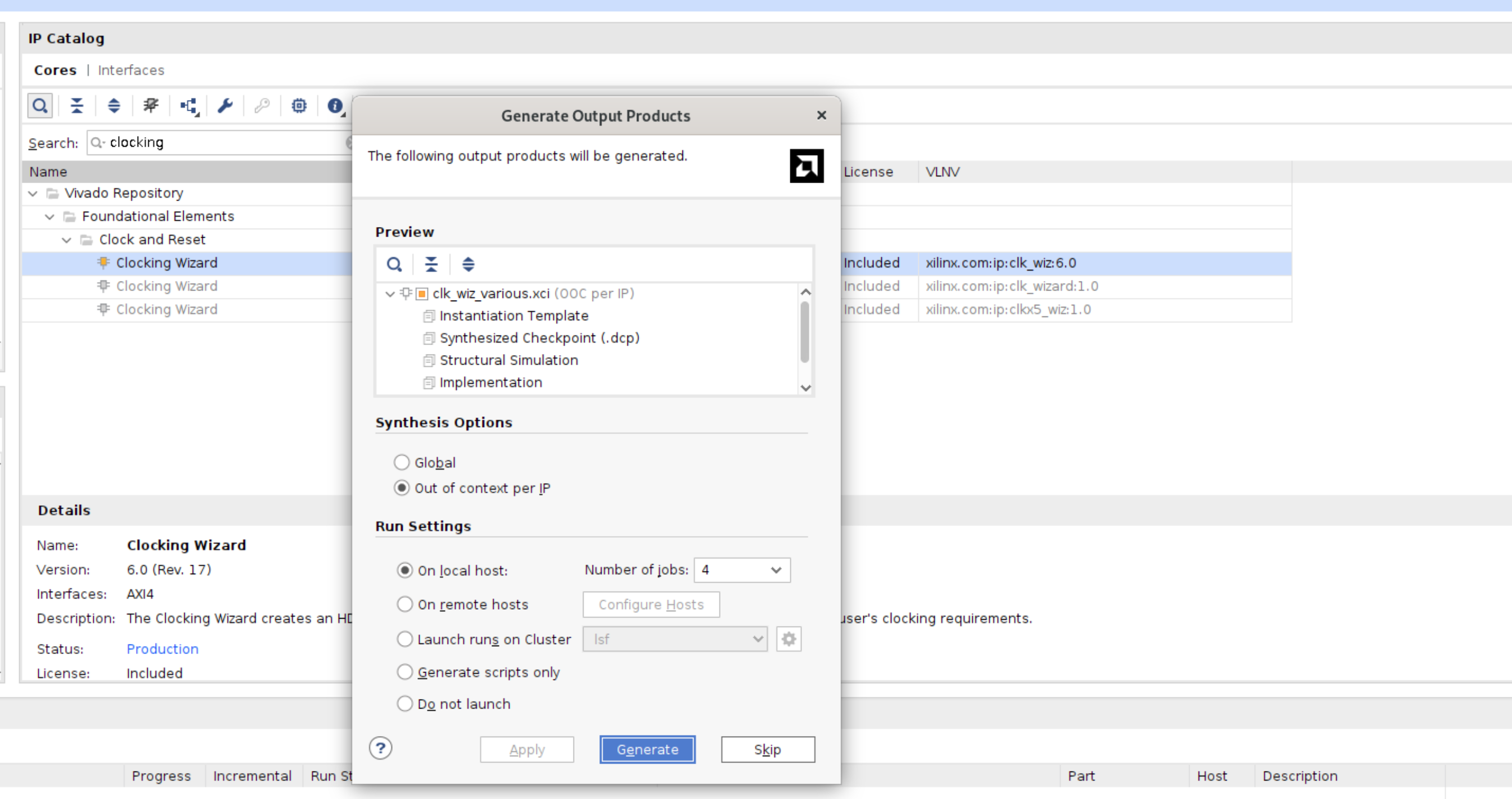
It will take some time. Get some coffee and return later.
Once done, you can close Vivado. When you return to Alchitry Labs, you will see your new clock created:
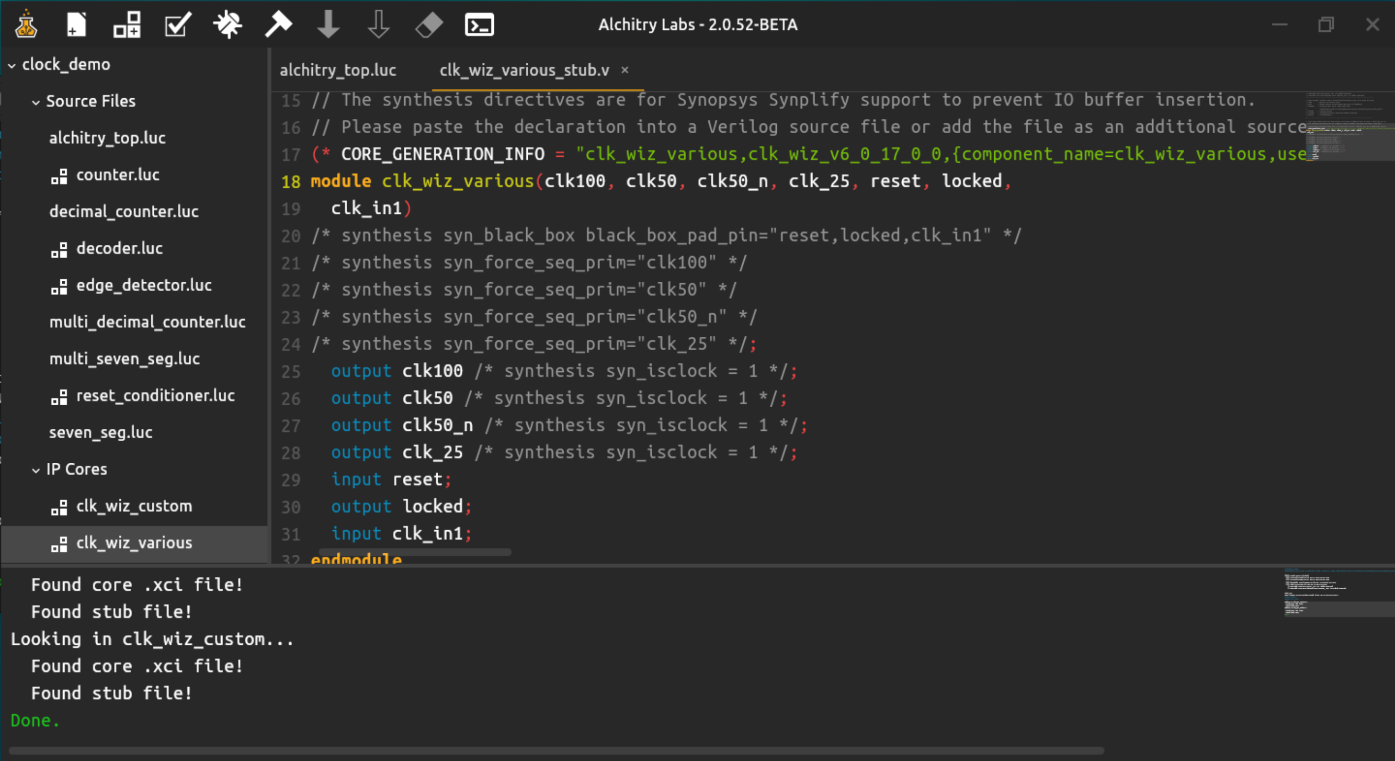
You can then use it like any other module:
    clk_wiz_various clocks(.clk_in1(clk), .reset(rst))

    .clk(clocks.clk25){
        dff slow_counter[32](.rst(rst))
    }
The Original 100Mhz clock
Once you feed the raw onboard clock into clk_wiz, do not use it anywhere else. The MMCM inside clk_wiz introduces phase shifts on all its outputs, so mixing the raw input with any clk_wiz output gives you unknown phase relationships between clock domains, causing metastability.
Instead, configure clk_wiz to output all the frequencies you need, including 100 MHz, and use only those outputs downstream. Here’s one example:
All outputs from the same clk_wiz instance have a known phase relationship since they come from the same MMCM. Also gate your reset on locked so your design stays in reset until the MMCM stabilizes.
Test
Create a regular io_demo V1 with pulldown starter project on Alchitry Labs. Then after creating the clocks as per the screenshot, test them this way. This alchitry_top.luc file blinks two LEDs (led[1:0]) while doing the regular io_demo sequence:
module alchitry_top (
    input clk,              // 100MHz clock
    input rst_n,            // reset button (active low)
    output led[8],          // 8 user controllable LEDs
    input usb_rx,           // USB->Serial input
    output usb_tx,          // USB->Serial output
    output io_led[3][8],    // LEDs on IO Shield
    output io_segment[8],   // 7-segment LEDs on IO Shield
    output io_select[4],    // Digit select on IO Shield
    input io_button[5],     // 5 buttons on IO Shield
    input io_dip[3][8]      // DIP switches on IO Shield
) {

    sig rst                 // reset signal
    clk_wiz_various clocks(.clk_in1(clk), .reset(~rst_n))
    .clk(clocks.clk100) {
        // The reset conditioner is used to synchronize the reset signal to the FPGA
        // clock. This ensures the entire FPGA comes out of reset at the same time.
        reset_conditioner reset_cond

        edge_detector edge_detector(#RISE(1), #FALL(0))

        .rst(rst) {
            // Reduce DIV values for simulation so it doesn't take forever
            multi_seven_seg seg (#DIV($is_sim() ? 1 : 16), #DIGITS(4))
            multi_decimal_counter dec_ctr (#DIGITS(4))
            counter ctr (#SIZE(1), #DIV($is_sim() ? 8 : 24))
        }
    }

    always {
        reset_cond.in = ~rst_n | ~clocks.locked  // input raw inverted reset signal
        rst = reset_cond.out    // conditioned reset

        led = c{3b0, io_button} // connect buttons to LEDs

        usb_tx = usb_rx         // loop serial port

        edge_detector.in = ctr.value
        dec_ctr.inc = edge_detector.out
        seg.values = dec_ctr.digits

        io_segment = ~seg.seg // connect segments to the driver
        io_select = ~seg.sel  // connect digit select to the driver

        io_led = io_dip       // connect the DIP switches to the LEDs
        led[0] = clocks.clk100
        led[1] = clocks.clk50
        led[2] = clocks.clk_25
        led[3] = clocks.locked
        led[4] = ctr.value

    }
}
You can refer to this repository for the source code and build for this simple clock demo.
Summary
If your project works in simulation but behaves erratically on physical FPGA, it is likely that you have timing issues.
Whenever your project fails to meet timing constraints, remember to:
- Modify
alchitry.acfto let Vivado do the timing analysis properly with the new clock frequency and ensure that it meets the timing constraints - Create a new clock using Vivado Clock Wiz (better choice), or manually delay certain FSM states where you suspect takes more than 10ns to complete (works, but more of a guessing game)