 50.002 CS
- Overview
- N-input Gates
- Sum of Products
- Straightforward Logic Synthesis
- Boolean Algebra Properties
- Universal Gates
- Special Combinational Logic Devices
- Summary
- Appendix
50.002 Computation Structures
Information Systems Technology and Design
Singapore University of Technology and Design
Logic Synthesis
You can find the lecture video here. You can also click on each header to bring you to the section of the video covering the subtopic.
Detailed Learning Objectives
- Explain the Basics of Logic Synthesis:
- Explain how combinational logic devices synthesize logic to produce specific outputs based on given inputs, adhering to functional specifications or truth tables.
- Explain how functional specifications are expressed through truth tables for different logic gates like NAND and AND.
- Explain Multi-input Logic Gates:
- Explain the concept of multi-input gates and recognize the computational possibilities and limitations of different gate types.
- Justify how the number of possible logic gates increases exponentially with the number of inputs.
- Apply Sum of Products Method (SoP):
- Compute Boolean expressions from given truth tables using the sum of products method.
- Explain the process of creating combinational logic expressions that align with specified truth tables using SoP.
- Synthesize Logic Using Basic Logic Gates:
- Syntheize any given Boolean expression with the use of basic logic gates (INV, AND, OR, XOR).
- Apply straightforward logic synthesis to build complex combinational devices from basic components.
- Utilize Boolean Algebra for Logic Minimization:
- Apply Boolean algebra properties to manipulate and simplify Boolean expressions.
- Identify various Boolean algebra rules and their applications in reducing logic complexity.
- Explain Universal Gates:
- Explain how NAND and NOR gates as considered as universal gates capable of implementing any Boolean function.
- Practice how to construct basic logic functions using only NAND or NOR gates.
- Identify Special Combinational Logic Devices:
- Examine the functionality and application of multiplexers and demultiplexers in digital circuits.
- Illustrate how multiplexers can implement any Boolean function by selecting among multiple inputs.
- Explain the Use of ROMs for Hardcoding Logic:
- Explain the use of Read-Only Memories (ROMs) to permanently encode specific logic functions.
- Explain the physical layout of ROMs and practice designing ROMs
- Justify the implications of using ROMs in digital circuit design.
These objectives are designed to provide students with a thorough understanding of how combinational logic devices are conceptualized, designed, and implemented in digital electronics, fostering a foundation for more complex system designs.
Overview
The purpose of creating combinational devices is to synthesise logic, meaning that we create a device that is able to give a certain combination of output given a certain combination input. In other words, a device that adheres to a truth table, i.e: its functional specification.
Any combinational device has to have a functional specification. Functional specifications are represented with truth tables. So for example, the following is the truth table of an NAND gate (input: A and B, output: Y):
\[\begin{matrix} A & B & Y\\ \hline 0 & 0 & 1\\ 0 & 1 & 1\\ 1 & 0 & 1\\ 1 & 1 & 0\\ \end{matrix}\]The truth table for an AND gate is the opposite (input: A and B, output: Y):
\[\begin{matrix} A & B & Y\\ \hline 0 & 0 & 0\\ 0 & 1 & 0\\ 1 & 0 & 0\\ 1 & 1 & 1\\ \end{matrix}\]So as you can see, “NAND” is just a short for “not-an-and”. The output of a NAND gate is always 1 unless both A and B are 1. The output of an AND gate is the opposite, that is it is always 0 unless both A and B are 1.
N-input Gates
There are 16-possible 2-input gates, as shown in the image below. The AND gate and the NAND gate are among the few ones that are more common. The OR, NOR, XOR, and XNOR gates are very commonly used too. In short, there are \(2^{2^x}\) possible x-input gates, but not all are exactly useful in practice.
Please do not memorize these things blindly. They’re logic, encoded in binary. The names of the gates signify the logic, for example logic AND means that we shall detect and produce a discernible output if input i and j (or any other inputs) to the device are all 1.

Sum of Products
We can also have functional specifications in terms of boolean expression. To convert truth tables into boolean expressions, we take the following steps:
- Look only for the rows with output= 1. In the case of the NAND gate, we look at row 1, 2, and 3.
- For each row in with output = 1, if the value of the input is a 0, then express it with a NOT.
- Sum all the expressions from the rows with Y=1 to get sum of products.
Taking the NAND gate’s truth table as example:
| A | B | Y |
|---|---|---|
| 0 | 0 | 1 |
| 0 | 1 | 1 |
| 1 | 0 | 1 |
| 1 | 1 | 0 |
NAND gate’s sum of product is: \(\begin{aligned} Y = \overline{A} \text{ } \overline{B} + \overline{A}B + A\overline{B} \end{aligned}\)
Sometimes in textbooks, it is called as canonical sum of products. They mean the same thing as just “sum of products”.
Straightforward Logic Synthesis
Combinational devices are designed to meet specific functional specifications. By using basic gates like INV (inverter), AND, and OR, we can synthesize any complex logic or truth table. This foundational approach allows us to apply the sum of products method to effectively construct these complex functions.
The truth table for OR gate is as follows, that is the output is 1 if either A or B input is 1:
Given a sum-of-products boolean expression, we can make a combinational device that has that boolean expression as functional specification using these three types of logics: INV, AND, and OR with arbitrary number of inputs.
For example, given the following sum of products expression,
\[\begin{aligned} Y = \overline{C} \text{ }\overline{B} A + \overline{C} B A + CB\overline{A} + CBA \end{aligned}\]We can make a combinational device as such that it adheres to the expression above using these three logic devices only, as shown below:

Explanation:
- The boolean expression of the output Y contains 4 terms that are added or summed together.
- The 4-input OR gate at the output Y represents the summation of these four terms.
- The AND gates in the second “column” of the figure represents the combination of each of the input terms,
- The INV at the input represents the NOT inputs (negated inputs).
Example
\(\overline{C} \text{ }\overline{B} A\) means not C, not B, and A combined together as an input to a 3-input AND gate.
By applying the sum-of-products directly with INV, AND and OR gates, we synthesize logic easily, but this is not necessarily the most efficient, cheapest, smallest method available.
Boolean Algebra Properties
In this section, we learn how to reduce the boolean expression such that we have less number of terms, and thus are able to synthesize the logic more effectively (cheaper device, smaller in terms of size, use less gates, etc).
Boolean algebra properties are useful to manipulate boolean expressions so that we simplify and reduce the terms, while still keeping the logic equivalent.
Here are some simple boolean algebra properties:
\[\begin{aligned} \text{OR rules: } & a+1 = 1, \\ & a+0 = a, \\ & a+a=a\\ \text{AND rules: } & a1=a, \\ & a0=0, \\ & aa=a\\ \text{COMPLEMENT rules: } & a + \bar{a}=1, \\ & a\bar{a}=0 \\ \end{aligned}\]Below we have more properties that are built based on some of the rules above and each other. We do not have to prove each law in this course, but if you’re interested, you can look for other references such as here.
\[\begin{aligned} \text{Commutative: } & a+b = b+a, \\ &ab = ba\\\\ \text{Associative: } & (a+b)+c = a+(b+c),\\ & (ab)c = a(bc)\\\\ \text{Distributive: } & a(b+c) = ab+ac, ,\\ & a+bc = (a+b)(a+c) \end{aligned}\]The two laws below are useful to perform boolean minimisation because we might end up with less number of terms while keeping the same logic:
\[\begin{aligned} \text{Absorption law: } & a+ab=a, \\ & a+\bar{a}b = a+b,\\ &a(a+b) = a, \\ &a(\bar{a}+b) = ab\\ \text{Reduction law: } &ab + \bar{a}b = b, \\& (a+b)(\bar{a}+b) = b \end{aligned}\]Note that the boolean algebra properties above also applies for the inverted form, e.g: if \(\bar{a}\) is swapped with \(a\) instead:
- \(a+\bar{a}b = a+b\) (original); \(\bar{a}+ab = \bar{a}+b\) (invert \(a\))
- \(ab + \bar{a}b = b\) (original); \(a\bar{b} + \bar{a}\bar{b} = \bar{b}\) (invert \(b\))
- \(a(a+b) = a\) (original); \(\bar{a}(\bar{a}+\bar{b}) = \bar{a}\) (invert both)
There’s a lot of boolean theorems that are derived from the above, for example:
\[\text{Consensus Theorem} \\ ab + \bar{a}c + bc = ab + \bar{a}c\]Proof:
\[\begin{aligned} ab + \bar{a}c + bc &= ab + \bar{a}c + (\bar{a}+a)bc\\ &=ab + abc+ \bar{a}c + \bar{a}bc \\ &= ab(1+c) + \bar{a}c (1+b)\\ &=ab + \bar{a}c\ \end{aligned}\]What’s important is to pay attention to the relationship between each variables. You can easily let \(\bar{a} = x\) and find the formula applies as well for the inverted version.
DeMorgan’s Theorem
The DeMorgan’s theorem is a useful tool for manipulating boolean equations, allowing the conversion of OR operations into AND operations and vice versa using INV. The theorem states:
Boolean Minimization Example
When given a boolean expression, we need to be creative and utilize all possible properties of boolean algebra to minimise the expression. For example, we can use the reduction rule from the boolean algebra cheat-sheet above to perform boolean minimization:
\[\begin{aligned} Y &= \overline{C} \text{ }\overline{B} A + \overline{C} B A + CB\overline{A} + CBA\\ &= \overline{C} \text{ } \overline{B} A + \overline{C} BA + CB \\ &= \overline{C} A + CB \end{aligned}\]It takes practice. Don’t worry if you don’t get it on the first try.
Karnaugh Map for Boolean Minimisation
The Karnaugh Map offers an alternative method to perform boolean minimization. This is a method to easily perform boolean minimization, and ultimately the end goal is to reduce the digital circuit to its minimum number of gates (save cost and save space).
The following figure shows a 2-input (by input it just basically means how many input boolean variables), 3-input, and 4-input Karnaugh maps. Please do not change the order, they follow Gray code configuration to preserve adjacency so rules 1-6 below can apply.
It is possible to rotate them clockwise or anticlockwise but do so only if you understand the logic behind arrangement of Karnaugh map configuration, which is out of this syllabus.

The number of cells of Karnaugh maps with \(x\) inputs is \(2^x\) cells. Then, fill in 1 to all the cells that represent logic 1 on the boolean expression.
For instance, here is an example of a truth table and its corresponding Karnaugh map:

You can simplify the Karnaugh Map using these six fundamental rules:
- Maximize
1cells in each group, avoiding any blank cells. - Groups must be powers of 2: 1, 2, 4, 8, 16, 32, etc.
- Groups must form rectangles: each group must be an axis-aligned rectangle made of adjacent cells. No L, Z, or T shapes allowed. This is so that each group corresponds to one implicant, which in Sum of Product form is one product term: an AND of literals like A B’ D.
- Overlapping is allowed, enabling smaller groups to expand, thus aiding in achieving the simplest solution.
- Consider the map’s edges and corners as continuous: groups can extend over the top and bottom or left and right edges, with corners also able to join these edge groups, provided all other rules are met.
- Minimize the number of groups to streamline the solution.
Following the rules above, the simplified example Karnaugh map is:

To convert this Map back into boolean expression, we need to look at each group and use a little bit of logic:
- In the blue group, the output is
1regardless of A, and regardless of C. Hence, the boolean expression for the blue group is just M. - In the green group, the output is
1regardless of M. Therefore, the boolean expression for the green group is AC. - The complete simplified boolean expression is: \(X = M + AC\).
\(X = M + AC\) is logically equivalent to \(X = \bar{A}M\bar{C}\)+\(\bar{A}MC\)+ \(AM\bar{C}\)+\(A\bar{M}C\)+\(AMC\) (the sum of products of its truth table).
You can also obtain the minimized expression using boolean algebra:
- Reduction rule: \(\bar{A}M\bar{C}\)+\(\bar{A}MC\) = \(\bar{A}M\)
- Apply another reduction rule: \(AM\bar{C}\)+\(AMC\) = \(AM\)
- So far we have: \(X = AM+ \bar{A}M+A\bar{M}{C}\)
- We can further reduce the first two terms, resulting in X = \(M+A\bar{M}{C}\)
- Use absorption rule to absorb \(\bar{M}\), we end up with X = \(M+AC\)
Minimised boolean forms are not necessarily unique. The number of terms left in the final expression is unique but its possible to have a different form.
Universal Gates
NAND and NOR gates are universal, meaning that each alone can implement any boolean function. AND, OR, and INV alone aren’t sufficient, but together these three can express any boolean expressions (we will see this in the next section).
We can use just NANDs or just NORs gates to make AND, OR and INV gates:

Universal gates like NAND and NOR simplify circuit design, reduce manufacturing costs, and enhance reliability by allowing any Boolean function to be implemented using just one type of gate.
Special Combinational Logic Devices
Multiplexer
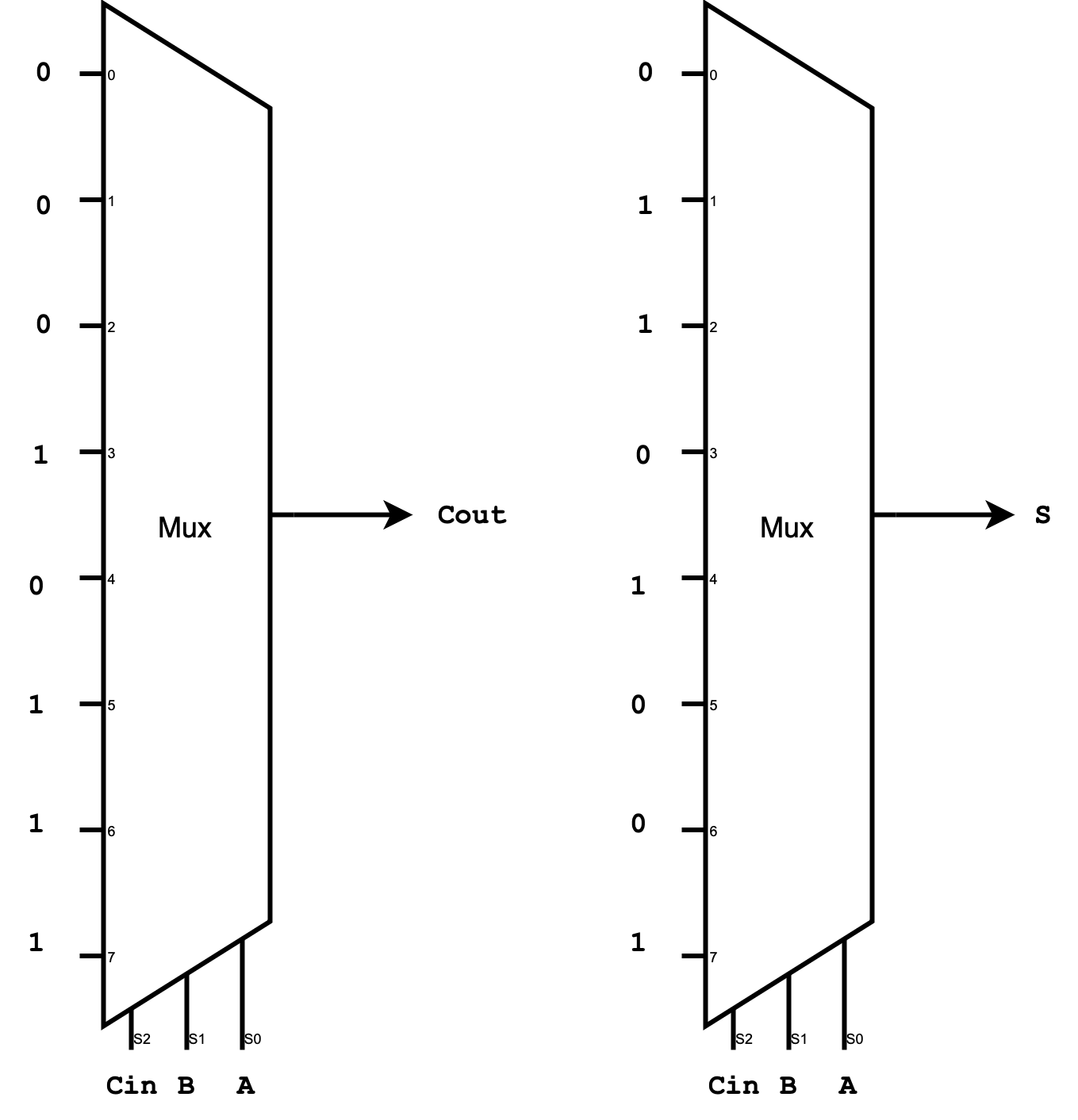
Multiplexer (shorted as “MUX”) is a special combinational logic device that is very commonly used in practice. It is implemented using basic logic gates (INV, AND, and OR, or NANDs). The MUX is expensive to manufacture, but universal, meaning that it can implement any boolean function because essentially it “hardcodes” the truth table.
The symbol for a MUX is as shown in the image below. The truth table is written at the side. A MUX always has three types of terminals:
- \(2^k\) bits data inputs,
kbits selector signal(s) –this is also an input, but we have a special name for them them: selector– , and- 1-bit output.
It’s function components: the inputs, the selector signal(s), and the output. It basically “allows” one of the input signals to pass through when selected to be reflected at OUT.
For example in the case of 2-input MUX below, when S=0, it will reflect whatever value the signal \(A\) carries (1 or 0) as its output:
Take some time to make sense of the truth table. That is if S=0, OUT = A. Else, if S=1, OUT = B. produce the signal \(D_0\) as its output:

You can build a 2-input multiplexer using basic gates:

Some properties about multiplexers:
- Muxes are universal, meaning that it can implement any boolean functions
- A Mux can have \(2^k\) data inputs, and \(k\) bits select inputs, and only can have 1 output terminal.
We can also generalise the multiplexer to take more inputs: 4, or 8, or 16, etc. We can either build a bigger multiplexer from scratch or cascade many 2-input multiplexers. The following figure shows an example of a 4-input multiplexer, implemented as a big MUX (left) or using a series of 2-input MUX (right):

Similarly, you can build a 4-input MUX using basic logic gates:

Using Mux to implement 1 bit FA
Below is an example of how a MUX can be used to implement a more complex combinational device, the full adder that we encounter in the lab. The truth table of a full adder is as shown, it is basically an addition (of three inputs) in base 2:
| A | B | Cin | Cout | S |
|---|---|---|---|---|
| 0 | 0 | 0 | 0 | 0 |
| 0 | 0 | 1 | 0 | 1 |
| 0 | 1 | 0 | 0 | 1 |
| 0 | 1 | 1 | 1 | 0 |
| 1 | 0 | 0 | 0 | 1 |
| 1 | 0 | 1 | 1 | 0 |
| 1 | 1 | 0 | 1 | 0 |
| 1 | 1 | 1 | 1 | 1 |
The multiplexer can simply implement the truth table by mapping each type of output bit \(C_{out}\), and \(S\) in each of the input terminals of the MUX as illustrated below:
While it is convenient to use MUXes to implement any combinational logic device by directly mapping its truth table, this approach is not ideal in practical hardware design.
First, a full adder implemented with logic gates (AND, OR, XOR) is typically more efficient in terms of propagation delay, as a dedicated gate-based circuit can compute outputs in fewer logic levels compared to a MUX implementation that must decode and select values.
Second, a traditional gate-based design is more scalable, as cascading MUX-based full adders can quickly become impractical when implementing larger adders (e.g., ripple-carry or carry-lookahead adders), whereas logic gates naturally extend to these architectures.
Comparison
This section compares the size (and cost) of making 1-bit FA through various methods:
- Straightforward logic synthesis (SOP)
- Logic synthesis after minimisation
- NAND-gates only synthesis
- Using multiplexer
Recall: NAND gates are made up of 4 transistors, and INV is made up of 2 transistors.
Let’s compare the size of the 1-bit Full Adder using each implementation.
Straightforward implementation based on SOP
The SOP of 1-bit FA is:
\[\begin{align} S &= \bar{A}\bar{B}C_{in} + \bar{A}B\bar{C_{in}} + A\bar{B}\bar{C_{in}} + ABC_{in} \\ C_{in} &= \bar{A}BC_{in} + AB\bar{C_{in}} + A\bar{B}C_{in} + ABC_{in} \end{align}\]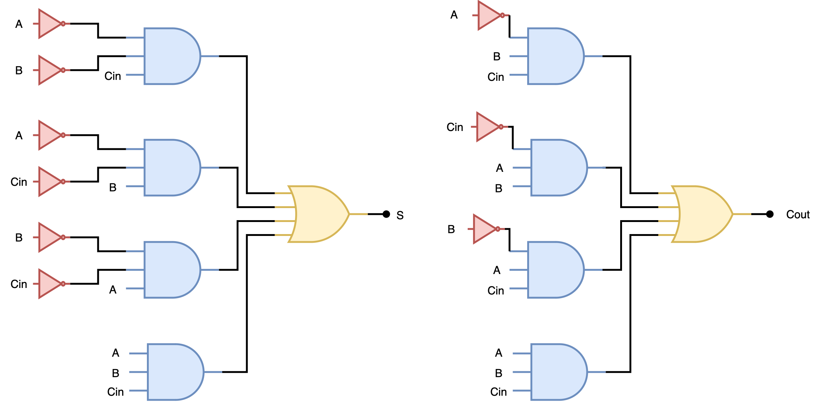
This uses 94 transistors on average.
After minimisation
The Sum bit of an FA can be implemented with XOR gates:
\[\begin{align} S &= \bar{A}\bar{B}C_{in} + \bar{A}B\bar{C_{in}} + A\bar{B}\bar{C_{in}} + ABC \\ &= A \oplus B \oplus C \end{align}\]The Cout bit can be minimised further using a mixture of laws (absorption, distributive, complement, and identity):
\[\begin{align} C &= \bar{A}BC_{in} + A\bar{B}C_{in} + AB\bar{C_{in}} + ABC \\ &= BC_{in}(\bar{A}+A) + A\bar{B}C_{in} + AB\bar{C_{in}} \\ &= BC_{in} + A\bar{B}C_{in} + AB\bar{C_{in}} \\ &= C_{in}(B+A\bar{B}) + AB\bar{C_{in}}\\ &= C_{in}(B+A) + AB\bar{C_{in}} \\ &= C_{in}B + C_{in}A + AB\bar{C_{in}}\\ &= C_{in}B + A(C_{in} + B \bar{C_{in}})\\ &= C_{in}B + A(C_{in}+B) \\ &= C_{in}B + AC_{in} + AB \end{align}\]Full adder implementation using basic logic gates is according to the minimised logic above is:
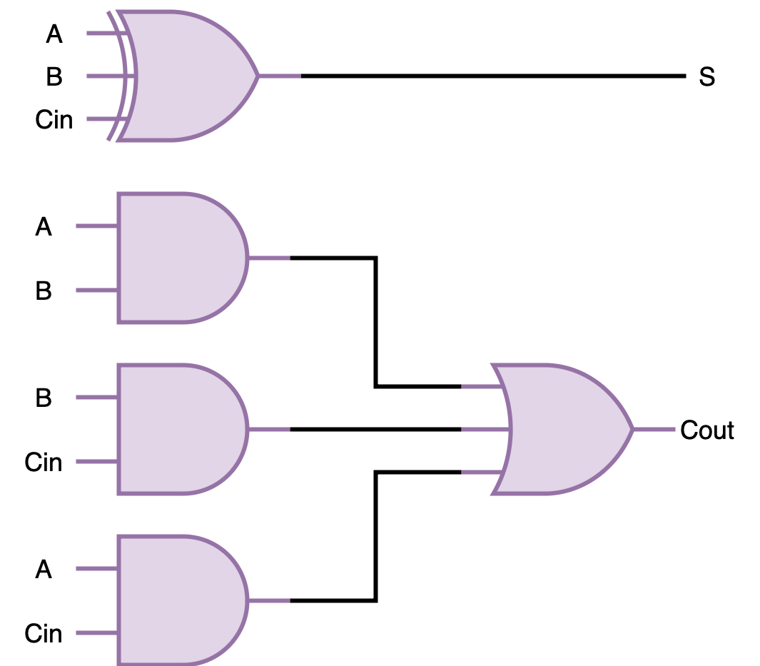
This uses on average 42-48 transistors, depending on how optimised is the 3-input XOR gate:
- 1 3-input XOR gate: 18-24 transistors
- 3 2-input AND gates: 18 transistors
- 1 2-input OR gate: 6 transistors
NAND gates only
It can also be implemented using all NAND gates since NAND gates are universal:
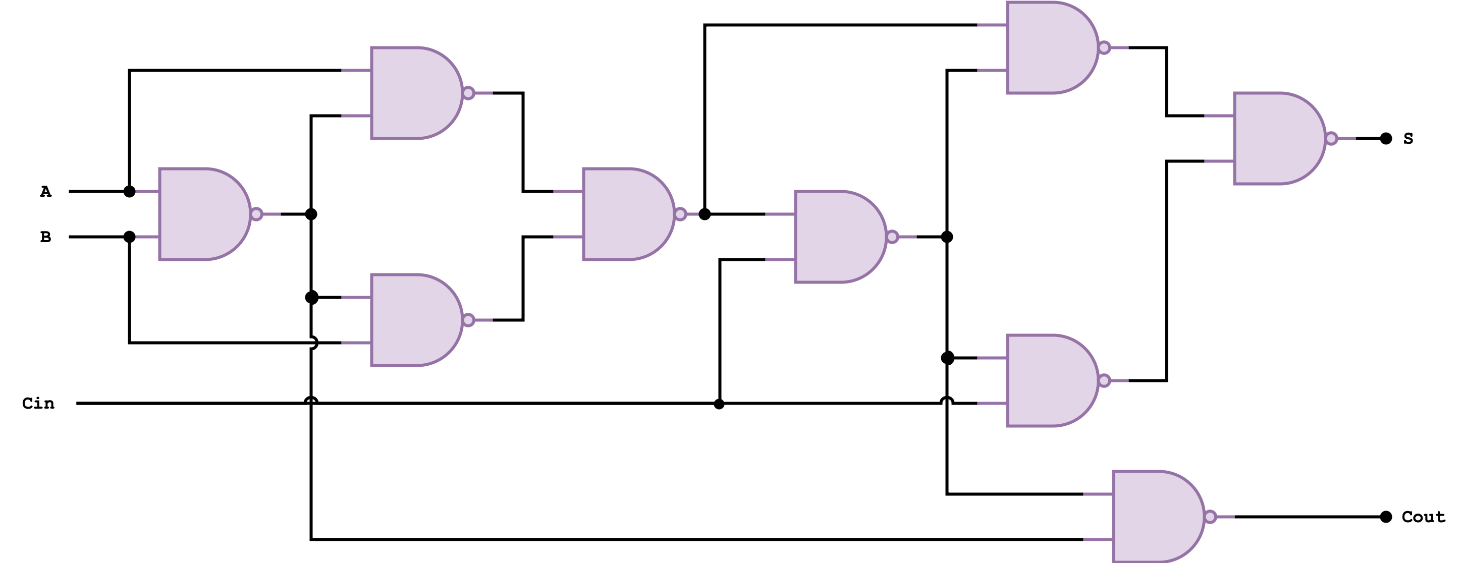
This uses on average 36 transistors on average (9 2-input nand gates). Implementation can be tricky, but there exist clear pattern(s) to follow. It is out of our syllabus.
Using Multiplexers
Finally, the design with two 3-select MUXes (two 8-to-1 MUXes) require 160 transistors on average (approximately 80 transistors to implement each MUX)
From the comparison of different implementations of a 1-bit full adder, we can observe a clear tradeoff between circuit complexity, transistor count, and design approach. Choosing the right logic implementation can significantly impact the power, area, and performance of the circuit
Demultiplexer
A demultiplexer (deMUX) is a combinational routing circuit that takes one input channel (where channel can be more than 1-bit wide) and directs it to exactly one of N output channels, selected by k select lines (typically N = 2^k).
Channel is the key word: the deMUX does not have to route only a single wire. The input can be 1 bit or a w-bit bus.
There are two common formal definitions of a demultiplexer:
- 1-to-N, 1-bit deMUX (common in this course)
- Input:
D - Outputs:
Y0..Y(N-1) Yi = D · decode_i(S)
- Input:
- 1-to-N, w-bit deMUX (less common)
- Input:
D[w-1:0] - Outputs:
Y0[w-1:0] .. Y(N-1)[w-1:0] Yi[b] = D[b] · decode_i(S)for each bitb
- Input:
The gate-level schematic of a 1-select input 1-bit deMUX and its corresponding symbol is:
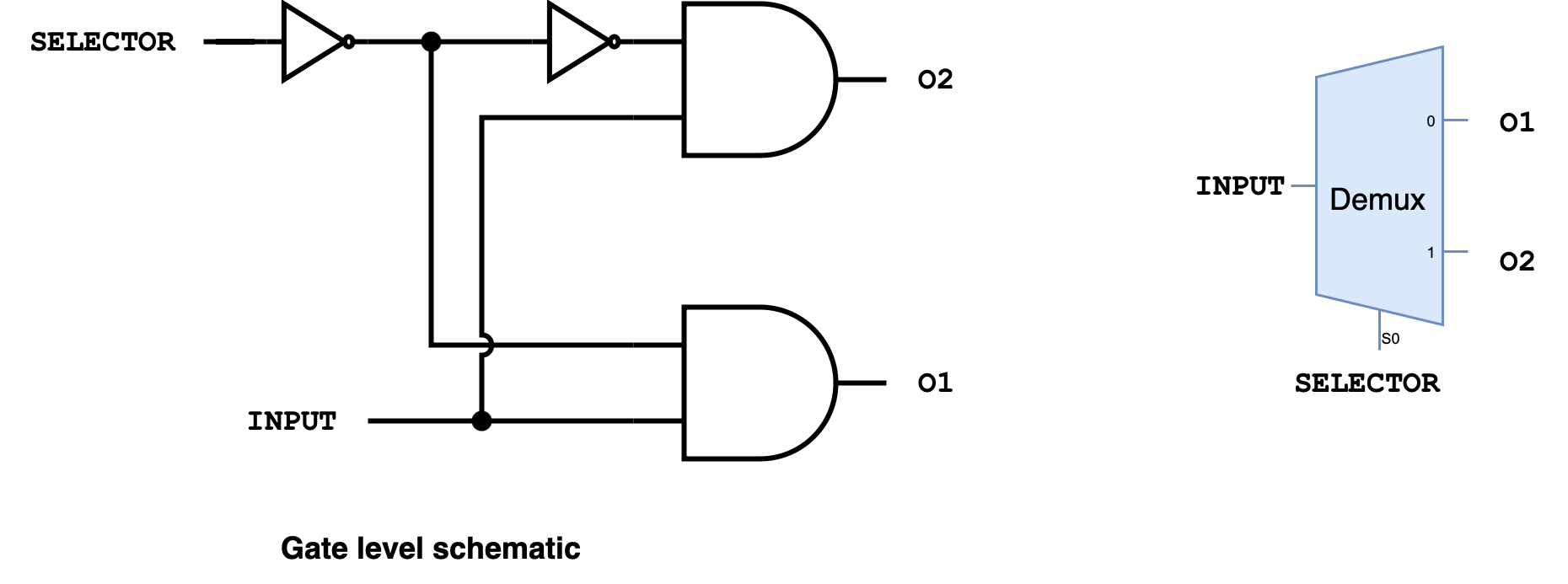
Practice
Draw out the truth table of the demultiplexer above.
Decoder
A common subset of a deMUX is a decoder, as both circuits use select inputs to determine which output is activated. However, while a decoder simply activates one of its outputs based on the input combination, a deMUX not only selects an output but also forwards the input data to the selected output.
The schematic of a 2-select inputs decoder: \(S_0\) and \(S_1\) is:
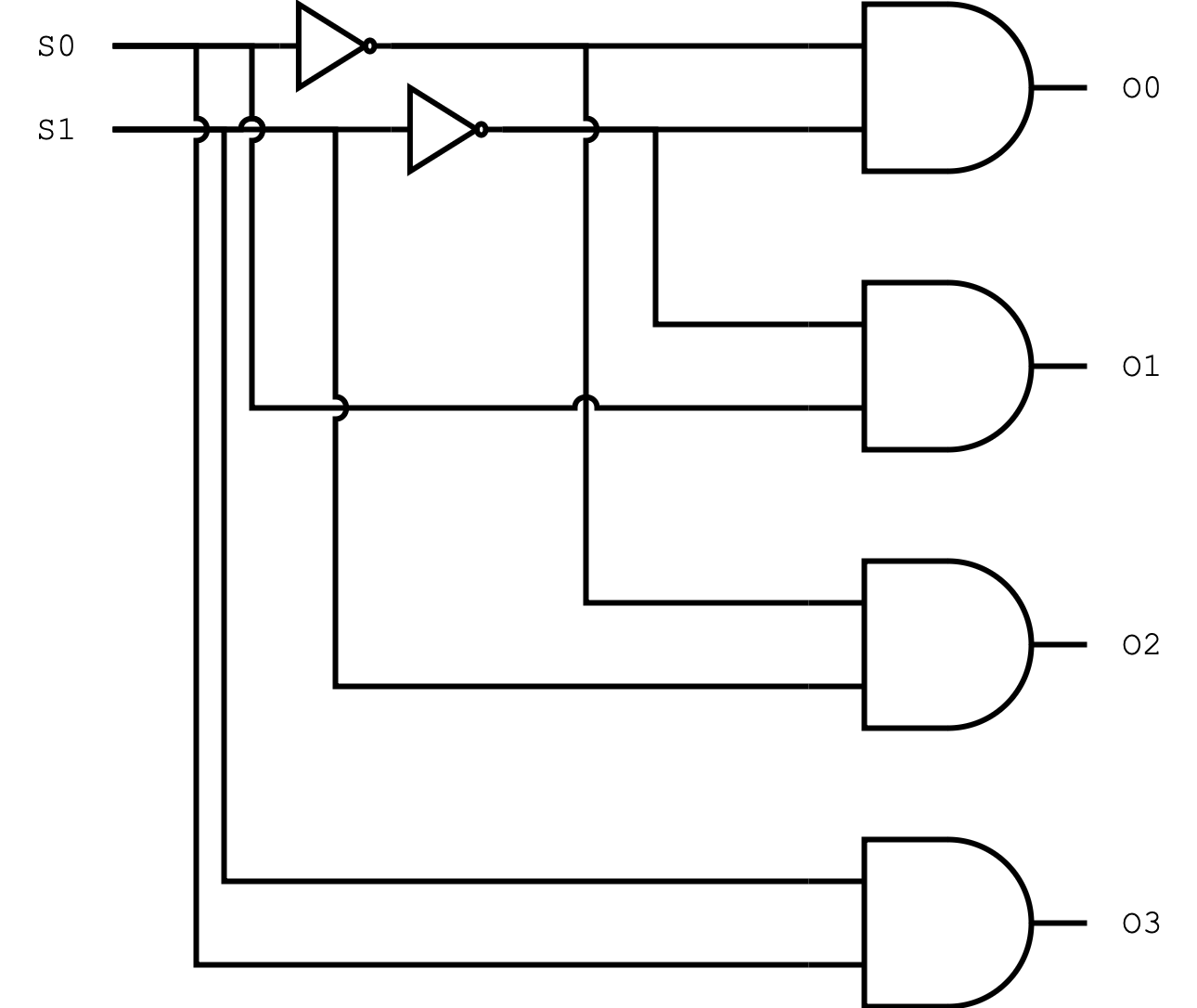
Take some time to trace out the selector values to the output and draw out a truth table for the decoder/deMUX. Do not worry about the logic gate schematics of a decoder. It is only there to show you that a decoder is made up of the normal logic gates like inverters and AND gates.
Properties
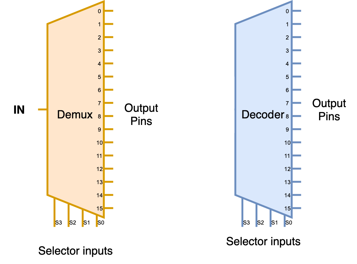
- The symbol of a decoder/deMUX is shown as above
- A deMUX is technically the opposite of a multiplexer. It has \(k\) select inputs, and \(2^k\) possible data outputs, and only 1 bit of input to forward.
- A decoder does not “forward” any input, but instead only activates one of the output lanes.32. At any given time only 1 bit of the \(2^k\) output bits can be
1(high). This is apparent when we try to draw the truth table for a \(k\) input decoder.
For example, the truth table for a 1-selector bit decoder is:
\[\begin{matrix} S & O_1 & O_2\\ \hline 0 & 1 & 0 \\ 1 & 0 & 1\\ \hline \end{matrix}\]The truth table for a 2-selector bits decoder is:
\[\begin{matrix} S_1 & S_0 & O_0 & O_1 & O_2 & O_3\\ \hline 0 & 0 & 1 & 0 & 0 & 0 \\ 0 & 1 & 0 & 1 & 0 & 0 \\ 1 & 0 & 0 & 0 & 1 & 0 \\ 1 & 1 & 0 & 0 & 0 & 1 \\ \hline \end{matrix}\]Only the selected output bit \(i\) is HIGH ( 1), and the rest of the \(2^k-1\) data output is LOW (0).
Read-Only-Memories (ROM)
One of the application of a decoder is to create a read-only-memories (ROM). You can buy them online, like this product.
For example, if we “hardcode” the Full-Adder using a decoder, we end up with the following ROM design:

Explanation of the schematic above:
- At the output of the decoder, we have a pulldown circuit (an NFET connected to ground), which will “drain” a signal into LOW (
0). - Recall that at each combination of select signal \(A, B\), and \(C_i\), only one of the 8 outputs of the decoder will be
1. - The vertical wire with the VDD and the decoder output is not connected (has no relationship) except for those joined by the NFETs.
For example, when \(A=0, B=0, C_{in}=1\), the second output line of the decoder from the top, highlighted in blue in the image below is set to 1:

- Since there exist a pulldown at the S line, it drains the
1and results in0at S line towards the inverter. There’s no pulldown for the \(C_{out}\) line, so the value fed in towards the inverter in the \(C_{out}\) line is1. The inverter invert these values as their final output. - Therefore, when \(A=0, B=0, C_i=1\), \(S\) is
1and \(C_{out}\) is0.
In a ROM (Read-Only Memory) array using NFETs to pull down word lines, the presence of a pulldown (NFET turning ON) is interpreted as a logical ‘0’. However, since ROMs typically output data in an active-high format (1s and 0s directly), we need inverters to flip the signals correctly.
Note the presence of inverters by invention at the end of the two vertical output lines for \(S\) and \(C_{out}\), so the overall output is inverted to be
1for \(S\) and0for \(C_{out}\).NFETs are preferred instead of PFET in a ROM design because they have lower resistance when ON, enabling faster and more power-efficient pull-down operation.
The location of the “pulldown” circuits correspond to a 1 in the truth table for that particular output (\(S\) or \(C_{out}\)). For \(K\) inputs, decoder produces \(2^K\) signals, only 1 which is asserted (valid “High”, or simply “selected”) at a time. The properties of ROM are as follows:
- ROMs ignore the structure of combinational functions (our truth table is “hardcoded”)
- The selectors are the address of an entry.
- For an \(N\)-input boolean function, the size of ROM is roughly \(2^N \times \text{#outputs}\).
For example, the Full Adder has 3 inputs (A, B, \(C_{in}\)), and 2 outputs (\(S\) and \(C_{out}\)). Hence the size of the ROM is \(2^3 * 2 = 16\).
ROM is a also universal tool for implementing combinational logic functions but may not always be practical for functions with a large number of inputs due to memory size constraints.
Summary
You may want to watch the post lecture videos here.
Here are the key points from this notes:
- Multi-input logic gates: There are 16 2-input logic gates (AND, XOR, XNOR, etc), and there are $2^{2^x}$ possible $x$ input gates.
- Synthesize logic: Given a truth table, perform straightforward logic synthesis using sum-of-products.
- Boolean Algebra Minimisation: Minimise boolean functions (e.g: basic sum-of-products) using DeMorgan’s theorem, reduction rule, absorption rule, etc or Karnaugh Map to make the boolean equation more compact. This results in simplified hardware (cheaper, smaller) while retaining functionality.
- Universal Gates: NAND and NOR gates are universal. We can construct any combinational logic device by just using NAND gates or NOR gates alone.
- Complex Combinational Logic Device: Special devices like deMUX, decoder, multiplexer, and ROM are essential components. Multiplexers are used to implement conditional logic (if-else), decoders are used to perform address decoding among many others. Decoders can be used to implement a ROM. It maps the input address lines to specific memory locations within the ROM.
- Universal Logic Synthesizer: Both ROMs and Muxes are universal logic synthesizer and can be used to implement any logic. ROM essentially acts as a look-up table (LUT) where each input combination maps directly to a pre-defined output value. However, this results in size explosion. For $n$ inputs, the ROM requires $2^n$ rows, leading to rapid growth in memory size for large input sizes. Mux-based designs do not suffer from exponential size explosion in the same way. A MUX scales hierarchically, where smaller MUXes can be used to build bigger MUXes in a structured way rather than requiring an exponentially growing number of components like ROMs do.
Design tradeoff summary for logic synthesis:
- ROM-based designs (easiest, simply store the truth table as-is) are useful when precomputed logic storage is acceptable and logic complexity is high.
- Mux-based designs are more efficient for small, optimized logic designs due to their faster and smaller implementation.
- SOP design is useful when a direct and systematic Boolean implementation is needed, making it ideal for medium-complexity logic functions.
- NAND-gate-based design is useful when minimizing component types is important, as NAND is a universal gate that can implement any logic efficiently.
- Finally, highly optimized gate-level design (most difficult) is useful when minimizing transistor count, power consumption, and delay is critical for high-performance applications.
Designing and implementing the logic directly using gates like AND, OR, NOT, NAND, NOR, etc., rather than relying on a ROM to store the outputs leads to a more efficient design (smaller unit, cheaper unit, less power drawn), but it is challenging to do so and to test because it is prone to errors.
Studying boolean algebra and minimization is essential for optimizing SOP-based and gate-level designs, reducing the number of gates, transistors, power consumption, and delay for more efficient implementations.
You won’t be required to design or draw circuits from scratch in this course. Instead, you’ll be given pre-designed circuits, and your task will be to analyze and trace their behavior.
Appendix
Logic Synthesization with CMOS
We can create a combinational logic device easily given the minimized boolean expression, using any of the universal gates:
- NANDs only
- NORs only
- AND, INV, and OR
Each gate can be created using transistors: PFETs and NFETs arranged in a complementary way. The schematic of each is as follows:

The OR and AND gates are simply the NOR and NAND gates with inverter at the output.
We can also create the device straight using CMOS recipe given the minimised boolean expression (instead of using the universal gates). For example, given this minimised equation that we did earlier: \(Y= \overline{C} A + CB\)
It can be made this way with a combination of universal gates:
Recall that the AND is actually NAND + INV, and the OR is NOR + INV.

This requires 20 MOSFETs to build.
The freestyle way
You may design CMOS circuitry without any rules. It’s a little like an artwork and theres more than one way to construct the circuit that produces the same logic. You can choose to construct the pull-down first or the pull-up first. You can also choose to construct the negation of the circuit and invert the overall output. Please do not memorise this blindly. At the end of the day, whichever method you choose, it is fine as long as the CMOS circuit produces the correct logic. If you want to minimise them though them some careful design is required. It is an art to design a CMOS circuit and it is beyond the scope of this course.
- Step 1: Construct a pull-down circuitry:
- for each ‘+’ (OR) we build a parallel NFET circuit
- for each \(\cdot\) (AND) we build a series NFET circuit
Therefore we have two sets of two NFETs in series:

- Step 2: Add inverter at the output.
- In Step 1 we created a pull-down circuitry that is activated when each of the terms in the boolean expression produces an overall
1. - E.g: when \(B, C\) are both 1, the pull-down is activated as current can flow from \(Y\) to the GND. The effective output at \(Y\) will be then
0when \(B,C\) are both1. - Since what we want is the opposite, we need to put an inverter at the output, that is \(Y=1\) when \(B,C\) are both 1, we need to put an inverter at the output, as shown:

If what you want is for \(Y\) to be
0when \(B,C\) are both1then there’s no need to put an inverter in the end. Just draw the complementary pullup and call it a day - In Step 1 we created a pull-down circuitry that is activated when each of the terms in the boolean expression produces an overall
- Step 3: Construct the complementary pull-up circuitry and assemble. Refer to the CMOS recipe in the previous chapter.

This requires 14 MOSFETs to build, less than the previous design. It is definitely easier (for us) to create a combinational logic device using a bunch of universal gates, but it comes at the cost of money and size.
Note that the CMOS recipes that we learn in this course also does not guarantee that you can build a device with minimised number of transistors, given its functional specification. It is an art to create the most efficient circuit in terms of money, size, and usage.