 50.002 CS
- Combinational Logic Timing (Basic)
- Tracing CMOS Circuit (Basic)
- Universal Gates (Basic)
- Full Adder Timing Analysis (Intermediate)
- Combinational Construction Rules (Intermediate)
50.002 Computation Structures
Information Systems Technology and Design
Singapore University of Technology and Design
CMOS Technology
Each topic’s questions are grouped into three categories: basic, intermediate, and challenging. You are recommended to do all basic problem set before advancing further.
Combinational Logic Timing (Basic)
Consider the following combinational logic device.
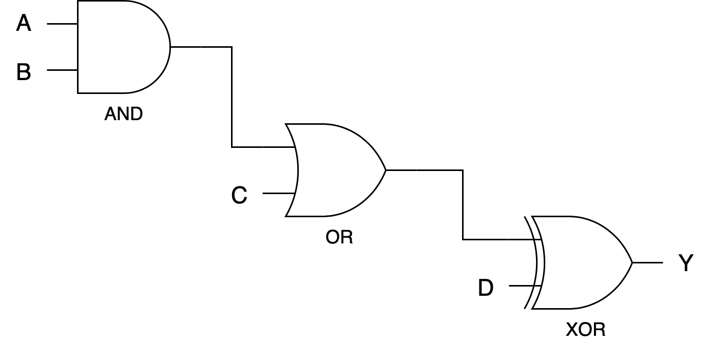
Each logic gate has the same:
- Propagation delay, tpd= 2ns,
- Contamination delay, tcd=1ns
Compute the overall propagation delay and contamination delay for the circuit.
Overall **tpd** = 6ns (counting paths from the AND gate, OR gate, and XOR gate).
Overall **tcd** = 1ns (counting the shortest path from XOR gate).
Tracing CMOS Circuit (Basic)
Draw the truth table for the following CMOS circuitry:
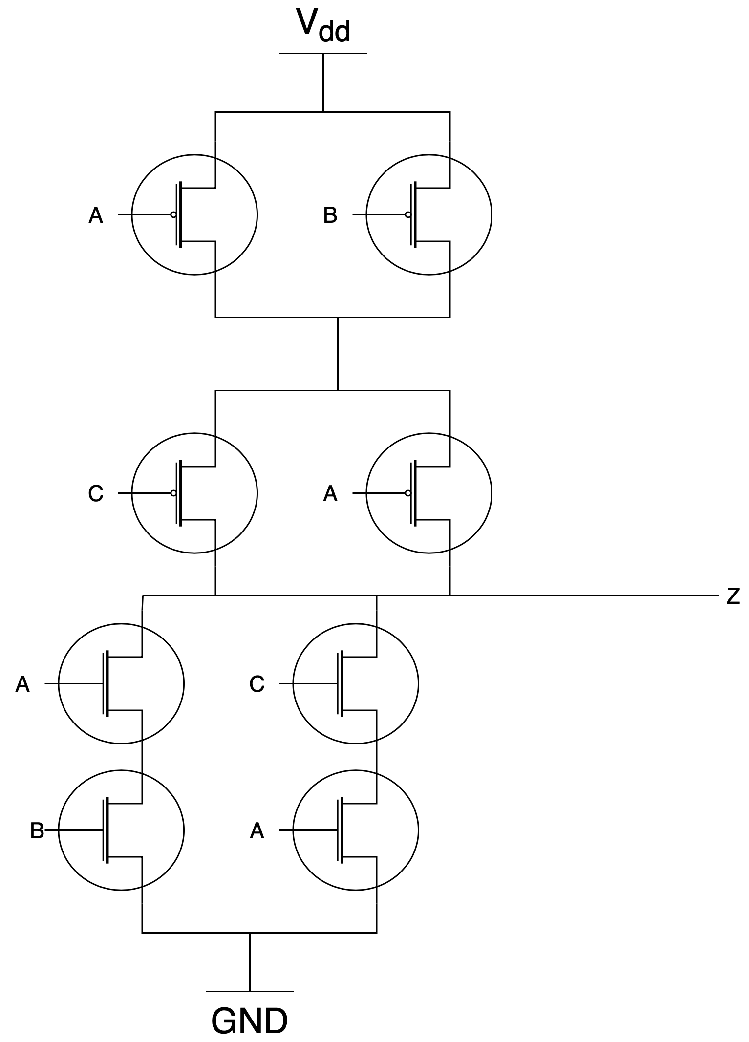
$$ \begin{matrix} A & B & C & OUT \\ \hline 0 & 0 & 0 & 1 \\ 0 & 0 & 1 & 1 \\ 0 & 1 & 0 & 1 \\ 0 & 1 & 1 & 1 \\ 1 & 0 & 0 & 1 \\ 1 & 0 & 1 & 0 \\ 1 & 1 & 0 & 0 \\ 1 & 1 & 1 & 0 \\ \hline \end{matrix} $$
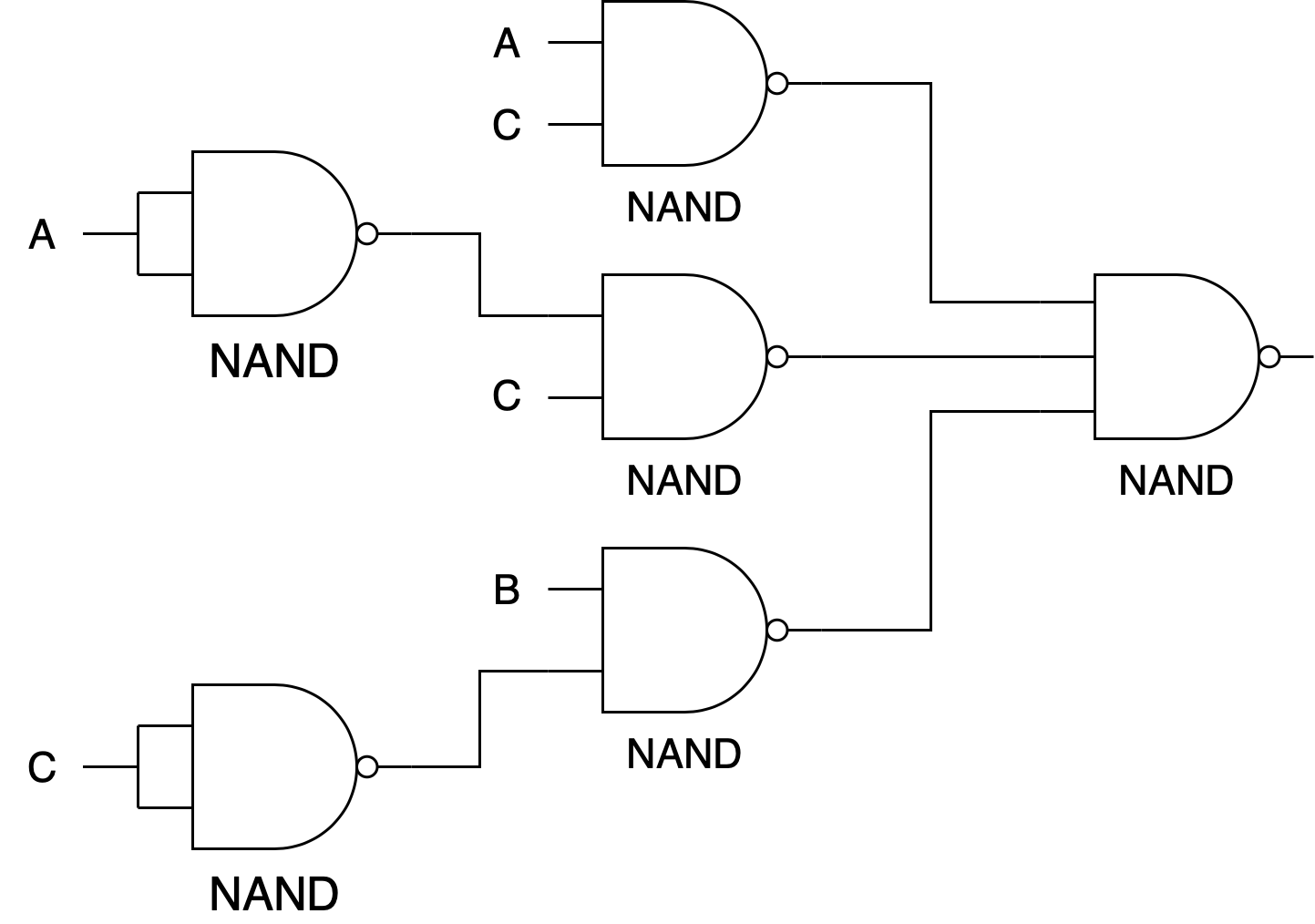
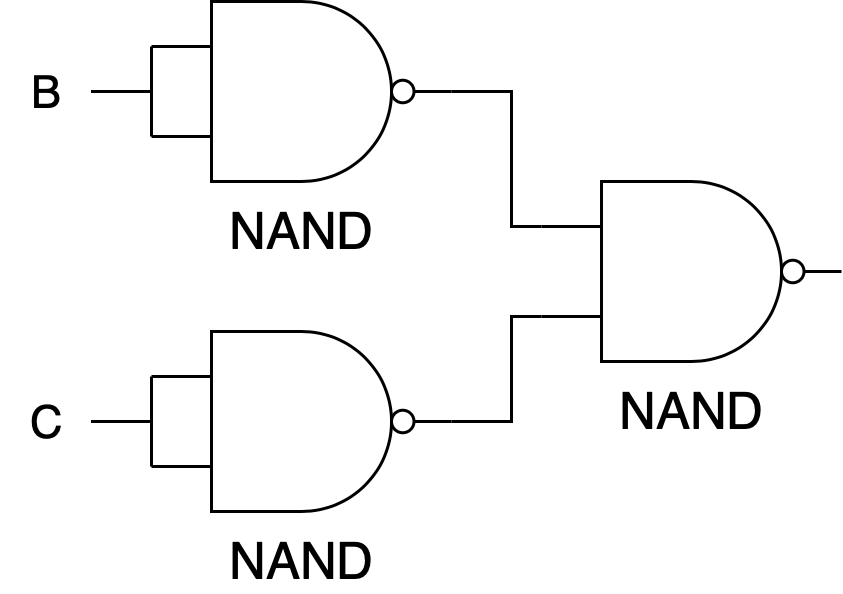
Universal Gates (Basic)
Use only NAND gates to redraw the circuit below. Use as few NAND gates as possible.
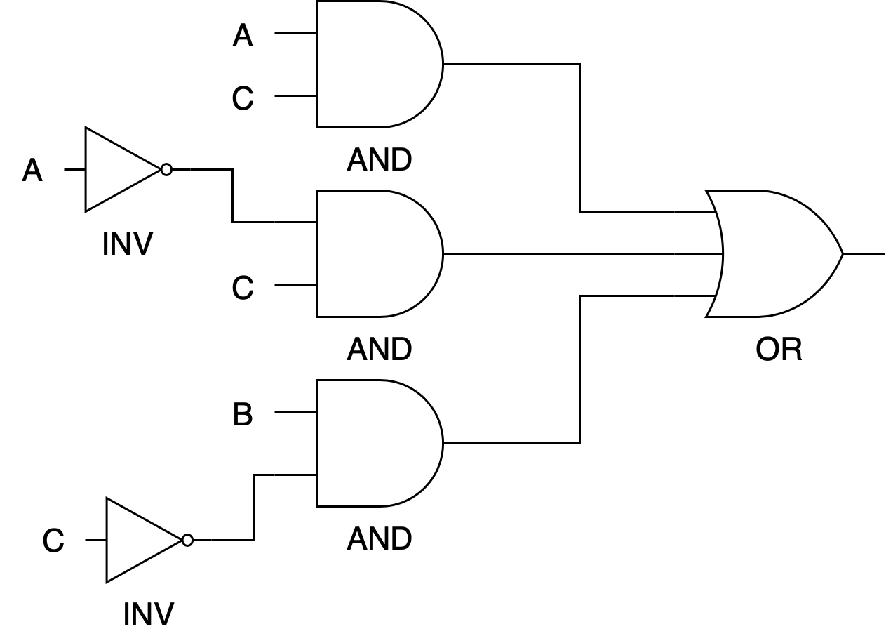
Think!
How many MOSFETs do we save by minimising the boolean expression first before realising it into hardware?
If you directly convert with just NAND gates then you'll get:
You can minimise them first by minimising the boolean expression: $$AC + \bar{A}C + B\bar{C} = C+B\bar{C} = C + B = \overline{\bar{C}\bar{B}}$$
Then we can easily draw the circuitry for the minimised expression:
Full Adder Timing Analysis (Intermediate)
Refer to the FA circuitry below:
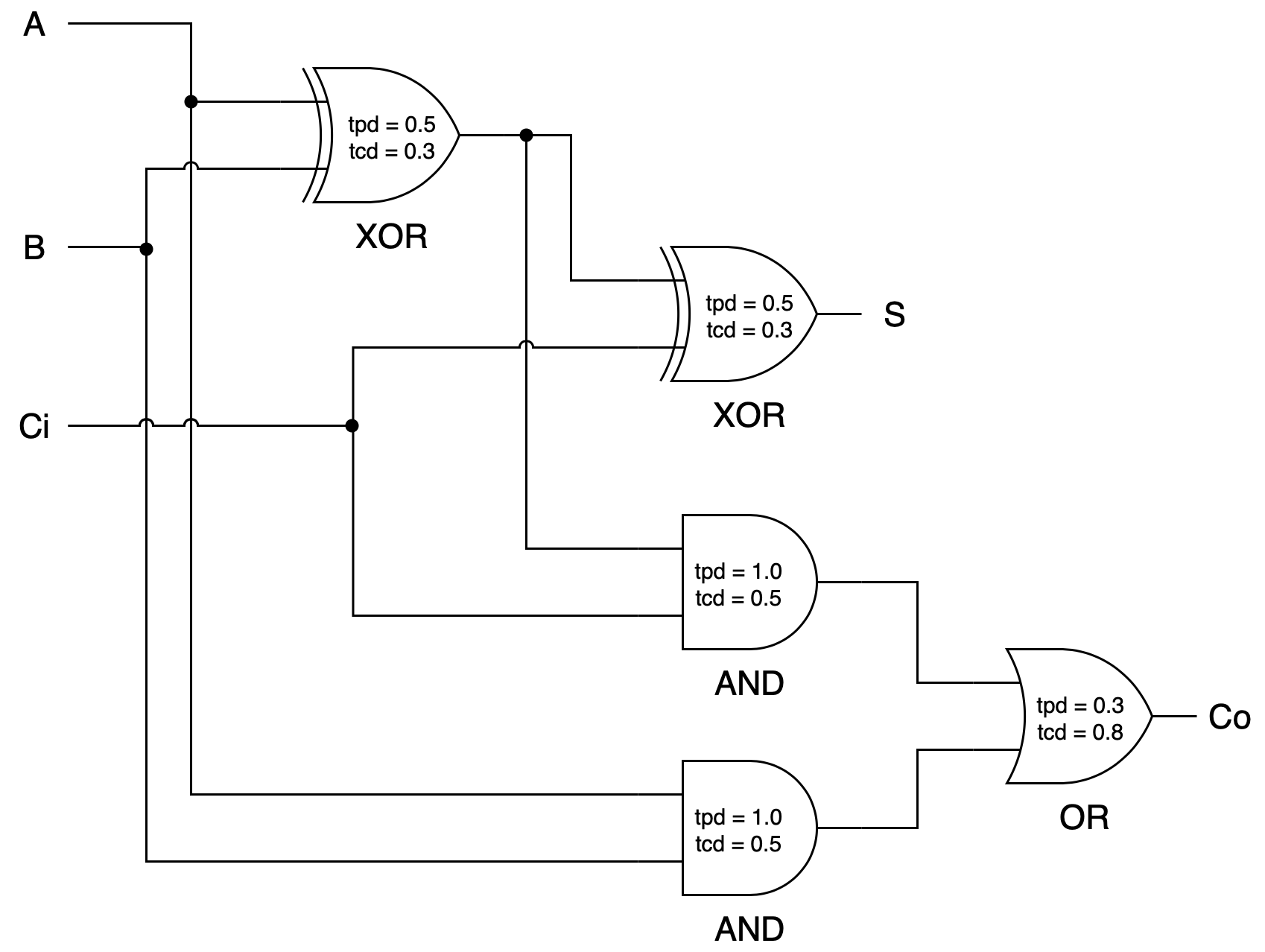
Answer the following questions:
- Compute the tpd and tcd of the full adder above.
-
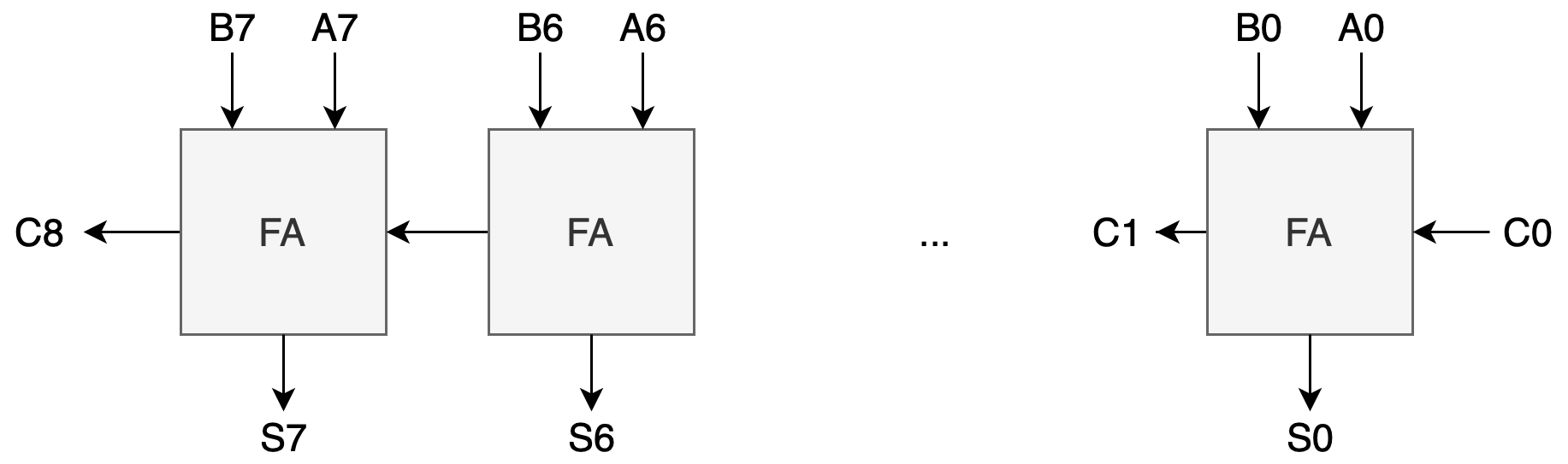
If we were to put several of these FAs to form an 8-bit ripple-carry adder as shown, compute the tpd and tcd of an 8-bit ripple-carry adder made of 8 of these FA circuits.
- The **tpd** is 1.8 and the **tcd** is 0.3 for a single FA.
- For the 8-bit ripple-carry adder, one might think at first that its **tpd** is simply 8 times bigger than a single FA, that is 14.4. However, note that inputs **Ai**, **Bi** are given as a valid signal at the **same time** for all adder units: $$i=0,1,...7$$ That means **Ai** XOR **Bi** computation for all units happen *in parallel* during the first 0.5ns only. Hence, the **tpd** of the 8-bit RCA is: $$1.8+7\times1.3=10.9$$ The contamination delay of the 8-bit RCA remains at 0.3ns.
Combinational Construction Rules (Intermediate)
During lecture, we learned a first set of principles that define a combinational device. A combinational device is a circuit element that has:
- One or more digital inputs.
- One or more digital outputs.
- A functional specification that details the value of each output for every possible combination of valid input values.
- A timing specification consisting (at minimum) of an upper bound tpd on the required time for the device to compute the specified output values from an arbitrary set of stable, valid input values.
We also learned a second set of rules, that a set of interconnected elements is a combinational device if:
- Each circuit element is combinational.
- Every input is connected to exactly one output or to some vast supply of 0’s and 1’s.
- The circuit contains no directed cycles.
Read point (2) carefully. This does NOT mean that a combinational device must just have one output and one input. This means that for each input of a combinational device, it is connected to exactly ONE output of the “previous” device.
In this problem, we ask you to think carefully about why these rules work - in particular, why an acyclic circuit of combinational devices, constructed according to the second principle, is itself a combinational device as defined by the first.
Consider the following 2-input acyclic circuit whose two components, A and B, are each combinational devices.
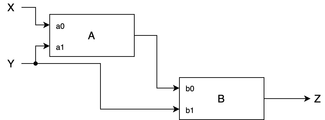
The propagation delay for each device is specified in nanoseconds:
- Device A tpd: 3ns
- Device B tpd: 2ns
The functional specifications for each component are given as truth tables detailing output values for each combination of inputs, where \(A _{a_0, a_1}\) denotes the output from device A, and \(B _{b_0, b_1}\) denotes the output from device B:
\[\begin{matrix} a_0 & a_1 & A _{a_0, a_1} & b_0 & b_1 & B_{b_0, b_1}\\ \hline \\ 0 & 0 & 1 & 0 & 0 & 0\\ 0 & 1 & 0 & 0 & 1 & 0\\ 1 & 0 & 0 & 1 & 0 & 0\\ 1 & 1 & 1 & 1 & 1 & 1\\ \hline \end{matrix}\]Answer the following questions:
- Give a truth table for the overall acyclic circuit, i.e. a table that specifies the value of z for each of the possible combinations of input values on x and y.
- Describe a general procedure by which a truth table can be computed for each output of an arbitrary acyclic circuit containing only combinational components. Hint : construct a functional specification to each circuit node.
- Specify a propagation delay (the upper bound required for each combinational device) for the circuit.
- Describe a general procedure by which a propagation delay can be computed for an arbitrary acyclic circuit containing only combinational components. Hint: add a timing specification to each circuit node.
- Do your general procedures for computing functional specifications and propagation delays work if the restriction to acyclic circuits is relaxed (lifted)? Explain.
- The truth table is as follows: $$\begin{matrix} X & Y & Z \\ \hline 0 & 0 & 0 \\ 0 & 1 & 0 \\ 1 & 0 & 0 \\ 1 & 1 & 1 \\ \hline \end{matrix}$$
- We can construct the truth table from left to right, i.e: solve the truth table for each component from the leftmost (inputs) all the way to the rightmost (outputs), one by one.
- The total propagation delay is the sum of each device's (A and B) propagation delay. This amounts to: $$3 + 2 = 5ns$$
- We have to find the longest path from (any) input to (any) output to find the total propagation delay of the combinational circuit.
- No, the signal can propagate back into the circuit's input so using the longest path to calculate **tpd** is not applicable anymore.