 50.002 CS
- Overview
- The MOSFET Overview
- Types of MOSFETs
- Switching NFETs and PFETs ON/OFF
- Complementary MOS circuitry
- The CMOS Complementary Recipe
- Logic Gates
- Timing Specifications of Combinational Logic Devices
- Exercise
- Summary
- Appendix
50.002 Computation Structures
Information Systems Technology and Design
Singapore University of Technology and Design
The CMOS Technology
You can find the lecture video here. You can also click on each header to bring you to the section of the video covering the subtopic.
Detailed Learning Objectives
- Explain the Basics of MOSFETs:
- Identify the structure and operation of Metal-Oxide Semiconductor Field-Effect Transistors (MOSFETs).
- Identify the roles of the gate, drain, source, and body in MOSFET operation.
- Differentiate Between NFET and PFET:
- Compare the characteristics and functions of N-type and P-type FETs.
- Learn how NFETs and PFETs are used to implement different logic functions based on their configuration and voltage levels.
- Design Logic Devices using CMOS Technology:
- Explain how Complementary MOS (CMOS) technology utilizes both NFETs and PFETs to create efficient logic circuits.
- Explain the concept of pull-up and pull-down networks within CMOS circuits.
- Analyze the CMOS Complementary Recipe:
- Justify the complementary nature of pull-up and pull-down circuits in CMOS technology to prevent short circuits and ensure stable logic states.
- Apply the complementary MOS circuitry to understand basic logic gates like NAND and NOR.
- Explain Logic Gate Fundamentals:
- Identify different types of basic logic gates and their operations.
- Outline how each logic gate is implemented using CMOS technology to fulfill specific logic functions.
- Analyze Timing Specifications in Combinational Logic Devices:
- Evaluate propagation delay and contamination delay as critical timing specifications in digital circuits.
- Evaluate how these delays impact the performance and reliability of logic circuits.
These objectives aim to provide us with a comprehensive understanding of the basic building blocks of digital electronics, focusing on MOSFETs and their application in combinational logic devices through CMOS technology.
Overview
In this chapter, we are learning a particular component called the MOSFET that can be used as a building block to make combinational logic devices (logic gates and more complex digital systems). CMOS is ideal for combinational devices (that need to obey static discipline) because it provides output voltages that fully span from the supply voltage (Vdd) to ground (Vss), ensuring clear and reliable logic levels.

Image obtained from Lesics
Why MOSFET?
If we connect MOSFETs in a specific way, we can create a combinational logic device that represents our desired truth table or functional logic specification. MOSFETs are used because they can produce reliable logic levels with low power consumption, are cost-effective, and generate minimal heat.
Further supporting characteristics of MOSFET:
- High Noise Margins: Ensures clear distinction between logical 0 and 1, reducing errors.
- Low Static Power Consumption: Prevents excessive heating and power waste in stable states.
- Strong Drive Capability: Can reliably drive subsequent stages without signal degradation.
RECALL: before we continue
The ideal behaviours and characteristics of a combinational logic device are:
- The device should be able to tolerate some amount of errors due to its Noise Margins. The Noise Margin exists if its VTC gain \(>1\).
- If we have high gain, that means we can have more noise margin. Take some time to convince yourself that this is true.
- The device should be cheap, and small sized. We do not want to have bulky devices, do we?
- The device should have zero power dissipation when input voltages aren’t changing. That’s why the device must have a nonlinear gain.
- Otherwise when voltage is changing from,
0to1or1to0, then power within the device has to dissipate easily, meaning that the change is swift, reliable, and quick. We always want our computers to be fast, don’t we?- The device has to be functional, meaning that it conforms to the assigned truth table (logic) at all times. We do not want unpredictable “buggy” behaviour with our devices.
The MOSFET Overview
Metal-oxide semiconductor field effect transistors (MOSFET, or shortened as FETs) is the main material that is used to make our combinational device. The basic schematic of a transistor is shown in the figure below.
MOSFETS are four terminal voltage-controlled switches. You can buy them at a relatively cheap price online for DIY projects. However in computer parts, they are the same components miniaturized to the nanometer scale for high-density integration.

Notable parts of MOSFET and its function:
- MOSFETs are electronic components that control whether a circuit outputs a high (1) or low (0) voltage, forming the basic building blocks of digital devices.
- It has 4 terminals: drain, gate, source, and bulk. Input voltage is supplied at the gate, and output voltage is obtained at the drain.
- Current flow between source and drain \(I_{DS}\) is proportional to \(\frac{W}{L}\) (the width and the length) of the MOSFET.
- Source and drain is physically symmetrical, we name them depending on the type of the MOSFET and the direction of current flow.
- Depending on the input voltage supplied at the gate, a MOSFET can be either ON, allowing current to flow from source to drain, or OFF, leaving the drain with a floating or undefined value.
Remember from your Physics classes:
- Current flows from higher potential (+) to lower potential (-)
- Electron flows from lower potential (-) to higher potential (+)
Current flows between the diffusion terminals (source and drain) if the voltage on the gate terminal is large enough to create a conducting channel (in pink) and the mosfet is on. Otherwise, the conducting channel does not form and the mosfet is off: the diffusion terminals are not connected.
- A MOSFET is said to function as a switch by using the gate voltage to control the formation of a conducting channel between the source and drain.
- Simplified idea: You can connect load (e.g: LED) + power source at the source, and ground at the drain
- Then supply input at the gate to “connect” the source and the drain terminal to turn on the LED
- When the channel forms, current flows (ON state); otherwise, the source and drain are disconnected (OFF state).
MOSFETs are arranged in complementary pairs (PFET and NFET) to form logic gates, where their ON/OFF states control the output voltage. For example, in an AND gate, the transistors are configured so the output is high only when all inputs are high, while in an OR gate, the output is high if any input is high.
Before we learn more about the complementary arrangement of PFETs and NFETs for logic gates, it’s essential to first understand how each type operates individually.
Types of MOSFETs

There are two types of FETs: NFET and PFET as shown above.
- NFET : the majority of the charge carrier for the bulk are holes (p-type semiconductor). The majority of the charge carrier for the source and drain are electrons (n-type semiconductor). Typically, the bulk is connected to GND to keep the PN junction reverse biased.
- PFET : the majority of the charge carrier for the bulk are electrons (n-type semiconductor). The majority of the charge carrier for the source and drain are holes (p-type semiconductor). Typically, the bulk is connected to
VDDto keep the PN junction reverse biased
The circuit symbol for NFET and PFET are shown as above. Note that the bulk of NFET is connected to GND, and the bulk of PFET is connected to VDD, and it is often implied and omitted in circuit diagrams.
Please watch the supplementary video or refer to the later section if you are unclear about what is a PN junction, p-type, or n-type semiconductors.
Some important terms we need to know:
VDD: voltage source- \(V_{TH}\): threshold voltage.
GND: ground- Reverse-biased: a state whereby D is insulated from S, where current cannot flow from D to S in the presence of applied voltage.
- A FET that is “ON” refers to a state whereby there exists a connection between D and S, so that current can flow through them.
- A FET that is “OFF” refers to a state whereby there is no connection between D and S. Current cannot flow through them.
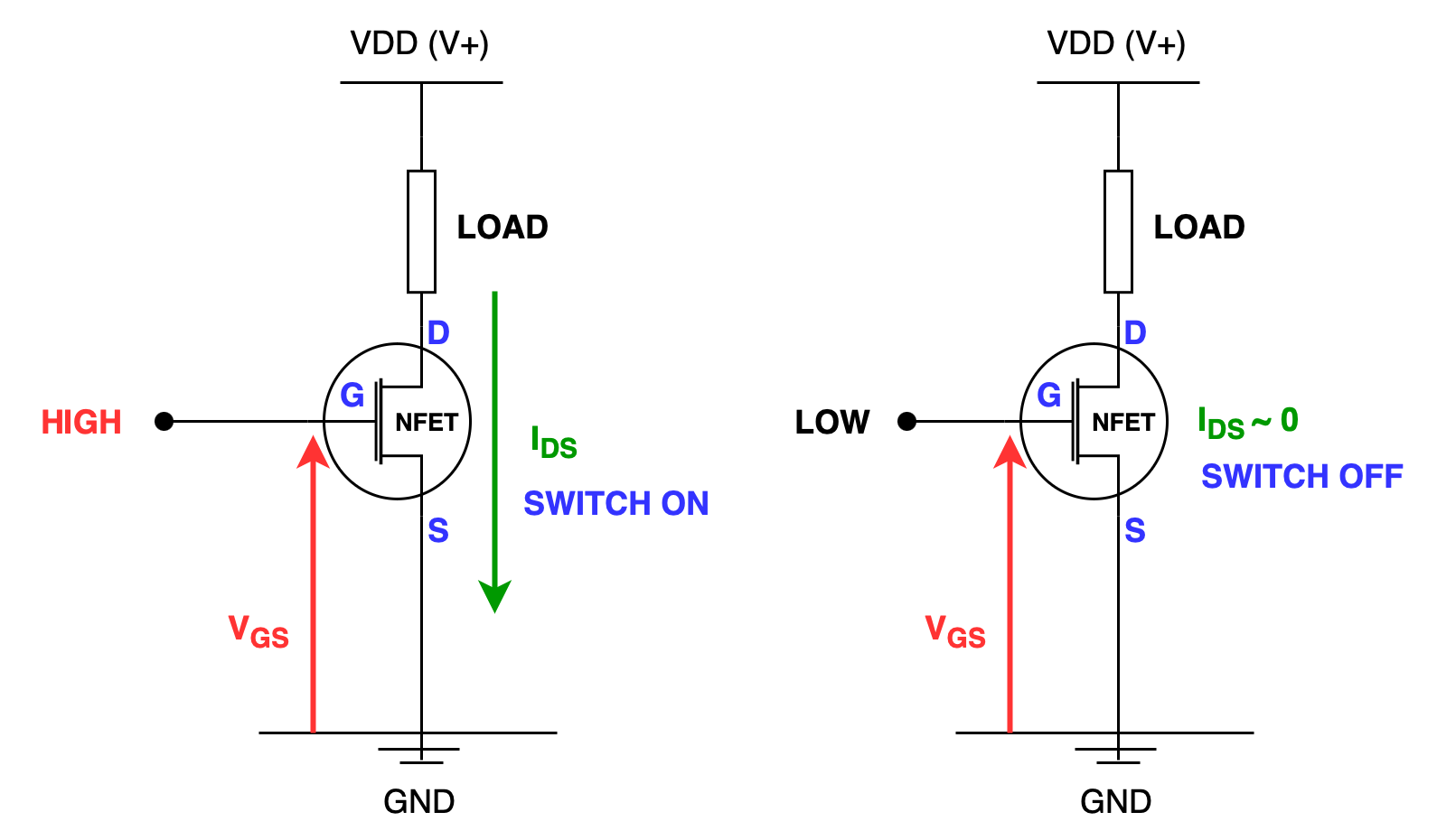
Switching NFETs and PFETs ON/OFF
See the figure below and its corresponding explanation to understand better how NFET and PFET operates. The two drawings on top are PFETS (left: OFF and right: ON). The two drawings below are NFETS (left: OFF and right: ON). You might want to refer to this Figure as well when reading the appendix below.

How NFET operates

- Connections:
- Bulk is connected to
GNDto keep the PN junction reverse biased, meaning that no current should flow or leak between source and bulk and between drain and bulk. - S (and also bulk) is connected to
GNDfor NFET. Current from D is therefore drained toGNDconnected to S.
- Bulk is connected to
- It is “ON” when \(V_{GS} = V_G - V_S\) is high enough. Since source terminal is connected to the
GNDfor NFET,- \(V_{GS} = V_G - 0 = V_G\),
- the NFET is "ON" whenever \(V_G\) is high enough, i.e: \(> V_{TH}\).
- When \(V_G > V_{TH}\), it draws the electrons towards the gate. An n-channel (made of electrons) will be formed between source and drain.
- Note that \(V_{TH}\) for NFET is positive.
- When it is "ON", current can pass from D to S.
- Electron, its majority charge carrier flows from S to D
We can say that its majority charge carrier is drained at D
- The output of an NFET is at the D terminal.
- Hence, the output of an "ON" N-type is
0
- Electron, its majority charge carrier flows from S to D
- It is "OFF" when \(V_{GS}\) is low, as it encourages depletion region to form further.
The figure below summarizes how NFET works as a “switch” that connects the load with the power source and ground:
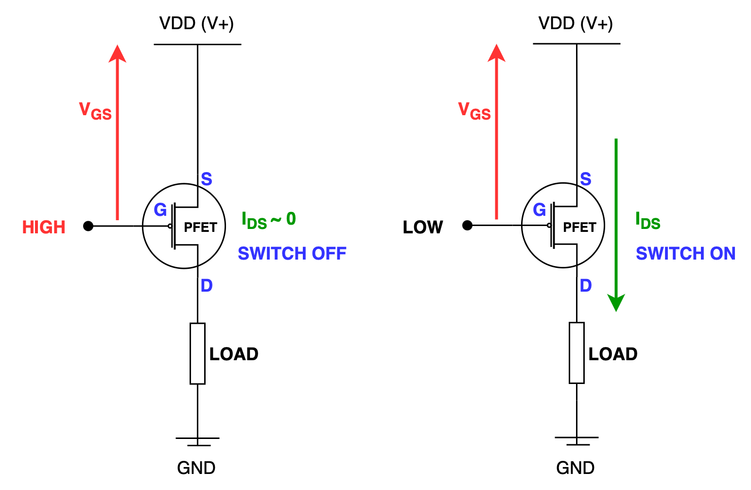
How PFET operates

- The PFET symbol is similar to NFET except that it has the by the bubble \(\circ\). Conversely for its connections:
- Bulk is connected to
VDDto keep the PN junction reverse biased, meaning that no current should flow or leak between source and bulk and between drain and bulk. - S (and also bulk) is connected to
VDDfor PFET. Current can flow from S to D.
- Bulk is connected to
- It is “ON” when \(V_{GS}\) is low enough. Since source terminal is connected to
VDDfor PFET,- \(V_{GS} = V_G - VDD\),
- Hence effectively PFET is "ON" whenever \(V_G - VDD\) is low enough, i.e: \(< V_{TH}\).
- When \(V_G < `VDD` + V_{TH}\) (or equivalently, \(V_{GS} < V_{TH}\)), it draws the holes towards the gate. A p-channel (made of holes) will be formed between source and drain.
- Note that \(V_{TH}\) for PFET is negative.
- When it is "ON", current can pass from S to D.
- Hole, its majority charge carrier flows from S to D.
We can say that its majority charge carrier is drained at D (same as NFET)
- The output of an PFET is also at the D terminal.
- Hence, the output of an "ON" p-type is
1
- Hole, its majority charge carrier flows from S to D.
- It is “OFF” when \(V_{GS}\) is high, as it encourages depletion region to form further.
The figure below summarizes how PFET works as a “switch” that connects the load with the power source and ground:
Summary
MOSFETs operates using voltages. No current flows from the gate towards source/drain since the gate is insulated from source and drain. This is unlike common (cheaper) PNP and NPN transistor (standard bipolar junction transistor – BJT) that operates using current. The “output” that we get at the drain of either PFET or NFET is a result of the connection between Source and Drain due to the presence / absence of voltage in the gate.
Complementary MOS circuitry
The Pull-up and Pull-down Circuit in CMOS
To form a fully functional combinational logic device that implements a particular functionality or logic, these PFETs and NFETs can be connected together to form a CMOS circuit (Complementary Metal-Oxide Semiconductor).
There are two parts of CMOS: the pull-up circuit and the pull-down circuit. Its general schematic is shown in the figure below:

Contents of the pull-up circuit:
- All FETs in the pull-up circuit are PFETs.
- Hence all of their bulks are connected to the
VDD, and so are all of their Sources. - It is called ‘pull-up’ because when there is any connection from the Source (
VDD) to the Drain output, then the output of the overall CMOS circuit is 1. - We call the pull-up circuit to be ON if there exists any direct path for current to flow from any source of the PFETs in the pull-up circuit to the logic output drain.
Contents of the pull-down circuit:
- All FETs in the pull-down circuit are NFETS.
- Hence all of their bulks are connected to
GND, and so are all of their Sources. - It is called ‘pull-down’ because when there is connection to from the Source (
GND) to the Drain output, then the output of the overall CMOS circuit is 0 - We call the pull-down circuit to be ON if there exists any direct path for electrons to flow from any source of the NFETs in the pull-down circuit to the logic output drain.
The CMOS Complementary Recipe
Imagine if pull-up and pull-down circuit (as an overall) are both “ON”. This means that there exists a direct connection to GND from the VDD (the source of the pull-up to the source of the pull-down) resulting in short-circuit.
Hence, it is very important for a CMOS circuit to contain complementary pull-ups and pull-downs. This means that only one component – either pull-up or pull-down – is ON.
The main building blocks of the CMOS complements is summarized as below:

A combinational logic circuit can be made by connecting two NFETs in series as a pull-down circuit, and two PFETs in parallel as a pull-up circuit.
For example, the following is a CMOS circuitry for a NAND gate:

There are two inputs to this circuit, called A and B. A low or high voltage representing bit 0 or bit 1 respectively can be supplied to both input terminals. From the diagram, A is connected to the PFET on the left and the NFET on the top. B is connected to the PFET on the right and the NFET on the bottom.
Now we consider several cases. In Case 1, we consider what the output will be when A=1 and B=1. In Case 2, we consider what the output will be when A=0 and B=1. There are actually four cases, as shown on the truth table in the figure, but we will only discuss two here as we can easily extend the logic for the remaining cases.
Case 1:
- Lets see what happens when
A=1andB=1(both at high voltages that represent bit 1) - When
A=1, the PFET on the left is “OFF”, the NFET on the top is “ON” - When
B=1, the PFET on the right is “OFF” and the NFET on the bottom is “ON” - Current from
VDDcannot flow to the output through any of the left and the right PFET - Current at the output is drained down to the
GNDthrough both NFET on the top or NFET on the bottom. - Hence the output of the device is
0whenA=1andB=1
Case 2:
- Another case, when
A=0, andB=1(A at low voltage that represent bit0, and B at high voltage that represent bit1) - When
A=0, the PFET on the left is “ON”, the NFET on the top is “OFF” - When
B=1, the PFET on the right is “OFF” and the NFET on the bottom is “ON”. - This means there’s no connection between the output and the ground. However, current from
VDDcan still flow from the PFET on the left to the output. - Hence the output of the device is
1whenA=0andB=1
Notice how there’s parallel PFET in the pull-up, and series NFET in the pull-down. This is exactly the recipe for CMOS complement, ensuring that there will be no combination of input that will cause both pull-up and pull-down circuits to be ON.
As practice, you can try to trace what happens when A=0, B=0, and when A=1, B=0 and construct a truth table for this simple circuit.
Logic Gates
Notice how the circuitry in the previous section is called NAND. The name comes from this particular functional specification (truth table) of the combinational logic circuit.
A combinational device with multiple inputs but only one output is called a logic gate .
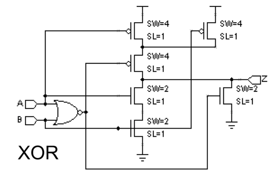
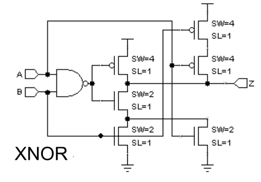
The NAND gate is just one of many possible gates that we will encounter in this course. We can make various logic gates: NAND, NOR, INV, XOR, etc using PFETs and NFETs and connecting them in a complementary way in order for them to work and produce the boolean logic as intended. The schematic of a XOR gate and an XNOR gate is as follows:
We will not test you on designing transistor-level circuitry, but you should be able to derive its truth table given the corresponding CMOS circuitry.
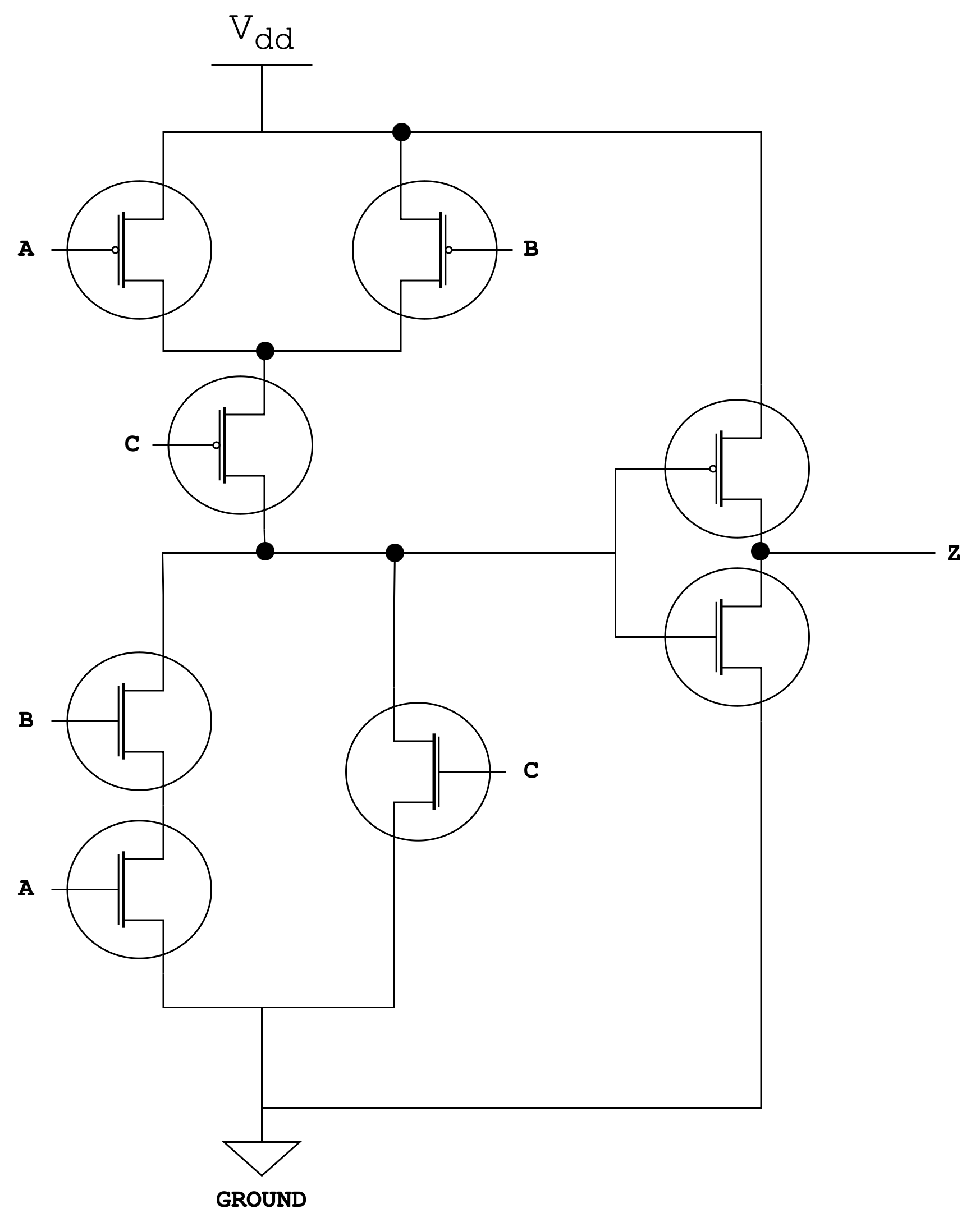
As an exercise, write down the truth table of the following CMOS circuitry:
Timing Specifications of Combinational Logic Devices
Propagation Delay and Contamination Delay are critical timing metrics in digital circuits. These delays exist due to the physical and electrical properties of the circuit components and are crucial for ensuring reliable operation.
Combinational devices must be documented with proper timing specifications that specify the upper bound (propagation delay) required to compute the specified output given a set of valid and stable input values, and the lower bound (contamination delay) before the output may begin to change after a change in the inputs.
Propagation Delay \(t_{pd}\)
Propagation Delay
Assume the output of a device is initially invalid. The propagation delay, denoted as \(t_{pd}\) is defined as the time taken for the device to produce a valid output, measured the moment it was given a valid input. It determines the maximum speed at which a circuit can operate.
To find the propagation delay of a circuit schematic, follow these steps:
- Identify All Paths: List all possible paths from any input to any output.
- Calculate Delay for Each Path: For each path, sum the propagation delays of all the gates along that path.
- Determine the Longest Path: Identify the path with the highest total delay, known as the critical path.
- Total Propagation Delay: The propagation delay of the circuit is the delay of the critical path.
Critical Path
The critical path in a digital circuit is the longest path from any input to any output, which determines the maximum propagation delay of the circuit.
It is the path that takes the most time for a signal to travel through the circuit, and it defines the overall speed at which the circuit can operate, as the circuit cannot produce a valid output (all bits) until all signals have propagated through this path.
The propagation delay is determined by the longest path because it dictates the maximum time the circuit takes to stabilize its output after an input change.
- Sequential dependency: Each component (gates, made up of FETS in CMOS arrangements) in the combinational logic circuit must wait for one another to produce a valid overall output.
- Overall output validity: All components must produce valid results before final output (the last logic gate in the circuit) can be produced.
For a device with more than one output bit, all output bits must be valid simultaneously for the device to function correctly. This means that the propagation delay of the device is determined by the longest delay among all the output paths, ensuring all outputs are stable and valid at the same time.
Contamination delay \(t_{cd}\)
Another timing specification that is typically measured an indicated on a combinational logic device is the contamination delay.
Contamination Delay
Assume the output of a device is initially valid. The contamination delay denoted as \(t_{cd}\) is defined as time taken for the device to produce an invalid output when it was initially valid, measured from the moment it was given an invalid input. This ensures that signals stabilize before propagating to the next stage in a circuit.
To find the contamination delay of a circuit schematic, follow these steps:
- Identify All Paths: List all possible paths from any input to any output.
- Calculate Delay for Each Path: For each path, sum the contamination delays (minimum delays) of all the gates along that path.
- Determine the Shortest Path: Identify the path with the lowest total contamination delay.
- Total Contamination Delay: The contamination delay of the circuit is the delay of the shortest path.
Shortest Path
The shortest path in the context of contamination delay is the path through the circuit that has the minimum total delay from an input to an output.
This path defines the contamination delay because it represents the fastest possible route for a signal to propagate through the circuit, indicating the earliest time at which any output may change (such as become invalid from previously being valid) in response to a change at the input.
The intuition behind why t\(_{cd}\) is calculated as the minimum cumulative contamination delay over all paths:
- Fastest propagation of errors: errors take the fastest route to propagate invalid signal and finally,
- Earliest contamination: errors contaminate ANY output (to be invalid, when it was initially valid) via this shortest path
For contamination delay, it is enough for just one output bit to become invalid for the entire device to be considered invalid. The contamination delay indicates how long the circuit can hold its previous valid output (all bits) before any invalid input starts to affect the output, representing the minimum time the circuit can maintain its state before any bit becomes invalid.
Exercise
Complementary pull-up (made up of PFETs) and pull-down circuits (made up of NFETs) form a CMOS gate. With these gates, we can form a combinational logic circuit, example as shown:

Given the \(t_{pd}\) and \(t_{cd}\) for the NAND gate: \(t_{pd} = 4 ns\), \(t_{cd}=1ns\), we can find that:
- The overall \(t_{pd}\) of the circuit is \(12 ns\) (the path in red)
- The overall \(t_{cd}\) of the circuit is \(2 ns\) (the path in blue)
Summary
You may want to watch the post lecture videos here.
Here are the key points from this notes
- MOSFETs Basics: NFETs and PFETs are both MOSFETs, they behave like switches. NFETs are activated by applying high voltage at the gate, and will produce low voltage at its drain. PFETs are activated by applying low voltage at the gate, thus producing high voltage at its drain.
- Complementary MOS: The use of complementary pairs of NFETs and PFETs are crucial to form stable and efficient logic gates. A parallel NFET circuit must have a complementary series PFET counterpart, and vice versa.
- Logic Gates: We were introduced with CMOS schematic of basic logic gates like NAND, NOR, XOR, and XNOR. We also must be able trace the functionality of a given CMOS circuit.
- Timing Specifications: Propagation delay (tpd) and contamination delay (tcd) exist due to the physical and electrical properties of combinational logic devices. To compute tpd, find the critical path through the circuit. To compute tcd, find the fastest path through the circuit.
Knowing how long the combinational device takes to react (at most) tells us how often (e.g: at what rate) can we supply new inputs to the device, and how fast the device can process/compute a batch of input values.
We can assemble a few FETs to implement any truth table or Boolean functions (we will learn this more in next chapter), hence creating combinational logic devices. A specific type of combinational logic devices that has one output bit is called as gate. There are many types of gates, depending on the Boolean function that’s realised. Then, an even larger combinational logic circuits (that realises more complicated Boolean functions) can be created by assembling many of these gates together. We will learn how to build more complex circuits in the next few chapters.
Appendix
Please refer to this section if you are interested to learn more about p-type and n-type semiconductors, PN junction, and source-drain terminal naming.
P-type and N-type Semiconductors
Not to be confused with PFET and NFET.
In the p-type semiconductor there are plenty of acceptor atoms and in the n-type semiconductor there are plenty of extra electrons (donor atoms). We can say that a p-type region is where the majority of the carriers are holes and an n-type region is where the majority of the carriers are electrons.
To be precise, an electron is one of the constituents of an atom, having a negative charge. An acceptor atom has for example 3 electrons in valence shell and can accept one electron to complete the covalent bonding. Thus it gains one extra electron and acquires negative charge. On the other hand, a donor atom has 5 electrons (one extra) in valence shell and can donate one extra electron. It thus acquires unit positive charge in the process.
Depletion Region
When p-type and n-type semiconductors are placed together, the free electrons from n-type will flow over (diffuse) to the p-type and fill its holes (impurities). Filling up a hole results in a negatively charged ion at the p-type semiconductor, as illustrated as the gray circles in Figure above. Equally, these free electrons leaving the n-type leaves behind a positively charged ion at the n-type semiconductor. This is illustrated as the yellow circles.
Eventually, a space-charge builds up forming an electric field as denoted in the left drawings (the yellow circles and the grey circles form electric field), preventing more free electrons from the n-type side to the p-type side, thereby forming an insulating layer called depletion region.
P-channel or N-channel Formation
For NFETs, when there’s presence of high (positive) voltage at the gate, it repels the extra holes at the p-type bulk. Basically, a positive voltage applied to the gate attracts electrons (which are minority in the p-type substrate) to the interface between the gate dielectric and the two n-types semiconductors (drain and source).
These electrons form a conducting n-type channel between the source and the drain, called the inversion layer. When there’s potential difference between the drain and the source, the current will flow from drain to source through this inversion layer.
For PFETs the opposite happens. When there’s presence of low (negative) voltage at the gate, it repels the extra electrons at the n-type bulk. Basically, holes (which are minority in the n-type substrate) are the majority in the region between the gate dielectric and the two p-types semiconductors, forming a conducting p-type channel (inversion layer). When there’s potential difference between drain and source, then the current will flow from source to drain through this inversion layer.
The position of the source and drain in PFET is switched , compared to what is depicted for NFET. Read the next section for details.
Naming of Source and Drain
The naming of the Source and Drain terminal depends on the majority of the charge carrier. The majority charge carrier is always meant to be drained at D and sourced at S, meaning that it flows from S to D.
In PFETs, current flows from Source to Drain, because the majority of the charge carrier is holes (positively charged). In NFETs, current flows from Drain to Source, because the majority of the charge carrier is electrons (negatively charged).
Current (I) cannot flow out back to the Gate because there’s a capacitor there (infinite resistance). The function of the gate capacitor is to create electric field enough to pull either electrons up to the gate in NFETS or holes up to gate in PFETs to create a conductive n-type (electrons) or p-type(holes) channel.
Reverse Bias in PN Junction
The bulk of the PFET is connected to the VDD while the bulk of the NFET is connected to the GND. We do this to keep the PN junction in each FET to stay in the reverse biased state by default, until they’re switched on. A simple explanation on why we need to keep them in reverse biased state by default is so that it encourages the presence of the depletion region hence preventing major current leaks across the junction when the FET is off. You may watch this video that we made if you’d like to know more about reverse biasness (and other stuffs like the PN junction diode, and P/N type semiconductors), but these details are out of our syllabus.