 50.002 CS
- Beta Assembler and Simulator
- How the Assembler Works
- Usage
- Assembly Syntax
- ISA Reference (beta_32.py)
LDandST- Tetris Board Simulator (
tetrisbranch) - Sample Test Program
- Summary
50.002 Computation Structures
Information Systems Technology and Design
Singapore University of Technology and Design
Beta Assembler and Simulator
Source Code
You can find the assembler source code on GitHub:
mainbranch (assembler + peg solitaire): github/natalieagus/beta-assembler (main)tetrisbranch (assembler + Tetris board simulator): github/natalieagus/beta-assembler (tetris)
Overview
This is a Python assembler and interactive step debugger for the MIT Beta ISA (32-bit). It translates .uasm assembly source files into binary or hex byte arrays suitable for loading onto the Alchitry AU FPGA via Lucid’s $readmemh. The assembler was originally written by Alex, a 2024 CSD graduate. The simulator and Tetris board renderer were added on top of his assembler pipeline.
Requirements
Python 3.10 or later. Install dependencies with:
pip install parameterized
The curses-based simulators work on macOS and Linux terminals out of the box. On Windows, use WSL.
Project Structure
beta-assembler/
├── assembler.py          # Core assembler: .uasm source -> binary/hex byte lists
├── assembler_wrapper.py  # CLI wrapper around assembler.py
├── beta_32.py            # Beta ISA definition: instruction encoders, register names
├── helper_functions.py   # Number parsing, two's complement, hex/bin conversion
├── shunting_yard.py      # Expression evaluator (handles labels, arithmetic in .uasm)
└── files/
    ├── game.uasm         # Peg solitaire game instruction memory
    ├── game_data.uasm    # Peg solitaire game data memory
    └── test*.uasm        # Various test programs
How the Assembler Works
Input Files
Instruction and data memory are kept in separate files:
filename.uasm: instruction memoryfilename_data.uasm: data memory (optional)
Labels defined in data memory are passed to the instruction assembler so they can be referenced in LD, ST, and branch instructions.
Two-Pass Assembly
The assembler runs two passes over the source:
- First pass: resolves all label addresses and symbolic constant assignments by executing each instruction with dummy arguments. This populates the label table with correct byte addresses.
- Second pass: emits the final encoding using the resolved label values.
Output Format
The hex/bin dump is written in reverse address order (lowest address at the bottom of the file). This matches the Lucid memory initialisation format expected on the Alchitry AU.
If you are using Verilog’s $readmemh, you do not have to reverse it and you should not have trailing ,. Change the implementation of arr_to_str in assembler.py:
        if input_format == "data":
            return "\n".join(
                [
                    f"{output_prefix}{''.join(data[i : min(i + (beta.memory_width // 8), len(data))][::-1])},"
                    for i in range(0, len(data), (beta.memory_width // 8))
                ][::-1] # reverses
            )
        else:
            return "\n".join(
                [
                    f"{output_prefix}{''.join(data[i : min(i + (beta.instruction_width // 8), len(data))][::-1])},"
                    for i in range(0, len(data), (beta.instruction_width // 8))
                ][::-1] # reverses
            )
You also need to strip the h header by changing the output_formatter:
output_formatter = {
    "bin": (bin, 8, "b"),
    "hex": (hex, 2, "h"),
}
Usage
Assembling a Program
cd beta-assembler
python assembler_wrapper.py files/game -b    # binary output
python assembler_wrapper.py files/game -x    # hex output
Output files are written alongside the input:
files/game.bin  or  files/game.hex         # assembled instruction memory
files/game_data.bin  or  files/game_data.hex    # assembled data memory
CLI Options
| Flag | Description |
|---|---|
-b, --bin |
Output in binary format (default) |
-x, --hex |
Output in hexadecimal format |
-s, --silent |
Disable printing to console |
-o filename, --out filename |
Specify output filename (defaults to input name) |
Assembly Syntax
Comments, Labels, and Constants
| This is a comment (everything after | on a line is ignored)

delay = 1              | Symbolic constant assignment

. = 0x2600             | Set current address (dot)

TETRIS_BOARD:          | Label (must be on its OWN line)
LONG(0)                | 32-bit word
WORD(0)                | 16-bit word
Labels must be placed on their own line. A label followed immediately by an instruction on the same line will not be parsed correctly.
Example Instructions
CMOVE(1, R1)               | Constant-move: R1 = 1
ADDC(R1, 5, R2)            | R2 = R1 + 5
ST(R1, TETRIS_BOARD, R2)   | mem[TETRIS_BOARD + R2] = R1
LD(R31, x, R1)             | R1 = mem[x + R31]
BEQ(R0, my_label, R31)     | branch if R0 == 0
BR(loop)                   | unconditional branch
HALT()                     | stop execution
Data Directives
| Directive | Description |
|---|---|
WORD(val) |
Assemble val as a 16-bit datum |
LONG(val) |
Assemble val as a 32-bit datum |
STORAGE(N) |
Reserve N 32-bit words of memory |
ISA Reference (beta_32.py)
The ISA is defined in beta_32.py as Python lambda functions. All instruction encoders return a list of 8-character binary strings (one per byte, little-endian).
Key Parameters
| Parameter | Value |
|---|---|
instruction_width |
32 bits |
memory_width |
32 bits |
output_size |
2 hex chars per byte |
Instruction Format (32 bits)
Type 1 (register):
[31:26] opcode   [25:21] RC   [20:16] RA   [15:11] RB   [10:0] unused

Type 2 (literal):
[31:26] opcode   [25:21] RC   [20:16] RA   [15:0] CC (signed 16-bit constant)
The destination register is always last in the assembly syntax (e.g., ADD(RA, RB, RC) stores the result in RC).
Register Aliases
| Name | Number | Role |
|---|---|---|
| BP | R27 | Base/frame pointer |
| LP | R28 | Link register (return address) |
| SP | R29 | Stack pointer |
| XP | R30 | Interrupt return pointer |
| R31 | R31 | Always zero (hardwired) |
Instruction Set Summary
| Category | Instructions |
|---|---|
| Arithmetic | ADD, ADDC, SUB, SUBC, MUL, MULC, DIV, DIVC |
| Logic | AND, ANDC, OR, ORC, XOR, XORC, XNOR, XNORC |
| Shift | SHL, SHLC, SHR, SHRC, SRA, SRAC |
| Compare | CMPEQ, CMPEQC, CMPLE, CMPLEC, CMPLT, CMPLTC |
| Branch | BEQ/BF, BNE/BT, BR, JMP |
| Memory | LD, ST, LDR |
| Pseudo | MOVE, CMOVE, PUSH, POP, CALL, RTN, XRTN |
| Data | WORD, LONG, STORAGE |
| System | HALT(), SVC(code), RAND, NOP |
Non-Standard Extensions
RAND (opcode 0x03) and NOP (opcode 0x02) are custom extensions, not part of the original MIT Beta ISA. Your FPGA datapath must implement support for these opcodes if your program uses them. Modify the opcodes in beta_32.py as needed for your own design.
System Call
SVC(code) has opcode 0x01. The code argument is embedded in the 16-bit constant field. The datapath is responsible for handling the trap.
LD and ST
By default, we make LD a 2-cycle instruction (assembled twice), so that it covers 2 CPU cycles because BRAM needs synchronous reads. However, ST is sufficient in a single-cycle. We write down 3 possible scenarios below.
Clock Definitions
Suppose you have varying clock speed for CPU and the BRAM:
- clkB: the CPU clock.
- clkA: twice the frequency of clkB. Generated from the same MMCM with a 180 degree phase offset, so clkA rising edges fall midway between clkB edges.
Timing Reference
All times are relative to a rising edge of clkB, called t. Let T be one quarter of the clkB period (equivalently, one half of the clkA period).
| Label | Offset | Event |
|---|---|---|
t |
0 | Rising edge of clkB |
t+T |
+T | First rising edge of clkA after t |
t+2T |
+2T | Falling edge of clkB |
t+3T |
+3T | Second rising edge of clkA after t |
t+4T |
+4T | Next rising edge of clkB (start of next CPU cycle) |
Here’s a simple illustration with clkA = 25Mhz, and clkB = 50Mhz.

Common Assumptions
- Instruction memory and data memory are separate (Harvard style).
- PC has a combinational read port and a synchronous write port.
- Register file has combinational read ports and a synchronous write port.
- The data BRAM is simple dual-port: one read port and one write port. This BRAM makes up Instruction and Data memory.
- The write port of the data BRAM is always owned by the CPU (never shared with the GPU).
- In scenarios where the GPU shares the data BRAM, only the read port is time-multiplexed, not the write port.
Scenario 1: BRAM Clocked at clkB (Same Speed as CPU), Unshared
Clock setup:
- Instruction BRAM: posedge clkB
- Data BRAM: posedge clkB
- PC: posedge clkB
- Regfile: posedge clkB
clkA is not used and everything runs on a single clkB.
LD: Must be 2 Cycles
- At
t, posedge clkB fires. PC presents the instruction address. The instruction BRAM latches this address and, shortly after, outputs the instruction. Suppose it isLD. - Combinational logic decodes the instruction, reads registers, and the ALU computes the effective address (EA). All of this settles some time after
t. - The data BRAM also clocks on posedge clkB. It already latched whatever was on its address input at
t, which was not theEA(theEAdid not exist yet). The data BRAM’s one and only edge this cycle has already passed. - At
t+4T, the next posedge clkB fires. The data BRAM can now latch theEA. But the regfile also latches att+4T. The BRAM output (Mem[EA]) only stabilizes aftert+4T, so the regfile cannot capture it at this edge. - The regfile should capture
Mem[EA]att+8T(the next posedge clkB). LD takes 2 cycles. - During
t+4Ttot+8T, the instruction cannot change.
With only one BRAM edge per CPU cycle, the EA cannot be both computed from the instruction and presented to the data BRAM within the same cycle. The read output then arrives too late for the regfile to latch.
ST: 1 Cycle
- At
t, the instruction BRAM outputsST. Combinational decode, reg read, and ALU produce both the EA and the store data (Reg[Rc]). Both are stable well beforet+4T. - At
t+4T, posedge clkB fires. The data BRAM write port latches EA and Reg[Rc], and the write commits. - No regfile writeback is needed (WERF=0 for ST).
ST only needs the BRAM write port, and the write inputs (EA and data) just need to be stable before the next edge. Unlike LD, there is no BRAM read output that must propagate back to the regfile.
Scenario 2: BRAM Clocked at clkA (2x CPU Speed), Unshared
Clock setup:
- Instruction BRAM: posedge clkA
- Data BRAM: posedge clkA
- PC: posedge clkB
- Regfile: posedge clkB
The 2x clock gives BRAMs two edges per CPU cycle: t+T and t+3T.
LD: 1 Cycle is Enough
- At
t, posedge clkB fires. PC advances and presents the new instruction address. - At
t+T, posedge clkA fires. The instruction BRAM latches the address and shortly after outputs the instruction (LD). - Combinational decode, reg read, ALU computes
EA. This settles betweent+Tandt+3T. - At
t+3T, posedge clkA fires again. The data BRAM latches theEA. - Shortly after
t+3T, the data BRAM outputsMem[EA]. - At
t+4T, posedge clkB fires. The regfile latchesMem[EA]into the destination register. PC advances. Done in 1 cycle.
The 2x clock provides a second BRAM edge (t+3T) between the moment the instruction appears (t+T) and the moment the regfile latches (t+4T). This is exactly the extra edge needed to service the data BRAM read.
ST: 1 Cycle
- Instruction appears after
t+T. Decode, reg read, ALU produce EA and Reg[Rc] beforet+3T. - At
t+3T, the data BRAM write port latches EA and Reg[Rc]. Write commits. - No regfile writeback needed.
Scenario 3: BRAM Clocked at clkA (2x CPU Speed), Read Port Shared with GPU
Clock setup:
- Instruction BRAM: posedge clkA
- Data BRAM: posedge clkA, but the read port is time-multiplexed:
ttot+2T(first clkA half): CPU’s read slot (latches att+T)t+2Ttot+4T(second clkA half): GPU’s read slot (latches att+3T)
- Data BRAM write port: CPU only, not shared
- PC: posedge clkB
- Regfile: negedge clkB (at
t+2T), because the posedge-to-posedge window crosses into GPU territory
The regfile latches on negedge clkB (t+2T) instead of posedge because the second half of each clkB period (t+2T to t+4T) is the GPU’s read slot. For non-memory ALU instructions, the result is ready before t+2T, so latching at negedge works. This setup is discussed in this page too.
LD: Must be 2 Cycles
- At
t, posedge clkB fires. PC presents the instruction address. - At
t+T, posedge clkA fires (CPU’s read slot). The instruction BRAM latches the address and shortly after outputs the instruction (LD). Simultaneously, the data BRAM read port latches whatever address the CPU is presenting.- But the correct
EAdepends on the instruction that is only now appearing. - The CPU cannot have a valid
EAready att+T. - Combinational decode, reg read, ALU compute
EAis only possible after instruciton is received att+T.
- But the correct
- At
t+2T, negedge clkB fires. The regfile latches. But the data BRAM never received the correctEAthis cycle, so there is correctMem[EA]to write back. - At
t+3T, posedge clkA fires, but this is the GPU’s read slot. The CPU cannot use the data BRAM read port, unless it is somehow cached. We assume no cache. - The pipeline stalls. PC does not advance at
t+4T. The LD’s control signals are held. - At
t+5T(next CPU read slot), posedge clkA fires. The data BRAM read port latches theEA. - Shortly after
t+5T,Mem[EA]appears on the data output. - At
t+6T(negedge clkB of the next cycle), the regfile latchesMem[EA]into the destination register. LD completes after 2 cycles.
The CPU’s single data BRAM read slot (t+T) coincides with the instruction BRAM output. The EA depends on the instruction, so it cannot be ready at the same edge that produces the instruction. The GPU’s ownership of the t+3T read slot eliminates the fallback that makes Scenario 2 work.
ST: 1 Cycle
- At
t+T, instruction BRAM outputsST. Decode, reg read, ALU produce EA and Reg[Rc]. Both settle beforet+3T. - At
t+3T, the data BRAM write port (CPU-only, no GPU contention) latches EA and Reg[Rc]. Write commits. - No regfile writeback needed.
The GPU shares the read port, not the write port. ST only needs the write port, so GPU contention is irrelevant.
Summary of Clock Cases
| Instruction | Scenario 1 (clkB, unshared) | Scenario 2 (clkA, unshared) | Scenario 3 (clkA, shared reads) |
|---|---|---|---|
| LD | 2 cycles | 1 cycle | 2 cycles |
| ST | 1 cycle | 1 cycle | 1 cycle |
LD is the only instruction affected because it is the only one that requires a data BRAM read whose output must feed back into the regfile within the same cycle. ST avoids this because it only writes to the BRAM and does not need the result to propagate anywhere.
We do not discuss this phenomenon in detail while learning Beta CPU in class because we assume that the RAM has combinational read ports, therefore instruction read and data read from the RAM can happen all in the same cycle.
Tetris Board Simulator (tetris branch)
The Tetris simulator is available on the tetris branch. Switch to it with git checkout tetris.
Running the Simulator
cd beta-assembler
python sim_tetris.py files/tetris
This assembles and executes files/tetris.uasm + files/tetris_data.uasm, rendering the board stored at the TETRIS_BOARD data label in real time.
Board Layout
The board is a 22 rows x 12 columns grid. Each cell is one LONG (4 bytes, 32-bit little-endian) in data memory. Cell (row, col) is at byte address:
TETRIS_BOARD + (row * 12 + col) * 4
Column 0 and column 11 are permanent walls, pre-filled with 1 in tetris_data.uasm. A cell value of 1 renders as [] (green); 0 renders as empty; walls render as ## (yellow).
Display
The terminal display shows the board on the left (27 terminal columns wide), all 32 registers on the right, and disassembly below showing the current PC and any breakpoints.
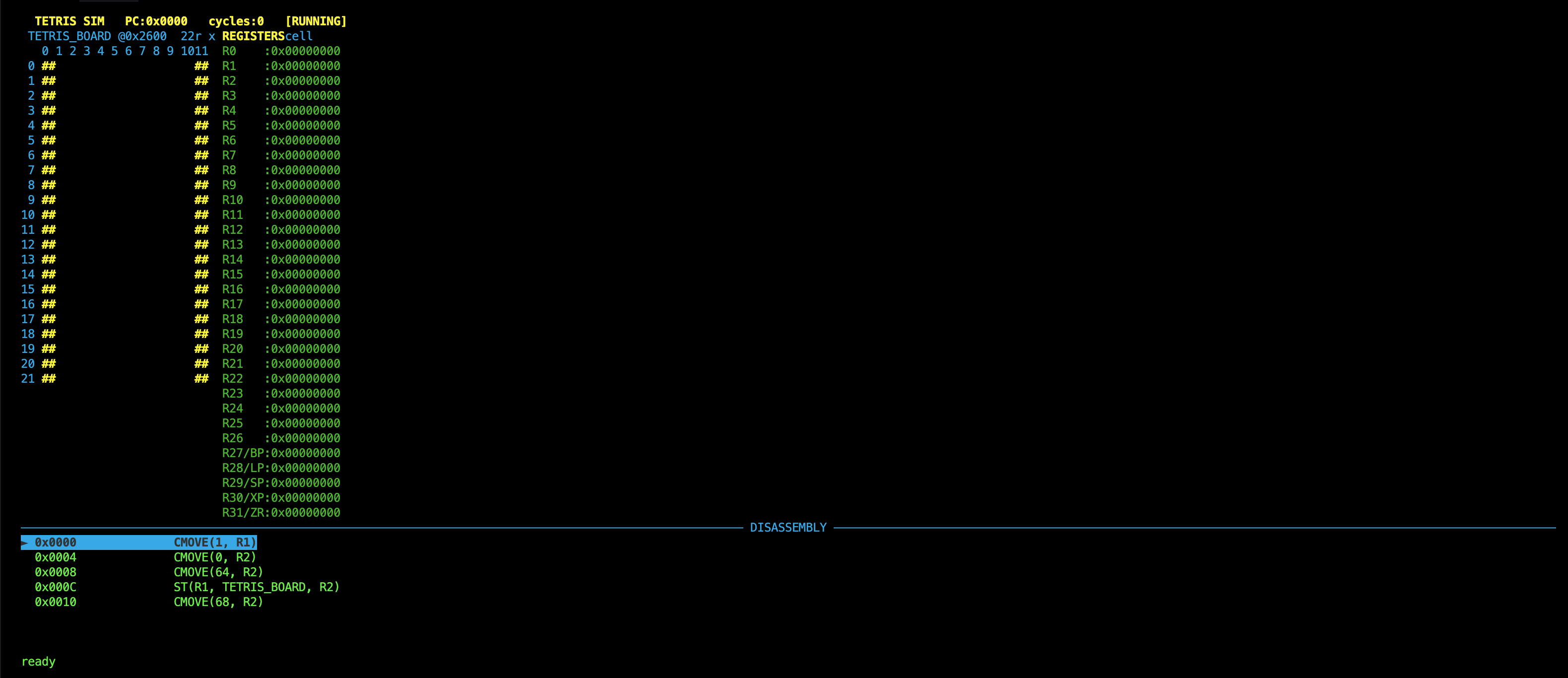
Keyboard Controls
| Key | Action |
|---|---|
n |
Step one instruction |
r |
Run until breakpoint or HALT |
b |
Toggle breakpoint at current PC |
c |
Clear all breakpoints |
R |
Reset: PC back to 0, board restored to initial state |
q |
Quit |
How the Simulator Uses the Assembler
sim_tetris.py calls parse_asm_file() from assembler.py directly. The .uasm source is assembled into a list of binary byte strings, which are then reconstructed into 32-bit instruction words and loaded into the simulator’s instruction memory. The simulator executes those words as machine code. Opcodes are resolved at runtime by encoding a dummy instruction for each operation using beta_32.py and extracting the 6-bit opcode field, so the simulator stays in sync with the ISA definition automatically.
Sample Test Program
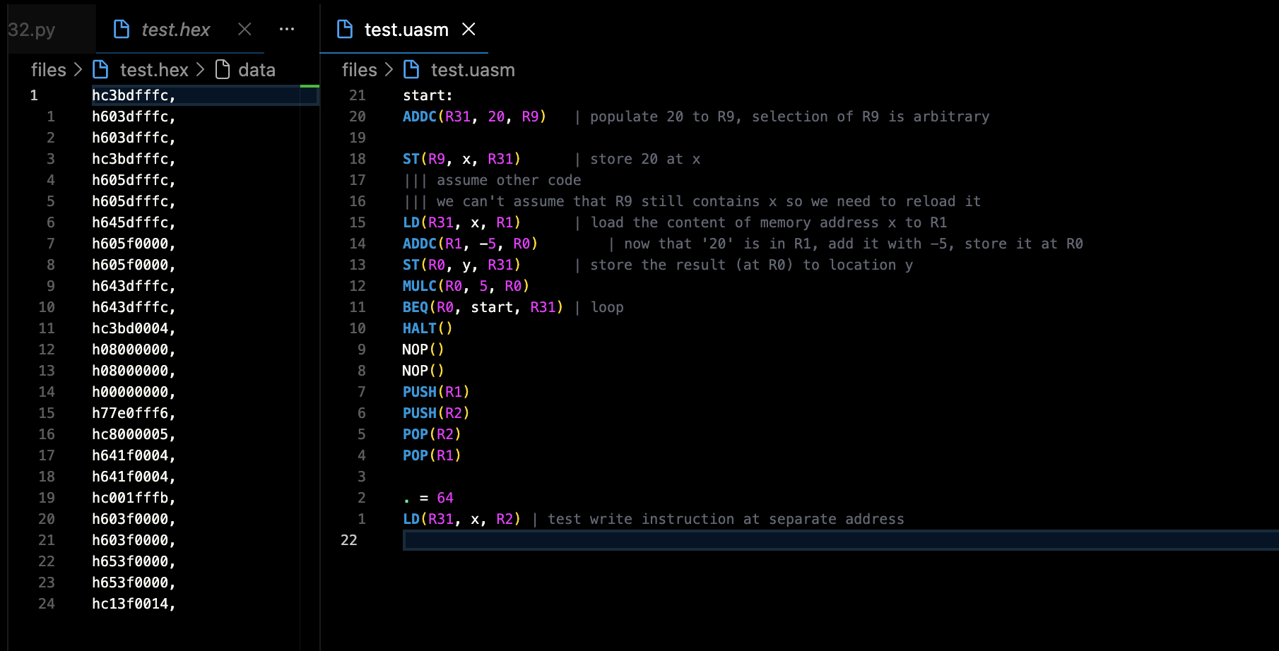
Here is a minimal example (files/test.uasm and files/test_data.uasm) that demonstrates loads, stores, arithmetic, and branching.
Instruction memory (test.uasm):
start:
ADDC(R31, 20, R9)       | populate 20 to R9

ST(R9, x, R31)          | store 20 at label x
LD(R31, x, R1)          | load content at x into R1
ADDC(R1, -5, R0)        | R0 = R1 + (-5) = 15
ST(R0, y, R31)          | store result at label y
MULC(R0, 5, R0)
BEQ(R0, start, R31)     | loop back to start
HALT()
Data memory (test_data.uasm):
x:
LONG(0)                  | label x points here
y:
LONG(0)                  | label y points here
Assemble with:
python assembler_wrapper.py files/test -x
Summary
- The hex output is reversed relative to address order to match Lucid’s
$readmemhformat on the Alchitry AU. beta_32.pyis the authoritative ISA definition. Do NOT hardcode opcode values anywhere else. Always derive them frombeta_32by encoding a test instruction and reading back the opcode field.- Labels must always be placed on their own line. A label followed by an instruction on the same line will not be parsed correctly.