 50.002 CS
- Starter Code and Tools
- Related Class Materials
- Exploring Logic Gates
- Voltage Specification and Noise Immunity
- Summary
- Appendix
50.002 Computation Structures
Information Systems Technology and Design
Singapore University of Technology and Design
Lab 0: Digital Abstraction
Starter Code and Tools
We will be using MIT’s JSim for this lab, a circuit simulation program useful to study the theoretical behaviour of various logic gates and digital circuits.
Clone the starter code from here:
git clone https://github.com/natalieagus/jsim-kit.git
JSim uses mathematical models of circuit elements to make predictions of how a circuit will behave both statically (DC analysis) and dynamically (transient analysis). We will not be learning how to use JSim or write JSim netlists. If you’re interested in JSim syntax and how it works, head to appendix section.
You will need Java to run JSim. You should already have it installed for 50.001.
Open JSim
Open JSim and you should see the following user interface:
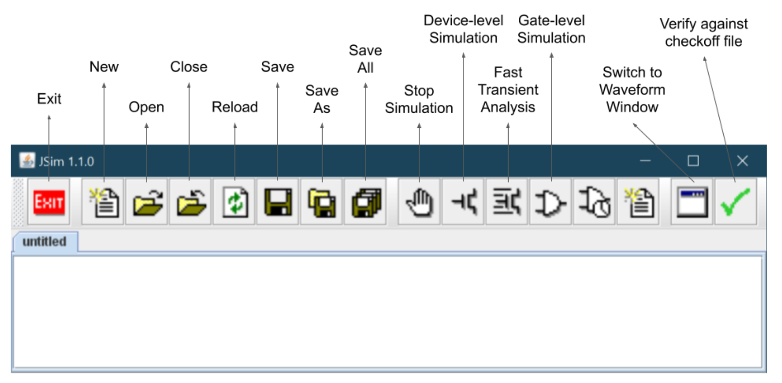
Your job now is to simply Open the right .jsim netlist file for each Task of this Lab, and then run the simulation by clicking the Gate-level Simulation button (Task 1-3), or the Device-level Simulation button (Task 4-5).
Related Class Materials
The lecture notes on Basics of Information and Digital Abstraction are closely related to this lab.
Task 1 - Task 3: studying the graphical output of AND, OR, and XOR gates.
Related Notes: Basics of Information
Task 4 and Task 5: finding an optimal VTC
Related Notes: Digital Abstraction
- VTC Section
- Voltage Specifications and Noise Margin
- Realise that we can optimise the noise margin by optimising the MOSFET material
- Understand why
Exploring Logic Gates
Logic Gate
A logic gate is a basic building block used in digital circuits. It’s a device that performs a logical operation on one or more binary inputs to produce a single binary output.
These gates implement the basic operations of Boolean algebra, which underpins the functioning of computers and many other types of digital devices.
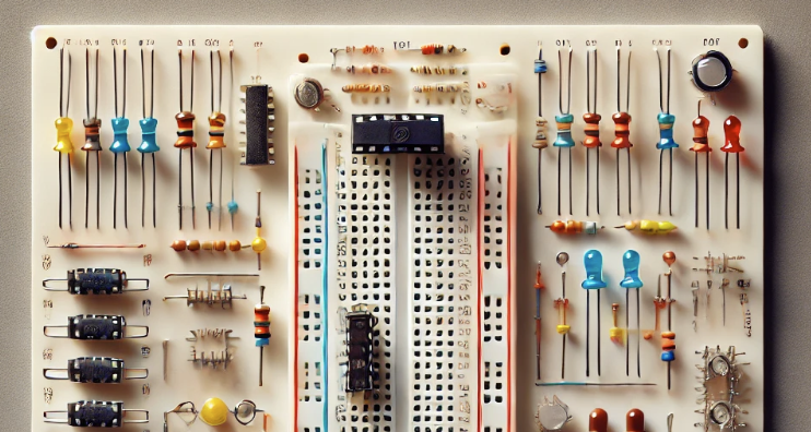
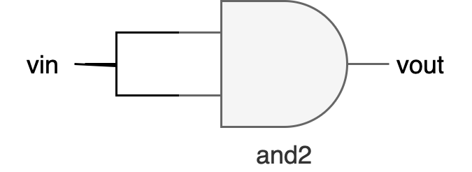
You can buy these gates for DIY projects and assemble them on a breadboard to make your own mini digital circuit:
We will now use JSim to simulate the behavior of AND, OR, and XOR logic gates, exploring their waveform outputs to better understand how they work theoretically.
Task 1: Generate AND Gate Waveform
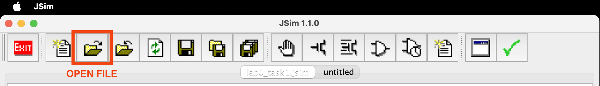
Open lab0_task1_to_3.jsim by clicking this button:
.include "nominal.jsim"
.include "8clocks.jsim"
.include "stdcell.jsim"

Xdriver1 clk1 a inverter
Xdriver2 clk2 b inverter
Xtest a b z and2

.tran 20ns

.plot a
.plot b
.plot z
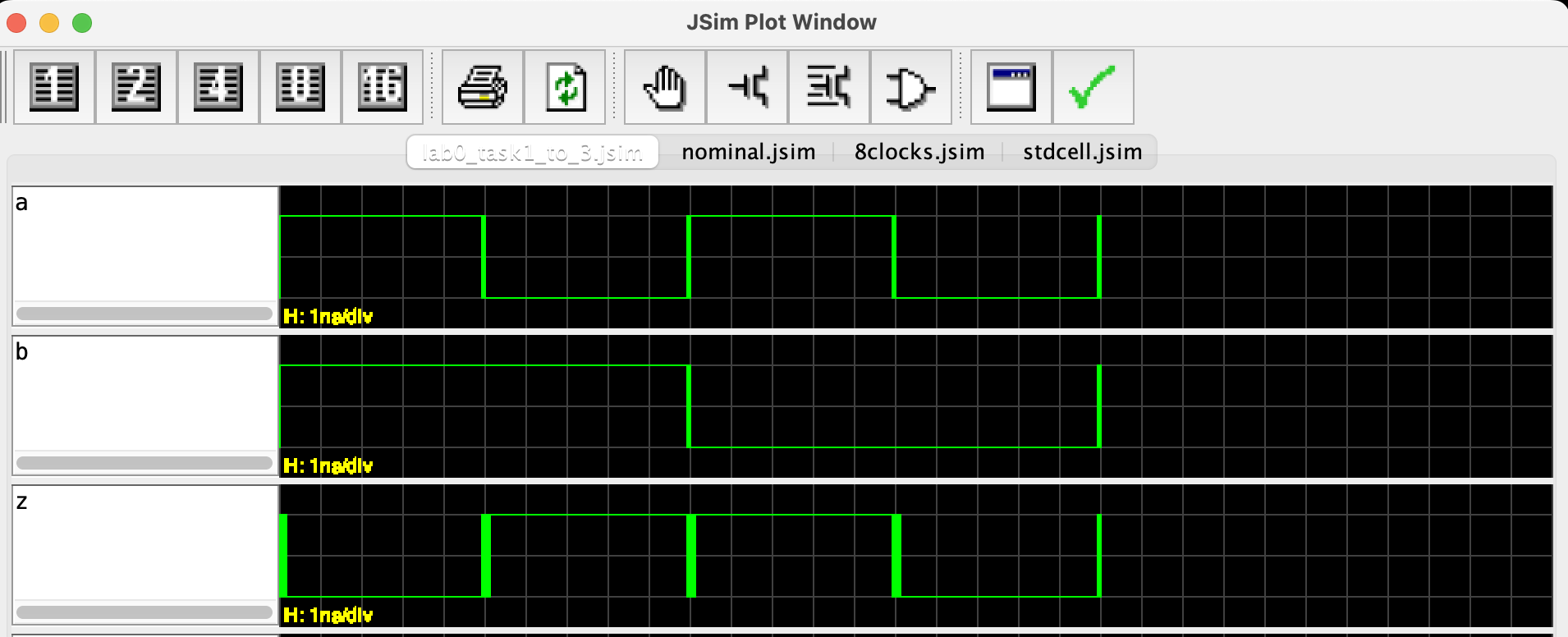
The netlist above describes this circuit setup:
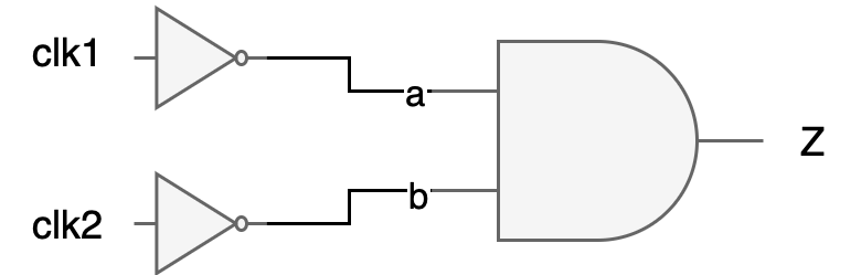
Here we use a square wave signal called clk1 (period of 10 ns) and clk2 (period of 20 ns) as inputs to each inverter called driver1 and driver2. We then connect each inverter to an AND gate.
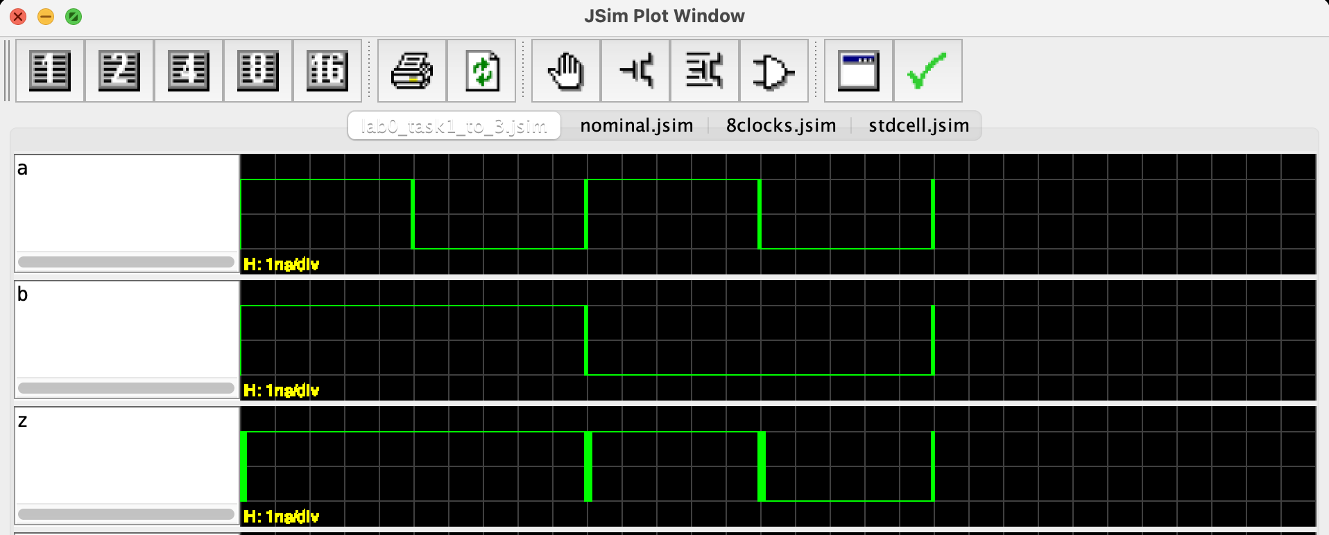
The line .tran 20ns means to simulate the circuit for 20ns. Finally, we see the plots of signals a,b,z. You can begin simulation by clicking the gate-level simulation button, then a waveform plot window will pop out as follows:
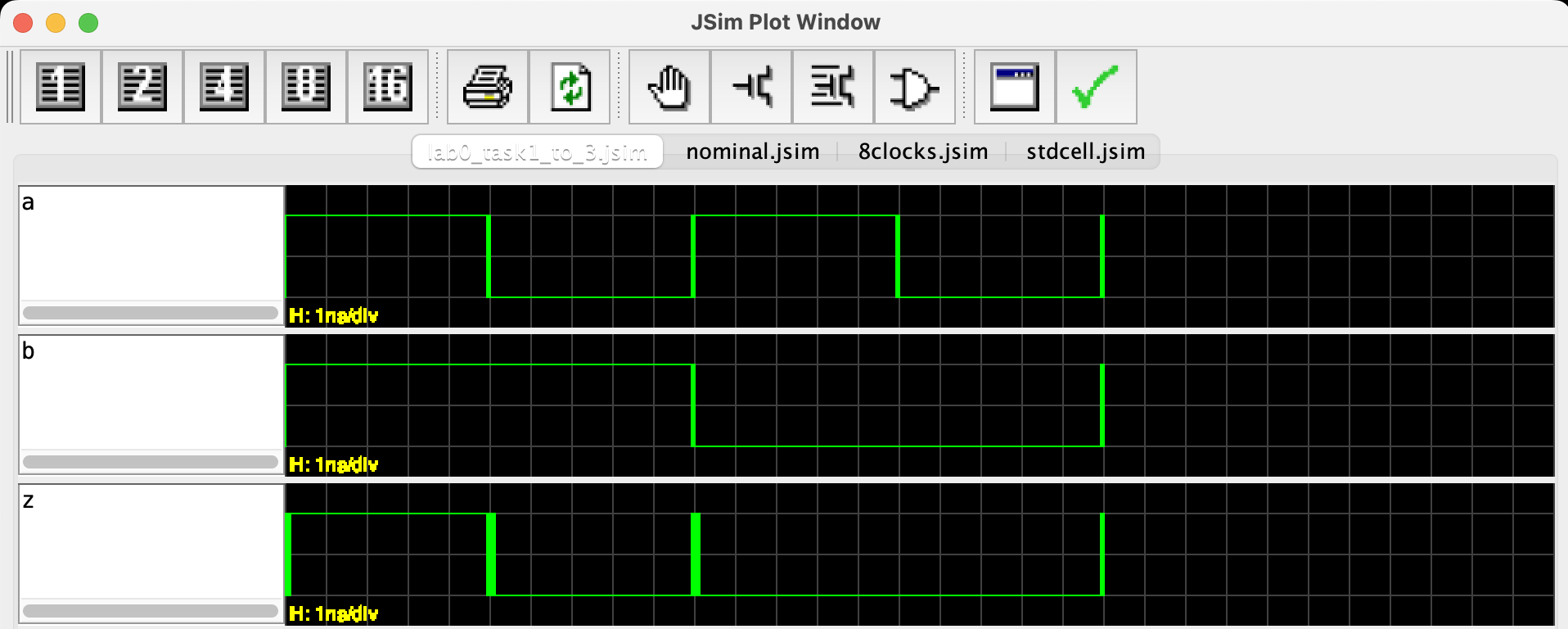
There are 3 plots in total:
- Each x-axis signifies time (from 0 to 20ns)
- Each y-axis signifies voltage value (analog values)
The z plot essentially illustrates the truth table (logic specification) of the AND gate.
Each waveform plot has an oscilloscope like grid in the background. You can use keyboard shortcut x to zoom out, X to zoom in, and c to reset. Use the slider to scroll to the time you want.
Head to edimension to answer some questions about this task.
Task 2: Generate OR Gate Waveform
Modify the netlist above to generate plot of OR gate by replacing and2 with or2. These gate names are defined within the library file: stdcell.jsim.
You should get the following waveform now:
Head to edimension to answer some questions about this task.
Task 3: Generate XOR Gate Waveform
Finally, replace or2 with xor2 to obtain the following waveform:
Head to edimension to answer some questions about this task.
Interpreting Analog Values as Digital Logic Values
The goal of Task 1-3 is to condition you with waveform plots (y-axis signifies voltage value, and x-axis signifies time). These voltage values can then be converted into digital values if it meets certain threshold:
- If
zis larger thanVoh, then it signifies digital value1 - Conversely, if
zis smaller thanVol, then it signifies digital value0 - If
aorbis larger thanVih, then they signify digital value1 - Conversely, if
aorbis smaller thanVil, then they signify digital value0
JSim can automatically convert these analog values into digital values in the plots using .plot L(a) instead of just .plot a.
.include "nominal.jsim"
.include "8clocks.jsim"
.include "stdcell.jsim"

Xdriver1 clk1 a inverter
Xdriver2 clk2 b inverter
Xtest a b z and2

.tran 20ns

.plot L(a)
.plot L(b)
.plot L(z)
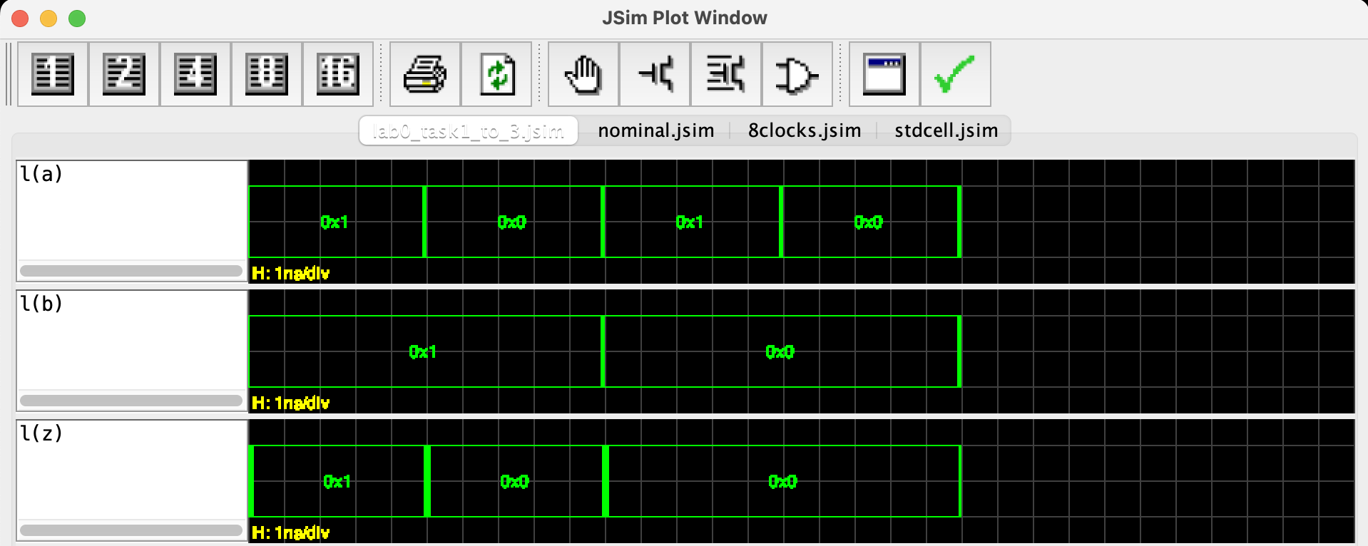
The logic thresholds (voltage specifications) are defined in nominal.jsim.
Undefined Logic Level
Zoom in and notice that there are some regions of undefined logic values (thick green lines):
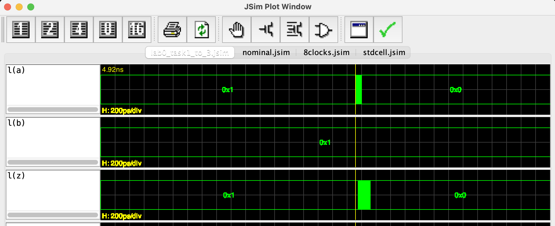
This simply means that the voltage value of the signals e.g: a or z during that time period is within the invalid voltage zone.
Can you guess what might have caused these artefacts? (you will have a concrete answer during next week’s lecture).
Voltage Specification and Noise Immunity
The goal of this section is to plot, study, and optimize the Voltage Transfer Characteristic (VTC) of the AND gate, allowing us to determine optimal voltage specifications (VOL, VOH, VIL, and VIH) for our digital circuits.
⚠️ Important
These four voltage specifications (also known as thresholds) are crucial because they ensure reliable operation across a combinational system composed of hundreds of gates, each of which must adhere to these standards to function correctly.
They are also critical for enhancing noise immunity in digital circuits by defining clear margins between logical high and low states, thereby reducing the likelihood of misinterpreting signals due to electrical noise.
Task 4: Optimising Noise Margins
Open lab0_task4_and_5.jsim. We give you the following netlist:
.include "nominal.jsim"
.include "custom_gates.jsim"

* dc analysis to create VTC
Xtest vin vin vout and2
Vin vin 0 0v

Vol vol 0 0.3v
Voh voh 0 3v

.dc Vin 0 3.3 .005
.plot vin vout voh vol
This is equivalent to this configuration:
To determine the VTC for and2, we’ll perform a dc analysis to plot the gate’s output voltage (vout) as a function of the input voltage (vin). Click the “Device level simulation” button, and you should see a new waveform window:

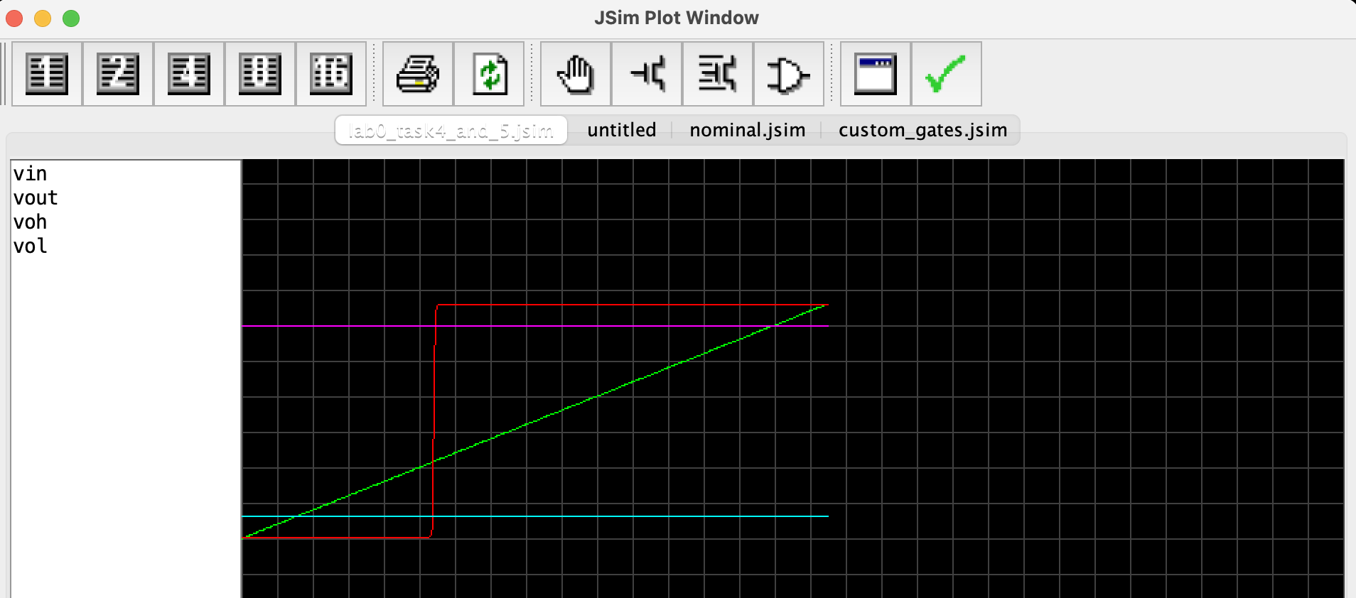
There are 2 helper lines:
- Top horizontal line: Voh (valid output high), set at 3V, which is 90% of the max operating voltage at 3.3V
- Bottom horizontal line: Vol (valid output low), set at 0.3V, which is 10% of the min operating voltage at 0V
The ‘S’ shape curve is the VTC of the and2 gate (vout), and the diagonal line is the plot of input voltage (vin). Notice how the VTC curve goes towards the left (not centered).
Since this is an AND gate, low vin will produce low vout and vice versa
In practice, before we manufacture these logic gates, we need to determine its physical dimensions that will give an optimum noise margin.
Centering the VTC
The optimum noise margin is present when the VTC of the device is centered between the minimum and the maximum operating voltage of the device.
Centered: The midpoint of the VTC curve should ideally align with the average of these two voltage limits.
By ensuring that the VTC is centered, you achieve a balance that allows the device to more effectively reject or tolerate noise within the circuit, thus increasing the reliability of detecting correct logic levels under varying electrical conditions.
The internal hardware implementation of the and2 gate is inside the file custom_gates.jsim. We will learn how to make these gates next week. But for now, all you need to know is that each gate is made up of another electronic components called transistors. We arrange these transistors in a specific way so that we can produce a logic gate with certain logic behavior, e.g: the nand gate.
We can vary the size of each transistors making up each gate (the sw and sl dimension, which refers to width and length of the transistors). This will directly affect the VTC plot of the and2 gate. You will learn more about the anatomy of the transistors (called MOSFET) next week, but head to appendix if you’re interested to find out more right now.
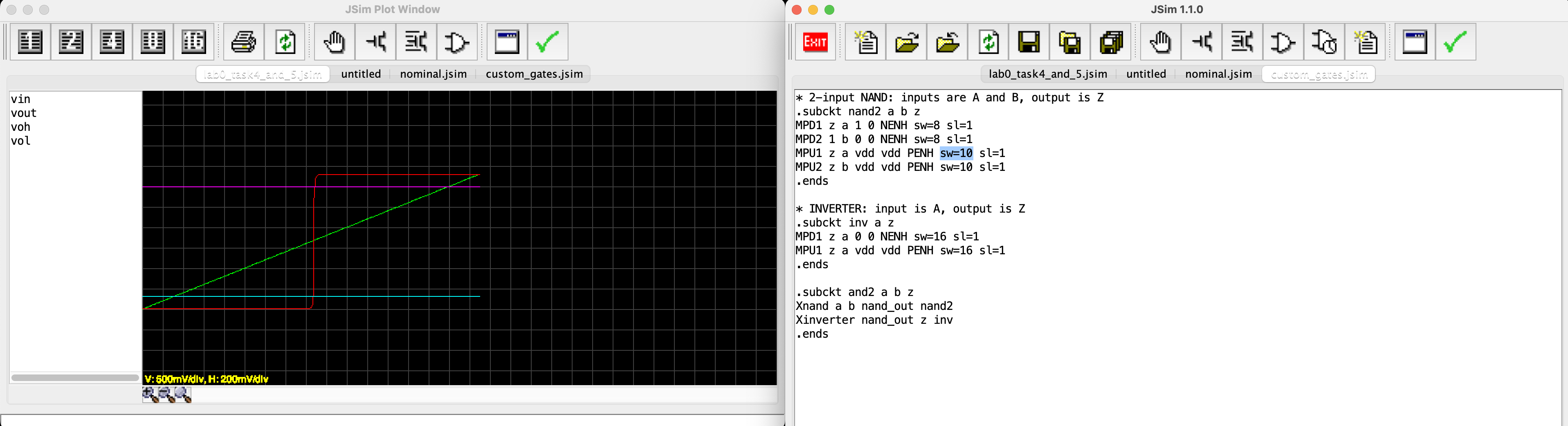
For instance, set the value of sw of MPU1 and MPU2 to be 10. Then, observe the change in the VTC output (click Device level simulation button again while focusing on lab0_task4_and_5.jsim pane). We now have a more centered VTC:
Head to edimension to answer some questions about this task.
VTC Characteristics vs. Switching Speed
The steepness of the VTC curve primarily indicates the static behavior of the gate and how sensitively the output voltage (Vout) responds to changes in the input voltage (Vin), and not directly imply dynamic characteristics of the gate such as the switching speed (e.g: how fast will we obtain a Vout given a Vin)
Task 5: Finding Noise Immunity of Centered VTC
Set the content of custom_gates.jsim to the following values to center the VTC:
* 2-input NAND: inputs are A and B, output is Z
.subckt nand2 a b z
MPD1 z a 1 0 NENH sw=8 sl=1
MPD2 1 b 0 0 NENH sw=8 sl=1
MPU1 z a vdd vdd PENH sw=10 sl=1
MPU2 z b vdd vdd PENH sw=10 sl=1
.ends

* INVERTER: input is A, output is Z
.subckt inv a z
MPD1 z a 0 0 NENH sw=16 sl=1
MPU1 z a vdd vdd PENH sw=16 sl=1
.ends

.subckt and2 a b z
Xnand a b nand_out nand2
Xinverter nand_out z inv
.ends
Since Voh and Vol is given (based on max and min operating voltage of the device), we need to find Vil and Vih from the graph. What do you think these values should be? (look back at your lecture notes).
The noise immunity of a gate is the smaller of the low noise margin (Vil - Vol) and the high noise margin (Voh - Vih).
- If we specify Vol = 0.3V and Voh = 3.0V, what is the largest possible noise immunity we could specify?
- If we specify Vol = 0.5V and Voh = 2.5V, what is the largest possible noise immunity we could specify?
Head to edimension to answer some questions about this task.
Summary
In Task 1-3, we examined the behaviors of AND, OR, and XOR gates using JSim so that we can understand their operations through waveform outputs.
In Task 4-5, we focused on optimizing the Voltage Transfer Characteristic (VTC) of an AND gate to define ideal voltage specifications (VOL, VOH, VIL, and VIH). This optimization is crucial for ensuring reliable circuit performance across systems comprising numerous gates and enhancing noise immunity.
Enhancing noise immunity is critical for maintaining signal integrity against electrical noise.
In practice, when designing complex combinational circuits that utilize multiple logic gates, optimizing the VTC of each gate is essential. This process ensures that the circuit as a whole operates reliably and efficiently.
Here’s how it works:
-
Optimize Each Gate: Each type of logic gate in the circuit—AND, OR, XOR, etc.—has its VTC optimized individually. This means adjusting parameters such as transistor sizes and arrangement within the gate to achieve the desired response curve, which determines how the gate transitions between its high and low states based on the input voltages.
-
Standardize Voltage Thresholds: Once the VTCs are optimized for individual gates, you select voltage thresholds (VIH, VIL, VOH, VOL) that are common and suitable for all gates used in the circuit. These thresholds must be chosen carefully to ensure they are compatible across all gate types, preventing logic errors due to misinterpretation of signal levels.
-
Ensure Reliable Operation: By standardizing these thresholds, you ensure that all components within the circuit interpret and produce signals in a synchronized and predictable manner. This synchronization is crucial, especially in circuits with numerous gates, as it maintains the integrity of the data being processed, regardless of the complexity or size of the circuit.
-
Enhance Noise Immunity: Proper threshold settings also enhance the circuit’s ability to resist noise, thereby preventing false switching and improving the overall robustness of the system.
This approach is vital for developing reliable digital systems, particularly where high precision and accuracy are required, such as in computational devices and complex digital processing systems.
Appendix
Introduction to JSim
JSim uses mathematical models of circuit elements to make predictions of how a circuit will behave both statically (DC analysis) and dynamically (transient analysis). The model for each circuit element is parameterised, e.g., the MOSFET model includes parameters for the length and width of the MOSFET, as well as many parameters that characterize the physical aspects of the manufacturing process. For the models we are using, the manufacturing parameters have been derived from measurements taken at the integrated circuit fabrication facility, and so the resulting predictions are quite accurate.
The (increasingly) complete JSim documentation can be found here.
User Interface
Open JSim and observe it’s user interface:
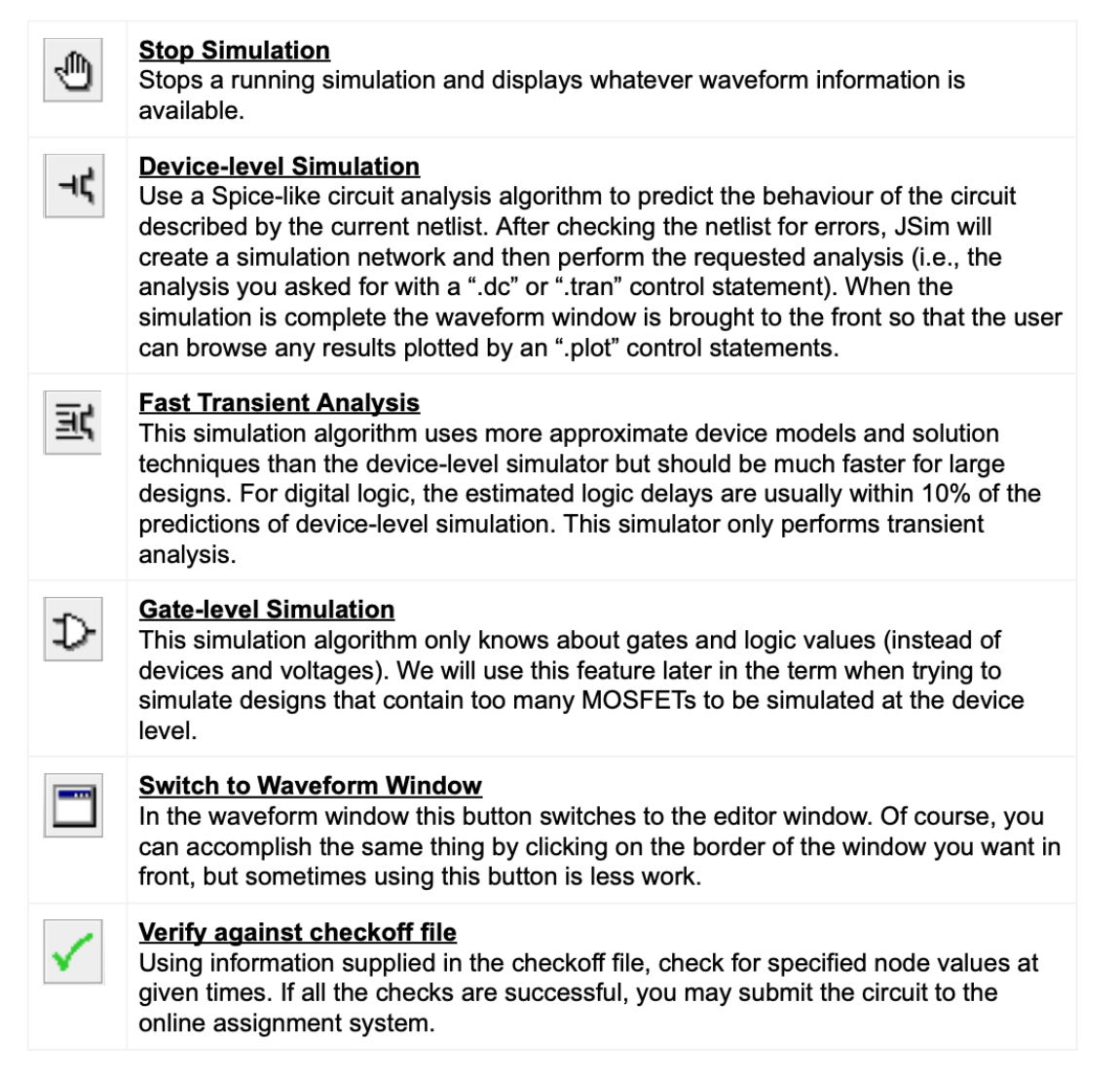
Each icon has the following meaning:
JSim netlist format
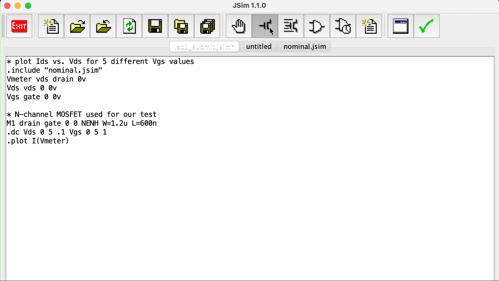
This sample code is a setup to characterise an NFET with the following setup:
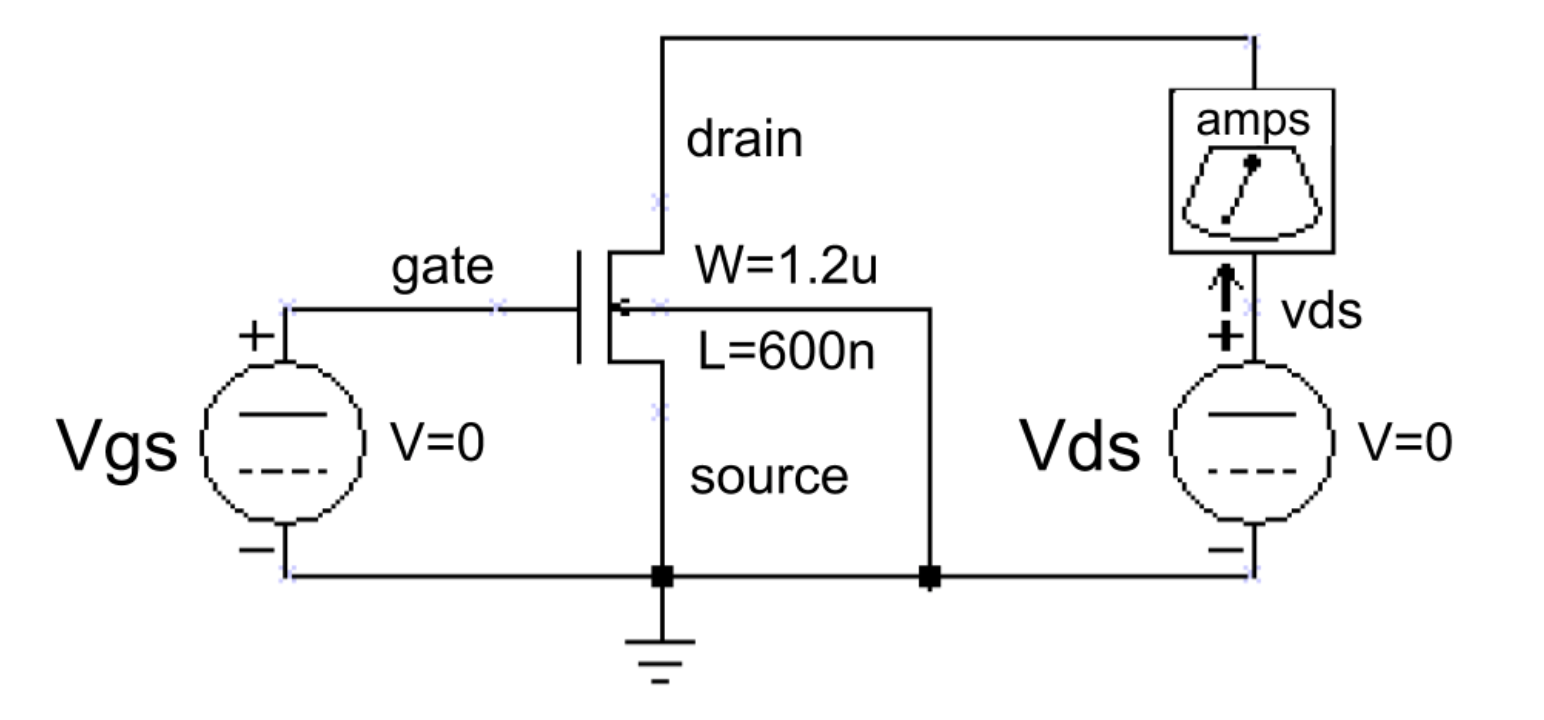
* plot Ids vs. Vds for 5 different Vgs values //1
.include "nominal.jsim" //2
Vmeter vds drain 0v     //3
Vds vds 0 0v            //4
Vgs gate 0 0v           //5

* N-channel MOSFET used for our test  //6
M1 drain gate 0 0 NENH W=1.2u L=600n  //7
.dc Vds 0 5 .1 Vgs 0 5 1              //8
.plot I(Vmeter)                       //9
The JSim netlist format is quite similar to that used by SPICE, a well-known circuit simulator. Each line of the netlist is one of the following:
- Comment line
- Indicated by an
*(asterisk) as the first character. - Comment and blank lines are ignored when JSim processes your netlist
- C++/Java style comments can also be used
//, all characters starting with this and to the end of the line are ignored./*and*/, any lines or parts of lines enclosed by these are ignored.
- Indicated by an
- Continuation line
- Indicated by a
+as the first character. - Treated as if they had been typed at the end of the previous line (without the
+of course) - No limit to length of an input line, but breaking long lines using
+makes it easier to edit and understand +also continues comment lines
- Indicated by a
- Control statement
- Indicated by
.(period) as the first character. - Provides information about how the circuit is to be simulated
- Indicated by
- Circuit element
- Indicated by a letter as the first character, that represents the type of circuit element. e.g.
rfor resistor,cfor capacitor,mfor MOSFET,vfor voltage source. - Remainder of line specifies which circuit nodes connect to which device terminals and any parameters needed by that type of circuit element. For example, the following line describes a 1000Ω resistor called
R1that connects to nodesAandB:R1 A B 1k
- Indicated by a letter as the first character, that represents the type of circuit element. e.g.
Note
The numbers can be entered using engineering suffixes for readability. Common suffixes are:
- kilo: “k” = 1000
- micro: “u” = 1E-6
- nano: “n” = 1E-9
- pico: “p” = 1E-12
With that knowledge in mind, the code snippet above has the following meaning:
| Line | Description |
|---|---|
| 1, 6 | A comment. Any line that begins with a * signifies a comment. |
| 2 | A control statement that directs JSim to include a netlist file containing the MOSFET model parameters for the manufacturing process we will be targeting this semester. The pathname shown MUST be MODIFIED to point at where your nominal.jsim file is located |
| 3-5 | These specify three voltage sources; each voltage source specifies the two terminal nodes and the voltage we want between them. Note that the reference node for the circuit (marked with a GROUND symbol in the schematic) is always called 0. The v following the voltage specification is not a legal scale factor and will be ignored by JSim–it is included just to remind ourselves that the last number is the voltage of the voltage source. All three sources are initially set to 0 volts but the voltage for the Vds and Vgs sources will be changed later when JSim processes the .dc control statement. We can ask JSim to plot the current through voltage sources which is how we’ll see what Ids is for different values of Vgs and Vds. We could just ask for the current of the Vds voltage source, but the sign would be wrong since JSim uses the convention that positive current flows from the positive to negative terminal of a voltage source. So we introduce a 0V source with its terminals oriented to produce the current sign we’re looking for. |
| 7 | This is the MOSFET. We have described in the following order: drain, gate, source and substrate nodes (in this order!). For instance, MPD1 z a 1 0 NENH sw=8 sl=1 signifies that drain is connected to node z, gate to node a, source to node 1 (this is NOT VDD) bulk to node 0 (ground). The next item names the set of model parameters JSim should use when simulating this device; “NENH” for an NFET, and “PENH” for a p-channel MOFET (PFET). The final two entries specify the width and length of the MOSFET. Note that the dimensions are in microns (1E-6 meters) since we’ve specified the u scale factor as a suffix. Do not forget the u or your MOSFETS will be meters long! You can always use scientific notation (e.g., 1.2E-6) if suffixes are confusing. |
| 8 | A control statement requesting a DC analysis of the circuit made with different settings for the Vds and Vgs voltage sources: the voltage of Vds is swept from 0V to 5V in .1V steps, and the voltage of Vgs is swept from 0V to 5V in 1V steps. Altogether \(51 \times 6\) separate measurements will be made. |
| 9 | A control statement that gets JSim to plot the current through the voltage source named Vmeter. JSim knows how to plot the results from the dual voltage sweep requested on the previous line: it will plot I(Vmeter) versus the voltage of source Vds for each value of voltage of the source Vgs. There will be 6 plots in overall, each consisting of 51 connected data points. |
Waveform Window
After you enter the netlist above, you might want to save your efforts for later use by using the save file button. To run the simulation, click the device-level simulation”button on the toolbar. After a pause, a waveform window will pop up and we can take some measurements.
Controls:
- As you hover the mouse over the waveform window, a moving cursor will be displayed on the first waveform above the mouse’s position and a readout giving the cursor coordinates will appear in the upper left hand corner of the window.
- To measure the delta (difference) between two points, position the mouse so the cursor is on top of the first point.
- Now click left and drag the mouse (i.e., move the mouse while holding its left button down) to bring up a second cursor that you can then position over the second point.
- The readout in the upper left corner will show the coordinates for both cursors and the delta between the two coordinates.
- You can return to one cursor by releasing the left button.
In the example above, we only have one channel. The waveform window shows various waveforms in one or more channels (rows) in general. Initially one channel is displayed for each .plot control statement in your netlist. If more than one waveform is assigned to a channel, the plots are overlaid on top of each using a different drawing color for each waveform. If you want to add a waveform to a channel simply add the appropriate signal name to the list appearing to the left of the waveform display (the name of each signal should be on a separate line).
You can also add the name of the signal you would like displayed to the appropriate .plot statement in your netlist and rerun the simulation. If you simply name a node in your circuit, its voltage is plotted. You can also ask for the current through a voltage source by entering I(Vid).
The waveform window has several other buttons on its toolbar:
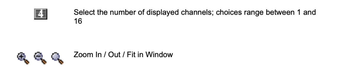
Zoom, Pan, Center
You can zoom and pan over the traces in the waveform window using the controls found along the bottom edge of the waveform display. The scrollbar at the bottom of the waveform window can be used to scroll through the waveforms. To recentre the waveform about a particular point, place the cursor at that position and press c.
Defining Circuit Elements Using .subckt
You can create your own custom circuit elements made of various MOSFETs using .subckt keyword. The following JSim netlist shows you how to define your own circuit elements using the .subckt statement:
.include "nominal.jsim"

* 2-input NAND: inputs are A and B, output is Z
.subckt nand2 a b z
MPD1 z a 1 0 NENH sw=8 sl=1
MPD2 1 b 0 0 NENH sw=8 sl=1
MPU1 z a vdd vdd PENH sw=8 sl=1
MPU2 z b vdd vdd PENH sw=8 sl=1
.ends

* INVERTER: input is A, output is Z
.subckt inv a z
MPD1 z a 0 0 NENH sw=16 sl=1
MPU1 z a vdd vdd PENH sw=16 sl=1
.ends
The .subckt statement introduces a new level of netlist.
- All lines following the
.subcktup to the matching.endsstatement will be treated as a self-contained subcircuit. - This includes model definitions, nested subcircuit definitions, electrical nodes and circuit elements.
- Remember the order of mosfet node declaration: drain gate source substrate(bulk)
MPD1 z a 1 0 NENH sw=8 sl=1signifies that drain is connected to nodez, gate to nodea, source to node1(this is NOT VDD) bulk to node0(ground)- Notice how the source node of MPD1 is connected to the drain node of MPD2, which means that both NFETs are connected in series
- Both PFETs are connected in parallel (by CMOS rule)
The only parts of the subcircuit visible to the outside world are its terminal nodes which are listed following the name of the subcircuit in the .subckt statement:
.subckt name terminals…
* internal circuit elements are listed here
.ends
In the example netlist, two subcircuits are defined:
nand2which has 3 terminals nameda,bandzinside thenand2subcircuitinvwhich has 2 terminals namedaandz
Using Subcircuits
Once the definitions are complete, you can create an instance of a subcircuit using the X circuit element:
Xid nodes… name
where:
name: the name of the circuit definition to be used,id: a UNIQUE name for this instance of the subcircuitnodes…: the names of electrical nodes that will be hooked up to the terminals of the subcircuit instance
There should be the same number of nodes listed in the X statement as there were terminals in the .subckt statement that defined name.
For example, here’s a short netlist that instantiates 3 NAND gates (called g0, g1 and g2):
Xg0 d0 ctl z0 nand2
Xg1 d1 ctl z1 nand2
Xg2 d2 ctl z2 nand2
Explanation:
- The node
ctlconnects to all threenand2gates instances; all the other terminals are connected to different nodes. - Note that any nodes that are private to the subcircuit definition (i.e. nodes used in the subcircuit that don’t appear on the terminal list) will be unique for each instantiation of the subcircuit (like local variables):
- For example, there is a private node named
1used inside thenand2definition. - When JSim processes the three
Xstatements above, it will make three independent nodes calledxg0.1,xg1.1andxg2.1, one for each of the three instances ofnand2. - There is no sharing of internal elements or nodes between multiple instances of the same subcircuit.
- The example netlist above uses
vdd(jsim standard for power source) whenever a connection to the power supply is required.
- For example, there is a private node named
Shared Nodes
There are two common shared nodes in jsim: vdd and 0. Please do not use these to name your custom electrical nodes.
It is sometimes convenient to define nodes that are shared by the entire circuit, including subcircuits; for example, power supply nodes. The ground node 0 is such a node; all references to 0 anywhere in the netlist refer to the same electrical node. The included netlist file nominal.jsim defines another shared node called vdd using the following statements:
.global vdd
VDD vdd 0 3.3v
The example netlist above allows us to use vdd whenever a connection to the power supply is required.
Symbolic Dimensions
The other new twist introduced in the example netlist is the use of symbolic dimensions for the MOSFETs (SW= and SL=) instead of physical dimensions (W= and L=). Symbolic dimensions specify multiples of a parameter called SCALE, which is also defined in nominal.jsim:
.option SCALE=0.6u
So with this scale factor, specifying SW=8 is equivalent to specifying W=4.8u.
Using symbolic dimensions is encouraged since it makes it easier to determine the W/L ratio for a MOSFET (the current through a MOSFET is proportional to W/L) and it makes it easy to move the design to a new manufacturing process that uses different dimensions for its MOSFETs. Note that in almost all instances SL=1 since increasing the channel length of a MOSFET reduces its current carrying capacity, not something we’re usually looking to do.
We’ll need to keep the PN junctions in the source and drain diffusions reverse biased to ensure that the MOSFETs stay electrically isolated, so the substrate terminal of NFET (those specifying the NENH model) should always be hooked to ground (node 0). Similarly the substrate terminal of PFET (those specifying the “PENH” model) should always be hooked to the power supply (node vdd).
Perform .dc analysis
we’ll perform a dc analysis to plot the gate’s output voltage as a function of the input voltage using the following additional netlist statements. Paste this under the nand2 and inverter declaration you made above in the new file.
* dc analysis to create VTC
Xtest vin vin vout nand2
Vin vin 0 0v

Vol vol 0 0.3v
Voh voh 0 3v

.dc Vin 0 3.3 .005
.plot vin vout voh vol
Click the device-level simulation button to view the output waveform window.
How MOSFET width and length affects VTC
The length (L) and width (W) of a MOSFET (Metal-Oxide-Semiconductor Field-Effect Transistor) have significant effects on the Voltage Transfer Characteristics (VTC) of logic gates made from these transistors. Here’s a detailed look at how these dimensions affect the MOSFET’s performance and, consequently, the VTC of the gates:
1. Effect on Drive Current
-
Width (W): Increasing the width of the MOSFET increases the channel area, allowing more electrons (or holes in a pMOS) to flow from the source to the drain. This increases the drive current (called \(I_{DS}\), or I Drain-Source) of the MOSFET. A higher drive current can result in faster switching speeds and lower resistance in the on-state, which influences the VTC by making the transitions sharper.
-
Length (L): Decreasing the length of the MOSFET reduces the distance electrons have to travel, which also increases the drive current. A shorter channel length leads to higher electron mobility and a higher current for a given gate voltage (called \(V_{GS}\) or V Gate-Source).
2. Threshold Voltage (Vth) and Subthreshold Characteristics
-
Short Channel Effects: Reducing the length can lead to short-channel effects (please do further search if you’ve never heard of this term), such as threshold voltage roll-off and drain-induced barrier lowering, which can impact the VTC. These effects can cause the MOSFET to turn on at lower gate voltages, affecting the VTC’s shape and the voltage levels at which the transitions occur.
-
Width Effects: While width primarily affects the current capability, very narrow devices can suffer from increased variability and edge effects that might slightly alter VTC characteristics.
3. Capacitance and Switching Speed
- Width and Capacitance: A wider MOSFET has a larger gate capacitance (\(C_G\)).
- Higher capacitance requires more charge to change the voltage, which can slow down the switching speed if the driving current is not increased proportionally.
- While the VTC plot itself does not directly indicate switching speed, the increased capacitance can indirectly affect the dynamic response of the gate.
4. Impact on VTC
-
Drive Strength: Both increased width and decreased length result in higher drive strength, which sharpens the transition region of the VTC. A sharper transition region implies that the output voltage (Vout) changes more sensitively and distinctly for a given change in input voltage (Vin).
-
Sensitivity: The VTC shows the sensitivity of Vout to changes in Vin. Higher drive strength due to optimal width and length dimensions can make the inverter more sensitive, meaning it has a steeper slope in the transition region.
5. Practical Considerations
- Trade-offs: Increasing the width or decreasing the length improves current drive but also increases power consumption and chip area. There is always a trade-off between speed, power, and area in MOSFET design.
Conclusion
The physical dimensions of a MOSFET, particularly its length and width, significantly influence its electrical characteristics, including the current drive capability and threshold voltage. These changes affect the Voltage Transfer Characteristics (VTC) of logic gates made from these MOSFETs by altering the steepness and position of the transition region. While the VTC plot itself does not show how fast the signal changes (which is more related to dynamic performance and capacitance), it shows how sensitively the output voltage responds to the input voltage, which is indirectly influenced by the MOSFET’s physical dimensions.