 50.002 CS
- 1D Part 1 - Mini Hardware Project
50.002 Computation Structures
Information Systems Technology and Design
Singapore University of Technology and Design
Written by: Natalie Agus (2023)
1D Part 1 - Mini Hardware Project
This project is part 1 of your 1D project (with part 2 being your Electronic Game Hardware Project, details in the course handout). This part 1 weighs 4% of your total assessment, while part 2 weighs 25%. The goal of this project is to familiarise yourself with:
- The behavior of a few logic gates,
- Basic wiring and using the breadboard
- Soldering various hardware components: switches, LEDs, resistors, logic gates
By the end of this project you should be able to:
- Measure static input-output relationship of the logic gates.
- Design a simple 1 bit digital adder.
- Examine the functionality of a simple digital adder.
- Implement a simple digital adder on a strip-board with a user interface.
Deliverables
You have to complete 3 parts to do to score all 4% components of MHP:
- Part A (0.5%): Answer related questions about this handout on eDimension (Task 1-7, Task 9-12)
- Part B (0.5%): Assemble 1-bit HALF adder on a breadboard and checkoff in class with a TA or Instructor (Task 8)
- Part C (3%): Make a 1-bit FULL adder using basic logic gates provided in your 1D kit, and solder the circuit on a stripboard (Week 4 due). See this handout for further submission details and sample submission photo.
Basics of Breadboard
The breadboard can be use to prototype your circuit design fast without the need to solder anything. Take out a breadboard, battery pack, LED, resistor, a few jumper wires, and assemble the following simple circuit.
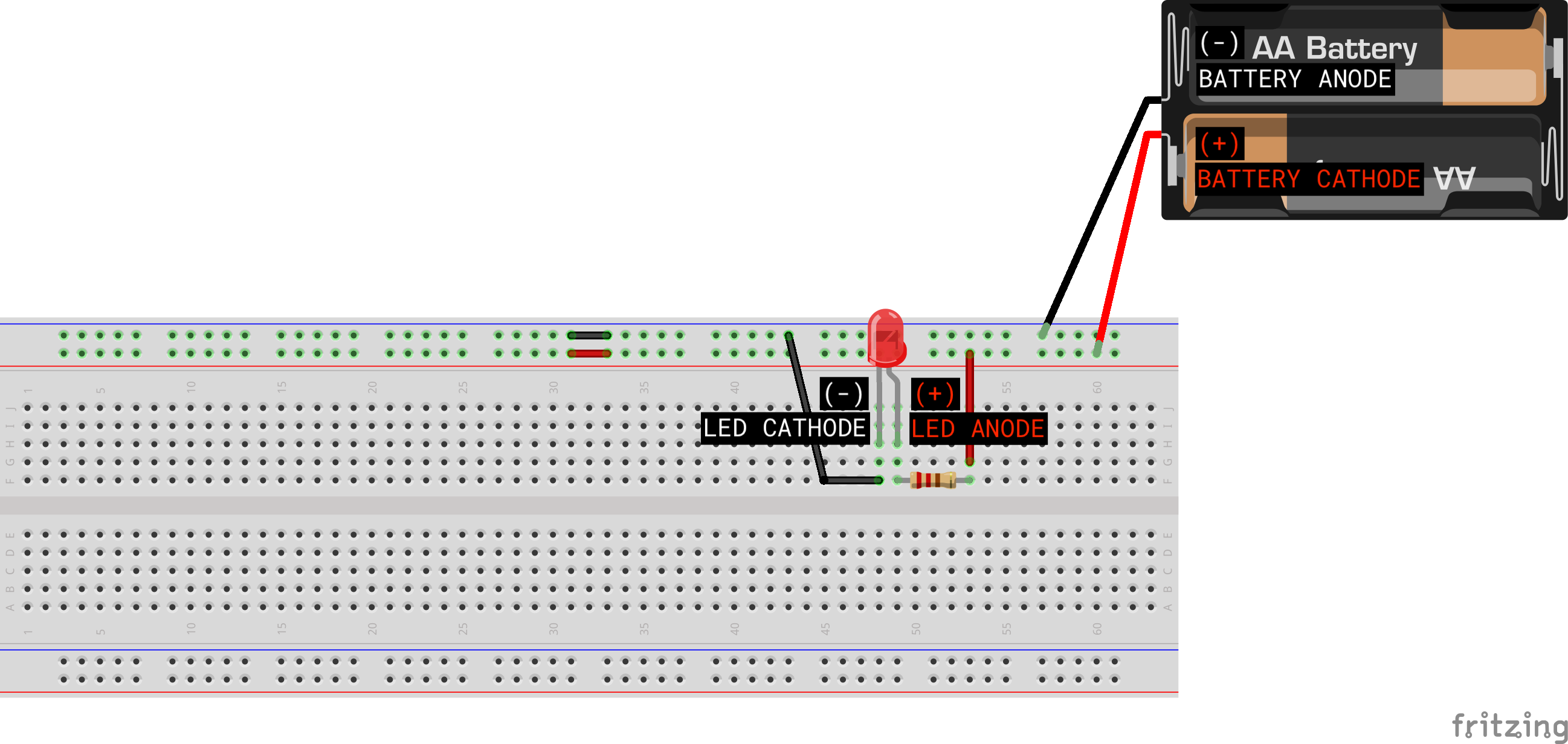
The two horizontal rows at the top and the bottom of the breadboard (when viewing the breadboard this way) are connected horizontally and are usually used for power and ground lines. Each vertical column (labeled 1 to 63 above) are connected vertically.
The battery’s positive terminal (cathode or VDD) and negative terminal (anode or GND) terminals are connected to each of the first two rows in the breadboard. These can be considered as the “power lines”.
The LED is connected at column 48 and 49 as shown above:
- The longer leg (called anode or “positive” side) is connected at column 49
- Yes, this is not a typo
- The shorter leg (called cathode, or “negative” side) is connected at column 48
- Electrons will travel from anode (positive side) to cathode (negative side) and never the other way around
The thing to remember is that conventional current always flows from cathode to anode in the external circuit (not internally through the object of interest!). Since the direction of electrons is opposite of current, the electrons in the external circuit move towards the (+) terminal of the battery cell, which makes it a cathode. By extension, the battery’s (-) terminal is the anode.
For the LED bulb, there exist a diode in it so that current flows through it from the anode (longer leg) to the cathode (shorter leg) and never the opposite direction. Remember that anywhere in the circuit (external to the battery and the LED bulb) current always flows from cathode to anode.
See the diagram below to let it sink in. Ask yourself, which way the current flows? Clockwise or anticlockwise? Then, which way the electron flows?
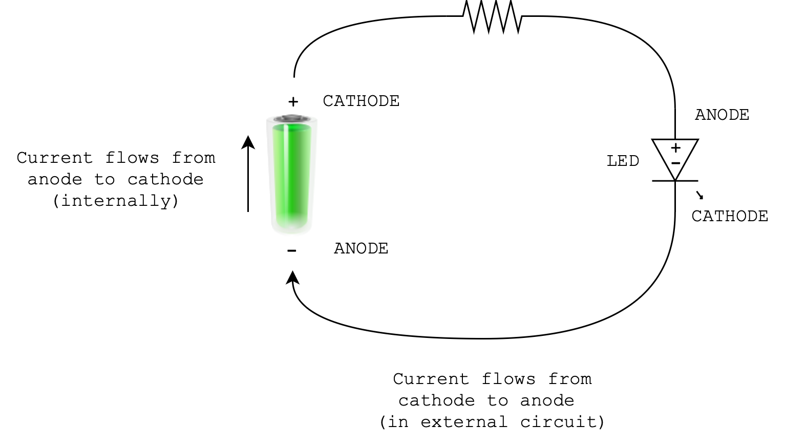
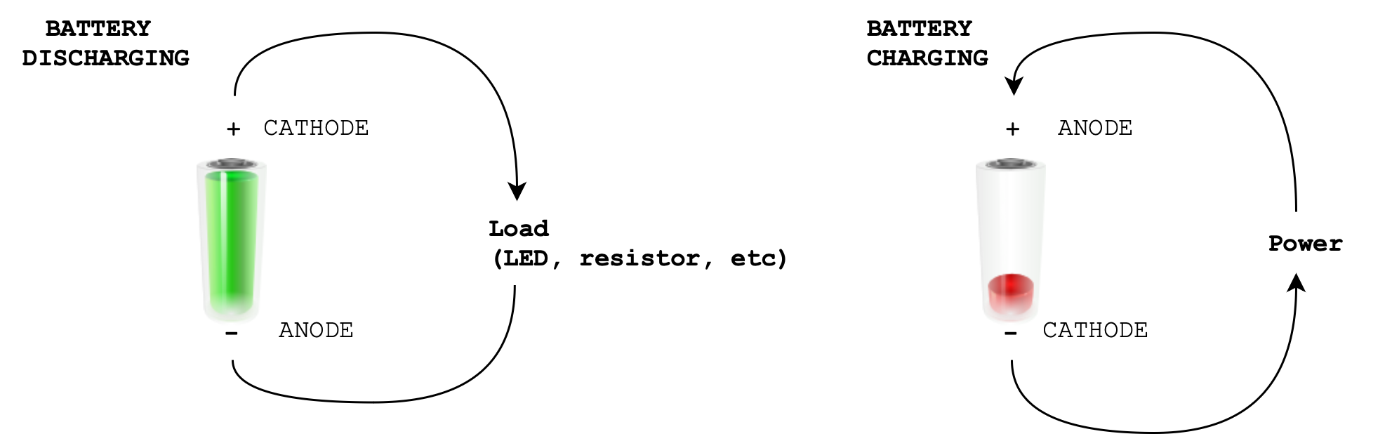
Also, the name “cathode” or “anode” on the battery’s terminal depends on whether the battery is charging or discharging. One fact remains the same: conventional current always flows from cathode to anode. We can rename the terminals based on the direction of current flow.
The LED is connected in series with the resistor (it’s beyond this class to compute how many Ohm is needed, but you can easily google it). A resistor is needed to not blow up the LED. An AA battery supplies 1.5V each. If you use a 4-battery pack, it will supply 6V, if you use a 2-battery pack, it will supply 3V. A typical LED requires only approximately 2V and 20mA (depends on the color and size).
Take a look at basic documentation of a 5mm red LED vs 5mm blue LED vs 10 mm super bright red LED. They are all different.
That means given a 4-battery pack power supply ($V_{dd}$ = 6V) and a single 2V, 20mA small LED, we need a resistor with value of:
\[R = \frac{V_{dd}-V_{led}}{I_{led}} = \frac{6-2}{0.02} = 200 \Omega\]Task 1
Light up the LED
Ensure that you can assemble the circuit above and get your LED lit up before proceeding.
Why does the LEDs light up?
Let’s do some quick recap. The battery’s (+) terminal is connected to the LED’s longer leg (after passing the resistor) and the battery’s (-) terminal is connected to the LED’s shorter leg, thereby closing the circuit. The LED lights up because there exists a potential difference between the battery’s (+) terminal and the battery’s (-) terminal, and there exist current flowing within the closed circuit which dissipates power (to light up the LED).
Head to eDimension and answer a few questions pertaining to this task.
Logic Gates
We have provided a few logic gates in the box as shown. Click on the corresponding datasheet to know what each pin is for.
| Component | Description | Datasheet |
|---|---|---|
| 74HC00 | Quad 2-input NAND gate | 74HC00.pdf |
| 74HC02 | Quad 2-input NOR gate | 74HC02.pdf |
| 74HC04 / 74H04 | Hex inverting buffer gate | 74HC04.pdf |
| 74HC08 | Quad 2-input AND gate | 74HC08.pdf |
| 74HC32 | Quad 2-input OR gate | 74HC32.pdf |
| 74HC86 | Quad 2-input exclusive OR gate | 74HC86.pdf |
Let’s figure out the functionality of each of these logic gate by assembling them on the breadboard.
- How exactly these gates work and what electronic components make up these logic gates is a complex issue
- We will give an overview at the end of this handout, and in the following lectures. Please bear with us for now
- Let’s begin by examining its functionality first before later studying how it works
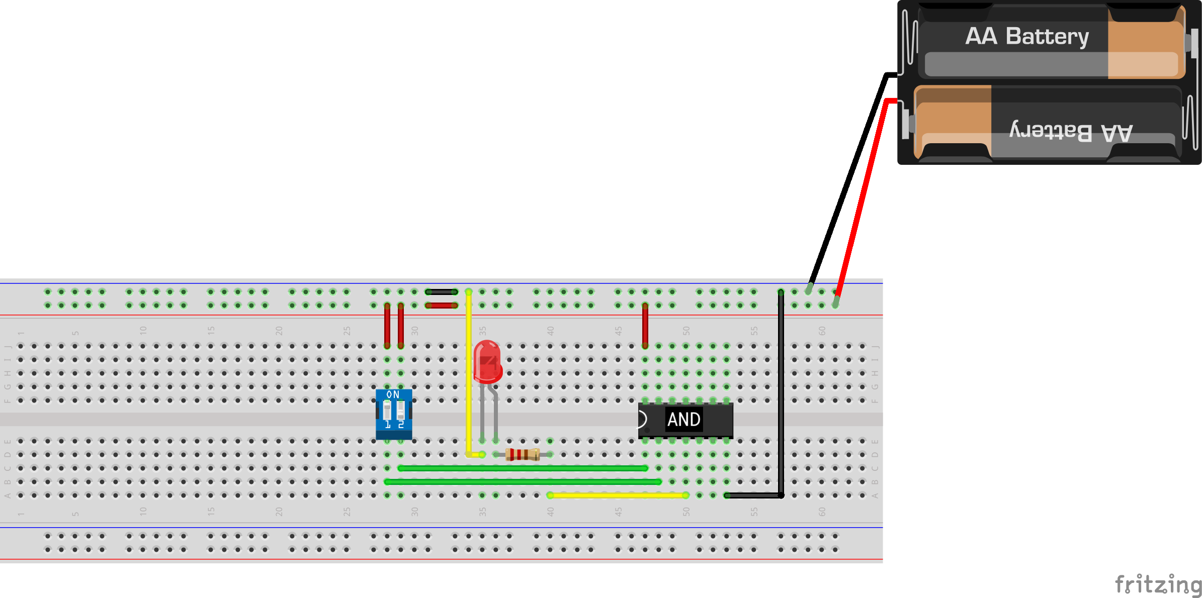
74HC00
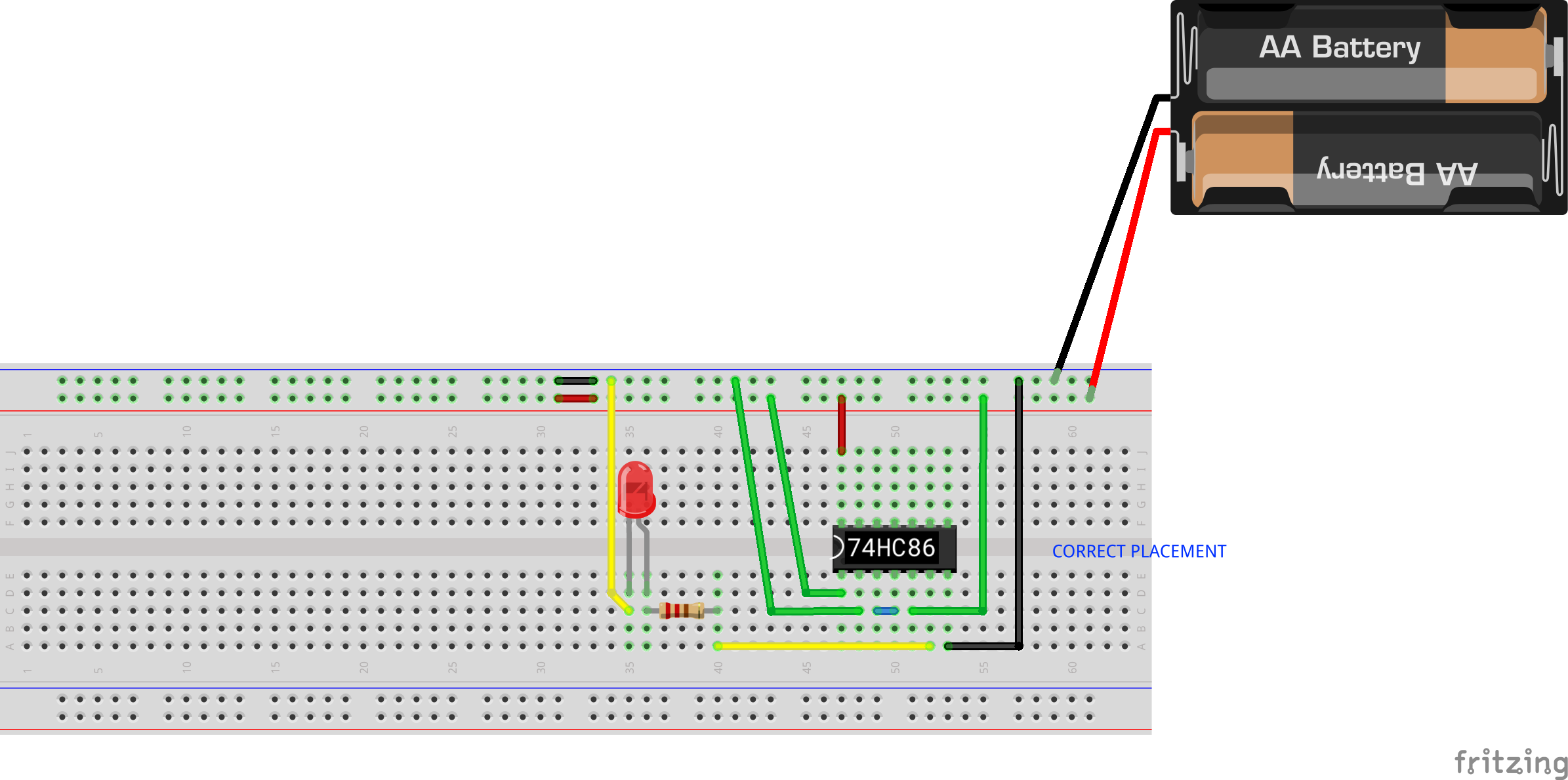
Let’s take into example this Quad NAND gate (74HC00). Assemble it on your breadboard as follows. Please note the orientation of the notch, and also please ensure that the gate is placed correctly on the breadboard:
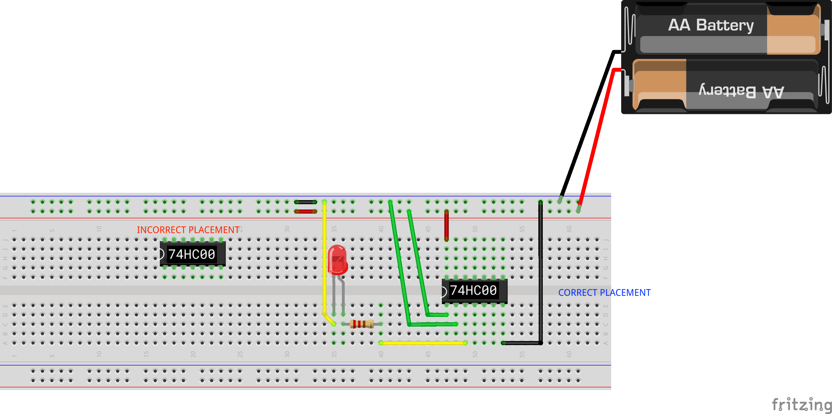
If you open its datasheet, you’ll notice that it has 14 pins labeled as 1 to 14. The figure on the right shows the functionality of each of this pin. It shows that there are four independent NAND gates inside 74HC00 (it’s like buy 1 get 3 free).
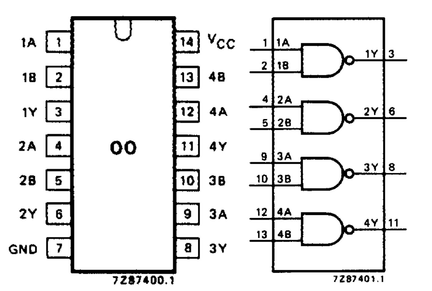
To power on the logic gate, pin 7 is to be connected to GND (negative terminal of your battery) and pin 14 is to be connected to VCC (also known as VDD, which is the positive terminal of your battery). Then we can supply inputs at pin 1 (1A) and pin 2 (1B), and read the output at pin 3 (1Y).
- If we supply inputs at pin 12 (4A) and 13 (4B), we can read the output at pin 11 (4Y)
- The same logic goes to the rest of the pins
Remember that (1A, 1B, 1Y), (2A, 2B, 2Y), (3A, 3B, 3Y), (4A, 4B, 4Y) are all independent of each other. They are 4 separate logic gates. It’s just that they’re all soldered together into a little chip for economic reason (it’s more expensive to buy 4 separate ones).
Supply Input
The inputs in the above breadboard schematic is represented by the green wires (there are two input lines), connected to pin 1 (1A) and 2 (1B) of the 74HC00 respectively.
We connect one of the green wires to positive terminal of the battery, and the other green wire to the negative terminal of the batteries. This represents a digital input of 1 at pin 1 (1A) and a digital input of 0 at pin 2 (2A),
Read Output
The output is represented by the yellow wire in the breadboard schematic. We use an LED to read the output signal. If the LED is on, then the output corresponds to digital value 1 (basically high voltage), and if the LED is off, then the output corresponds to digital value 0 (basically low voltage).
Terminologies
Digital value 1
For the purpose of this lab, when the LED is ON, it means that pin 3 (1Y) supplies a high voltage (which results in current flowing through the LED and power dissipated to light up the bulb). Let’s name this HIGH VOLTAGE condition as digital value 1. In other words, we say that pin 3 (1Y) supplies digital value 1 to the LED if the LED is lit up.
The LED itself is just a “tool” that we use to read the voltage value of pin 3 (1Y). If the voltage is HIGH enough, our LED is ON. Otherwise, our LED is OFF. We don’t really care about the actual voltage value of pin 3 (1Y), only that it is a HIGH VOLTAGE: higher than the lowest voltage in the circuit, which is the battery’s (-) terminal.
Digital value 0
Similarly, for the purpose of this lab, when the LED is OFF (at least to the naked eye), it means that pin 3 (1Y) supplies a low voltage. It does not necessarily mean that it is 0V, but low enough in comparison to the highest voltage point in the entire circuit which is the battery’s (+) terminal. In other words, we say that pin 3 (1Y) supplies digital value 0 to the LED if the led is not lit up.
Again, we don’t really care about the actual low voltage of pin 3 (1Y).
The notion of a “LOW ENOUGH” and “HIGH ENOUGH” voltage which corresponds to digital value 0 and 1 respectively (without caring about its actual numerical value) is called digital abstraction. You will learn it in future lectures.
VDD and GND
If you haven’t realised already, the terms HIGH and LOW voltages are relative and not absolute. The same logic applies to VDD and GND.
The notion of VDD and GND (sometimes illustrated as Vss) terminal does not imply anything about its actual numerical voltage value. VDD simply means the positive supply voltage which is the highest voltage point value in your entire circuit. Simply, GND (stands for ground) simply means the lowest voltage value in your entire circuit and it does not always mean 0V. Current flows from VDD to GND in the circuit because it always flows from high voltage point to low voltage point.
That’s why it is important for your circuit to have a common ground so that they can agree on what is the value of the lowest voltage point in the entire circuit.
Please consult your freshmore faculties who taught you circuits and electronics if you have forgotten about this.
Task 2
The logic of 74HC00
Assemble the circuit as shown in the breadboard schematic above and observe if the LED is ON or OFF with that exact arrangement. Then, try supplying both
0at pin 1 and pin 2 by plugging both green wires at the battery’s GND line (-). Is the LED ON or OFF?
Complete the truth table below by varying the inputs at pin 1 and pin 2 of 74HC00. Key in your answer on eDimension.
| 74HC00 Pin 1 (1A) | 74HC00 Pin 2 (1B) | LED (ON/OFF) Pin 3 (1Y) 74HC00 |
|---|---|---|
| 0 | 0 | ? |
| 0 | 1 | ? |
| 1 | 0 | ? |
| 1 | 1 | ? |
Let’s do a little Quiz to test your understanding.
Task 3
The logic of 74HC02, 74HC08, 74HC32, and 74HC86
Replace 74HC00 with one of these logic gates and repeat the procedure of observing the LED output by varying inputs to pin 1 and pin 2.
Complete the truth table below by varying the inputs at pin 1 and pin 2 of each logic gate. Key in your answer on eDimension.
| Pin 1 (1A) | Pin 2 (1B) | LED (ON/OFF) Pin 3 (1Y) 74HC02 | LED (ON/OFF) Pin 3 (1Y) 74HC08 | LED (ON/OFF) Pin 3 (1Y) 74HC32 | LED (ON/OFF) Pin 3 (1Y) 74HC86 |
|---|---|---|---|---|---|
| 0 | 0 | ? | ? | ? | ? |
| 0 | 1 | ? | ? | ? | ? |
| 1 | 0 | ? | ? | ? | ? |
| 1 | 1 | ? | ? | ? | ? |
Task 4
The logic of Inverter 74HC04
Study the datasheet of 74HC04. By now, you should be able to assemble it on your breadboard, supply an input using the wires and read the output using an LED.
Head to eDimension to answer some questions about Task 3 and 4. You might want to do the quiz below first.
More than 2-inputs
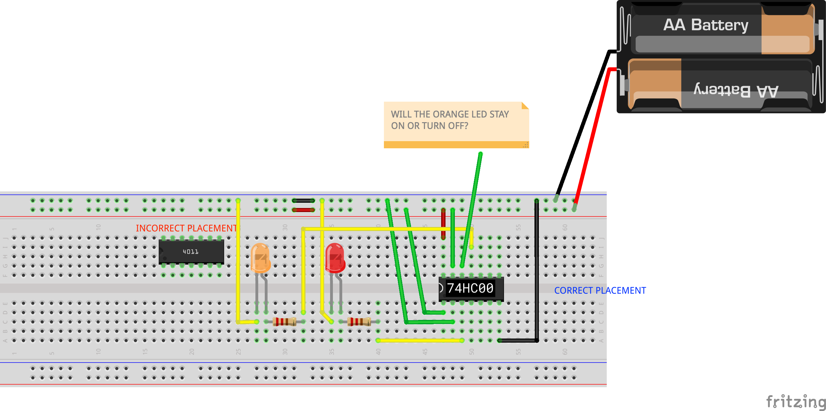
We can create a 3-input NAND/NOR/XOR gates by utilising two gates within each chip. For instance, we can create a 3-input XOR gate using 74HC86 by assembling our components as follows:
Notice that the output of the first XOR gate at pin 3 (1Y) is set as the input of the second XOR gate at pin 4 (2A). A third independent input (green wire) is supplied at pin 5 (2B). Finally, the output is read at the LED via pin 6 (2Y).
Complete the 3-input XOR truth table below by varying the inputs at pin 1, pin 2, and pin 5 of 74HC86. Key in your answer on eDimension.
| 74HC86 Pin 1 (1A) | 74HC86 Pin 2 (1B) | 74HC86 Pin 5 (2B) | LED (ON/OFF) Pin 6 (2Y) 74HC00 |
|---|---|---|---|
| 0 | 0 | 0 | ? |
| 0 | 1 | 0 | ? |
| 1 | 0 | 0 | ? |
| 1 | 1 | 0 | ? |
| 0 | 0 | 1 | ? |
| 0 | 1 | 1 | ? |
| 1 | 0 | 1 | ? |
| 1 | 1 | 1 | ? |
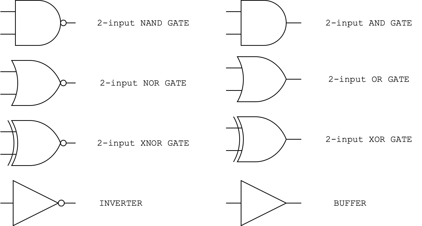
Symbols
Each logic gate above has a symbol that is often used to easily illustrate their arrangement in a circuit. Please remember the symbols for each of these basic logic gates. You will need it to survive this subject.
1-bit Half Adder
We can use these basic logic gates: NOR, NAND, XOR, and INV to form a more complex logic such as addition. We can perform addition easily in base 10 (decimal). Suppose we have single digit addition, then our output may overflow:
- 5+5 = 10 (with carry out or overflow, where the output digit is more than each of the input digit)
- 9+5 = 14 (also has carry out or overflow)
- 1+1 = 2 (no overflow, carry out value is 0)
- 2+5 = 7 (no overflow, carry out value is 0)
Why care about overflow?
You don’t usually care about overflow when you’re just using your computers to compute these measly numbers. But, imagine you’re making or buying a hardware (like neon sign) to hold each of these numbers to display in front of a shop. You will first consider how many digits at maximum each number can hold so you can buy the correct neon sign.
Now, we need to perform addition using base 2 (instead of base 10). In base 2, you have only two values per digit: 0 and 1 while in base 10 you have 10 different values: 0 to 9.
A single digit in base 2 is called a bit. No, no pun intended.
Task 5
Half adder logic
Perform a literature search about logic gate adder, which is the most fundamental logic in your CPU. Then fill up the truth table below that represents the logic of a 1-bit adder. In Lab 2, we will learn how to assemble the circuitry of n-bit adder.
Head to eDimension to answer questions pertaining to this task.
| A (Input 1) | B (Input 2) | Co (Carry out) | S (Sum) |
|---|---|---|---|
| 0 | 0 | ? | ? |
| 0 | 1 | ? | ? |
| 1 | 0 | ? | ? |
| 1 | 1 | ? | ? |
Task 6
Assemble Carry Out
Draw the schematic of the gate level half-adder using the gate symbols shown to you in the previous section. This helps you visualise the schematic of the half adder unit. Then, assemble the carry out unit on a breadboard.
Follow the schematic below. Make sure you use the right logic gate to compute the Carry Out bit:
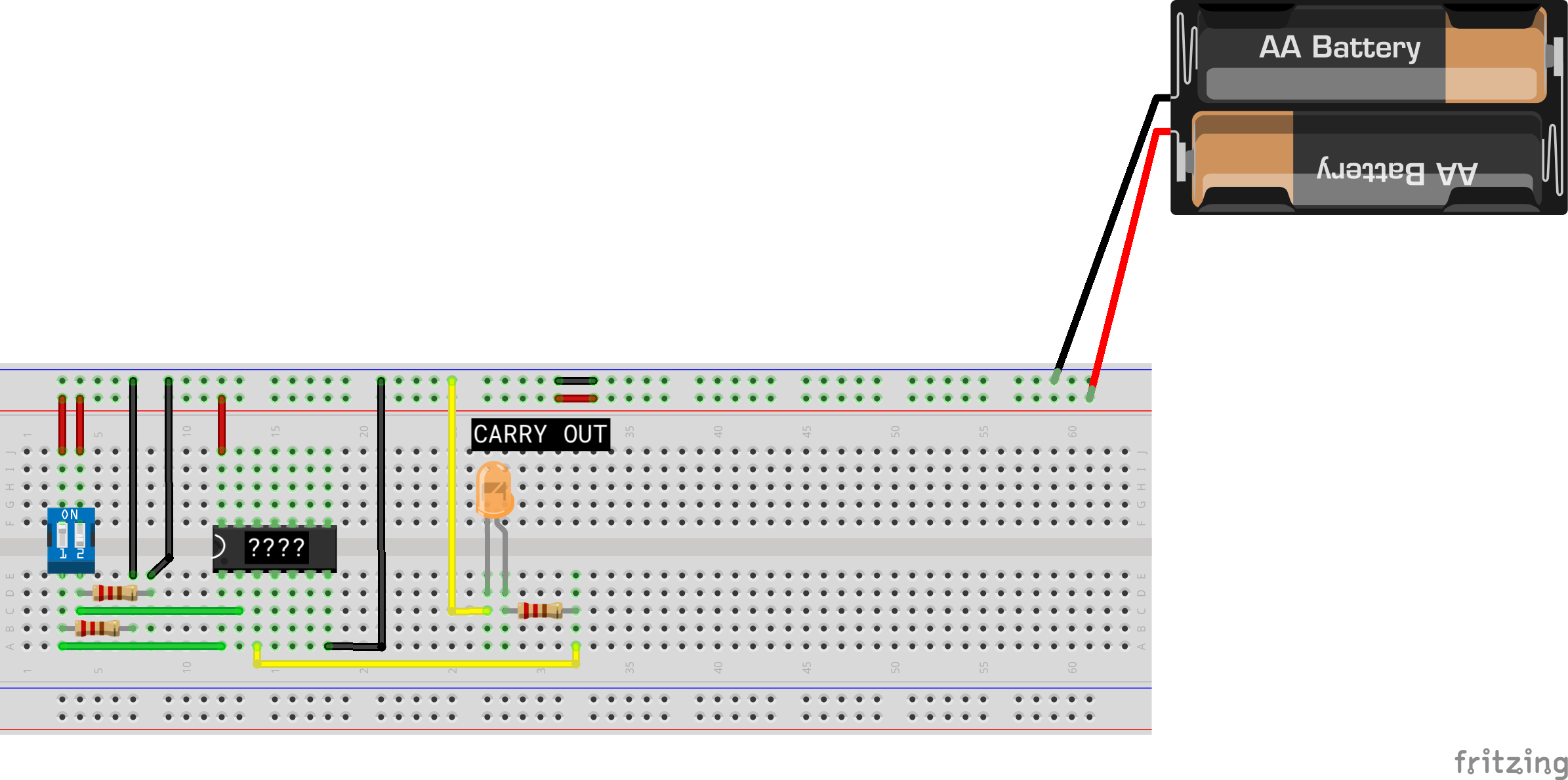
Notice the presence of two resistors below the switch. These are called the pulldown resistors. We will explain its purpose later. For now, just follow the diagram closely.
Do not forget to test your carry out by using the dipswitch and observing if the LED is lit up only when both of the switches are ON.
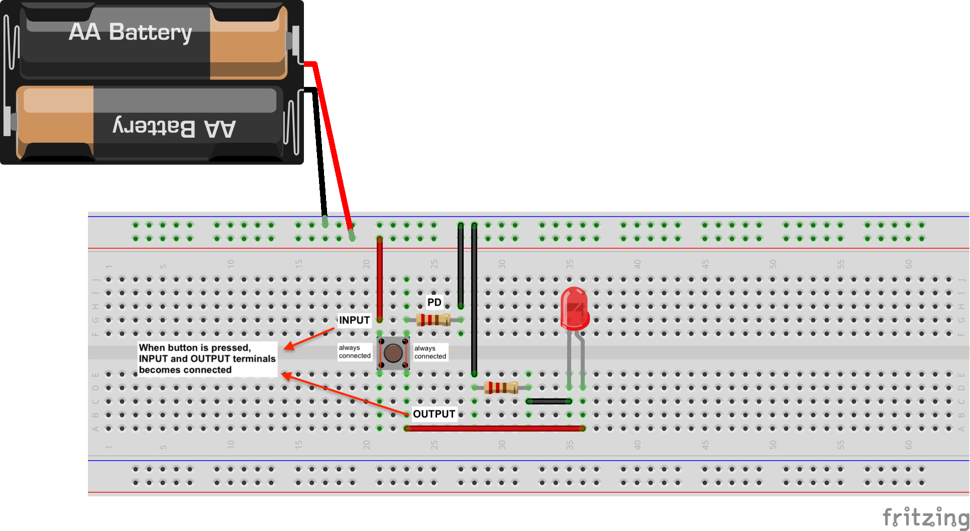
Using Push Button
If you’re given push buttons instead of switches in your 1D kit, please note the push button’s schematic. Each pin is always connected to the pin across it. When the button is pushed, the connection between a pin and its neighbouring pin is formed:
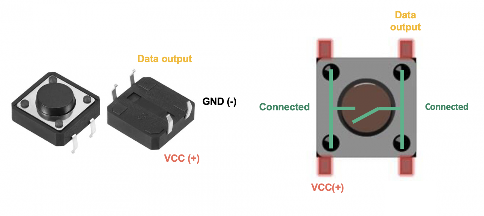
However when the button is released, the circuit is broken and the wire to the LED (or logic gate later on) is known as floating (the voltage is indeterminate) so we need to connect it to ground to ensure the LED/gate receives 0V (OFF):
Each of the pair
Task 7
Assemble Sum
Now, assemble the sum unit on a breadboard.
Follow the schematic below. Make sure you use the right logic gate to compute the Sum bit:
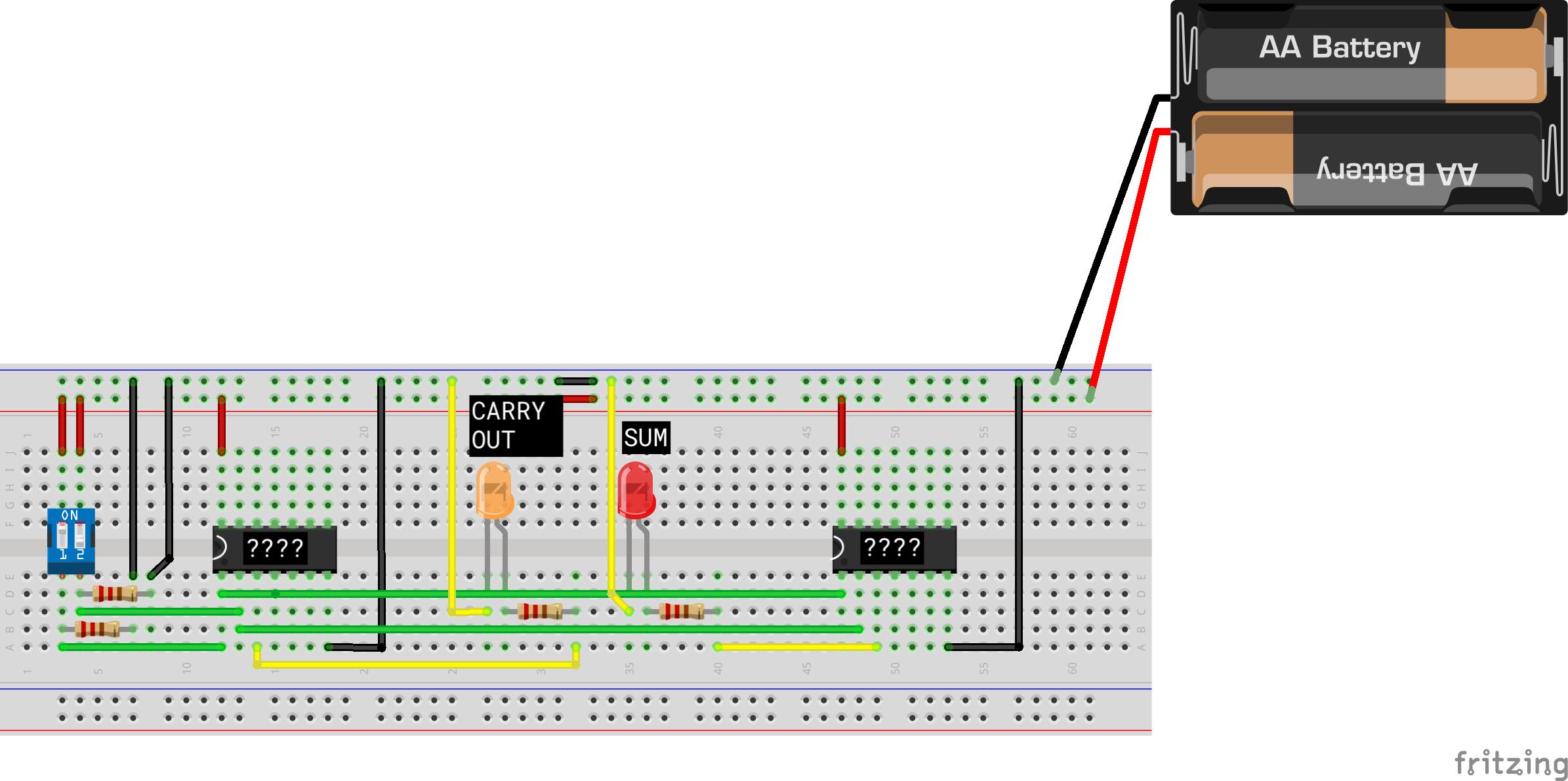
Here’s the equivalent circuit diagram to help you:

Do not forget to test your sum bit by using the dipswitch and observing if the LED is ON up only when ONE of the switches are ON.
Task 8
Checkoff
Approach your TA in class or instructor to give you a checkoff on your half-adder circuit on the breadboard. They will use the switch to supply various input combination. You will obtain 1 mark if circuit shows the functionality of the half adder, and 0 otherwise. There is no half mark, no extension. This 1 mark corresponds to 0.5% of your grade.
If you have a valid LOA in Week 1 during your lab session, you may ask the TA to checkoff in Week 2 by showing them your LOA. If you miss the lab in Week 1 without any LOA, you will obtain a zero.
1-bit Full Adder
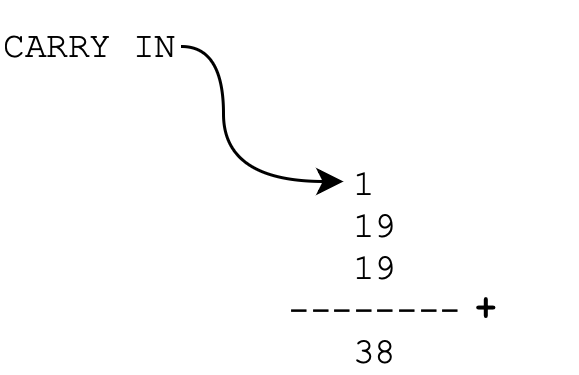
When we do normal additions with two independent inputs in base 10, we actually do not only add two things together but three, because of the carry over from the previous digit. We call this the carry in. See this illustration below:
Right now, our 1-bit half adder does not handle addition of the two existing inputs with the Carry Out (and hence the name: half adder). In a full adder, the addition with the carry out is considered (we cann this carry in).
Task 9
Do some research online and fill up the 1-bit Full Adder truth table below. The last line is already filled up for you. Then head to eDimension to answer questions pertaining to this task.
| A (Input 1) | B (Input 2) | Carry In (Ci) | Carry Out (Co) | Sum (S) |
|---|---|---|---|---|
| 0 | 0 | 0 | ? | ? |
| 0 | 1 | 0 | ? | ? |
| 1 | 0 | 0 | ? | ? |
| 1 | 1 | 0 | ? | ? |
| 0 | 0 | 1 | ? | ? |
| 0 | 1 | 1 | ? | ? |
| 1 | 0 | 1 | ? | ? |
| 1 | 1 | 1 | 1 | 1 |
The last line of the truth table represents the case whereby input 1 is 1, input 2 is 1, and Carry in is 1. This is equivalent to addition 1+1+1, which should result in numerical value 3. The number 3 in base 2 can be represented with binary value 11. The left 1 is Co, and the right 1 is S.
Pulldown Resistor
As promised, we will explain the purpose of adding resistors below the switch. A short explanation is that the pulldown resistor connects unused input pin to ground to keep the given input LOW (equivalent to digital input 0).
Well, won’t disconnecting the switch gives input LOW too? Not necessarily. An “open” wire (disconnected input) has undetermined voltage value.
An Open Wire
Let’s test it by assembling the following circuit on your breadboard. Use the AND gate (74HC08) for this experiment.
Notice that there exist only one resistor for the LED, and no pulldown resistors at the switch.
Task 10
Test whether no input == 0V
Turn ON both switches first so that the LED lits up. Remember, the AND logic dictates that the output is
1when the inputs are BOTH1. Now, GENTLY turn off one of the dipswitch. Ensure you do not touch ANY other part of the circuit while doing this. Just use the tip of a pen to turn off one of the switches. What do you observe? Is the LED still lit up?
You can repeat this experiment 5 more times:
- Flip on both switches, wait until the LED is on
- Gently switch off one dipswitch
- Observe the LED: is it lit up fully? is it half lit? is it fully off?
You will find that the LED will not consistently switch off at step (2).
Why voltage still exists in an open circuit?
If the dipswitch is OFF, then why some voltage is present at the green input wires? You might be confusing current and voltage at this point. Just remember one thing: just because a circuit is open (disconnected), it does not necessarily mean that there exist 0V. Are you shocked? That’s why you can’t just touch any exposed wire in your house. We think this quora answer is simple enough to get you by.
If your LED remains ON even after you off one of the dipswitches, try touching the input wires with your finger ⚡️ to close the circuit and observe what happens. Don’t worry, it’s not harmful.
Now it’s time for some recap and test yourself. Refer to the diagram below to answer the question.
Task 11
Now add a pulldown resistor in the circuit:
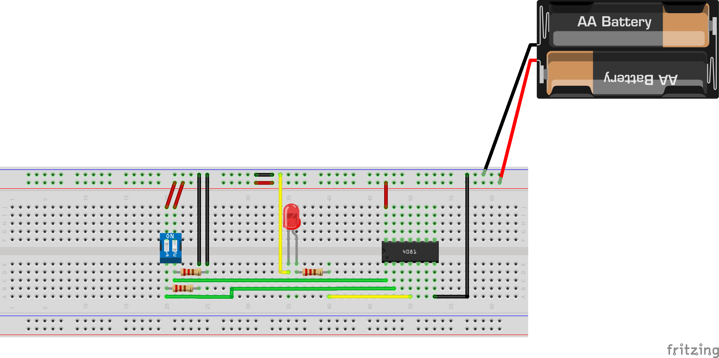
Vary the inputs with the switch and observe that it behaves like a consistent AND logic; that the LED is only lit up when both switches are ON.
The MOSFET
You will learn more on what exactly these gates are in your lecture sessions. These gates are made of MOSFETs (Metal Oxide Seminconductor Field Effect Transistor), and it basically means that they are voltage driven switches. Why do we call these gates a “switch”? Are they the same as dipswitches? Well, kinda.
Refer to this arrangement of the AND gate with the dipswitch:
When we switch ON both of the dip switches, There’s a direct connection between the battery (+) terminal to pin 1 (1A) and pin 2 (1B). We are essentially supplying HIGH VOLTAGE values at pin 1 (1A) and pin 2 (1B). It will then produce HIGH VOLTAGE output at 1Y.
How does the LED bulb light up?
The potential difference between pin 3 (1Y) that’s connected to the longer leg of the LED and the GND or the battery’s (-) terminal that’s connected at the shorter leg of the LED results in a small current draw, which dissipates power and resulted in the LED being lit up.
However, the ability of the gate to produce HIGH VOLTAGE output at 1Y was due to the fact that we power the gate in the first place by connecting the AND gate to the battery’s (+) terminal at pin 14 and the battery’s (-) terminal at pin 7.
The reason there exist a HIGH or LOW voltage output at pin 3 (1Y) is not because there exist some current flow between the inputs at 1A or 1B that’s directed to 1Y. This is a misconception!. You can confirm this statement by disconnecting pin 14 (VCC) and pin 7 (GND) and observe whether the circuit still functions like the AND logic.
As such, we can call these gates a switch.
- When the gate produces HIGH VOLTAGE output at 1Y, there exists a closed circuit (connection) between the battery’s (+) terminal via VCC pin 14 to 1Y
- Otherwise, when the gate produces LOW VOLTAGE output at 1Y, there exists a closed circuit (connection) between the battery’s (-) terminal via GND pin 7 to 1Y
Therefore, pin 3 (1Y) is connected to either pin 14 VCC or pin 7 GND (internally within the AND gate), depending on the voltages supplied at 1A or 1B. That’s why these gates are actually a switch: it switches the connection between pin 3 (1Y) to VCC or GND pin depending on the input voltage values at 1A and 1B. The same logic goes to the other 3 AND gates inside 74HC08.
Boolean representation of 1-bit Full Adder
We can express the logic behind 1-bit full adder using a boolean expression. You will learn more about it soon during lectures. Here’s a few boolean conventions to represent each of the gates we have discovered so far:
\[\begin{align} A + B \quad &(\text{Input A OR-ed with Input B})\\ A \cdot B \quad \text{or } AB \quad &(\text{Input A AND-ed with Input B})\\ A \oplus B \quad &(\text{Input A XOR-ed with Input B}) \\ \overline{A} \quad &(\text{INVERT Input A}) \\ \overline{A + B} \quad &(\text{Input A NOR-ed with Input B})\\ \overline{A \cdot B} \quad \text{or} \quad \overline{AB} \quad &(\text{Input A NAND-ed with Input B})\\ \overline{A \oplus B} \quad &(\text{Input A XNOR-ed with Input B}) \\ \overline{A + B + C} \quad &(\text{3 inputs A, B, and C NOR-ed together})\\ \end{align}\]Task 12
Write down the boolean expression of a half adder, and write down the boolean expression of a full adder. Then head to eDimension to answer a few questions pertaining to these last few tasks.
Summary
We have covered a lot of grounds during this lab session. Please ensure that you know how to do the following before proceeding to build the hardware of the 1-bit full adder:
- Measure static input-output relationship of the logic gates.
- Design a simple 1 bit digital adder.
- Examine the functionality of a simple digital adder.
- Implement a simple digital adder on a strip-board with a user interface.
Once you’re confident with how 1-bit full adder works, please plan your schematic accordingly so you don’t have to solder too many times. Please watch this video to know how to plan and remove stripboard coppers accordingly to match your circuit design. Then, watch this video to know how to solder properly and this video to know how to desolder properly.
- Do not forget your pull-down resistors
- Watch out for accidents involving soldering two supposedly independent connections together
If you don’t have solders at home, you can use the soldering stations in DSL or Fablab, or ask your instructor for spare soldering irons. Please return it at the end of the term.
Good luck. When it involves hardware, planning is always better than debugging.