 50.002 CS
- Starter Code
- Related Class Materials
- Introduction
- Part A: Design the ALU Components
- Part B: Studying the Multiplier
- Part C: Assembling the ALU
- Appendix: JSim Tricks
50.002 Computation Structures
Information Systems Technology and Design
Singapore University of Technology and Design
Modified by: Kenny Choo, Natalie Agus, Oka Kurniawan (2021)
Lab 3: Arithmetic Logic Unit
This is a legacy lab. We no longer use this in 2024.
Starter Code
The following files inside your /50002/ folder are what you’re going to use for this lab:
lab3_alu_submit.jsimlab3_mult.jsim(for study only, no submission of this file is required)
Please submit all *_submit.jsim files by the due date (see course calendar), and do the lab questionnaire in eDimension as usual.
Related Class Materials
The lecture notes on Logic Synthesis and Designing an Instruction Set are closely related to this lab.
Part A: Design the ALU Components (Task 1-4) and Part B: Studying a Multiplier Design
Related sections in the notes: Logic Synthesis
- N-input gates (all kinds of gates to produce the logic of each component in the ALU)
- Special combinational logic devices (multiplexer with 1 or 2 selectors, and combining multiplexers together to form an even bigger one)
Part C: Combine each combinational element in Part A and Part B to form an ALU
Related sections in the notes: Designing an Instruction Set
- Basics of programmable control systems (using control signals like ALUFN to perform different operations (
ADD,SHIFT,MUL, etc) between two 32-bit inputs A and B in the same ALU circuit – no hardware modification needed).
The lab will reinforce your understanding on how you can build the circuit to conform to the logic that you want, e.g: adder circuit will perform binary addition of input A and B, etc, and make it programmable using the control signal: ALUFN.
Introduction
(you really should’ve read the Appendix of this handout before coming to class)
In this lab, we will build the arithmetic and logic unit (ALU) for the Beta processor.
Arithmetic Logic Unit (ALU)
The ALU is a combinational logic device that has two 32-bit inputs (which we will call “A” and “B”) and produces one 32-bit output. We will start by designing each piece of the ALU as a separate circuit (Part A and B), each producing its own 32-bit output. We will then combine these outputs into a single ALU result (Part C).
Before we begin, there are a few more JSim tricks provided as Appendix in this handout that you have to know to make it easier to build such a huge programmable device.
Part A: Design the ALU Components
The arithmetic logic unit is the heart of CPU; it is responsible for all sorts of logic computations. The basic family of operations that a general-purpose ALU should have include:
- Addition/subtraction for basic arithmetic computation
- Comparison for branching purposes
- Boolean unit for boolean computation, like XOR, bit masking, etc
- Shifter unit for division or multiplication by 2, or chopping data apart
- Multiplier unit for multiplication
In this lab, we will attempt to create a simple ALU circuit. It is one of the components inside our Beta CPU. We will eventually utilise our work here to build an entire Beta CPU circuit in the next lab (Lab 5).
\[ALUFN \neq OPCODE\]The ALUFN signals used to control the operation of the ALU circuitry use an encoding chosen to make the design of the ALU circuitry as simple as possible. This encoding is not the same as the one used to encode the 6-bit OPCODE field of Beta instructions. In Lab 5, you will build some logic (actually a ROM) that will translate the opcode field of an instruction into the appropriate ALUFN control bits.
Task 1: Adder and Subtractor
Design an adder/subtractor unit that operates on 32-bit two’s complement (SIGNED) inputs (A[31:0], B[31:0]) and generates a 32-bit output (S[31:0]) + 3-bit other output signal (Z, V, N).
It will be useful to generate three other output signals to be used by the comparison logic in Part B:
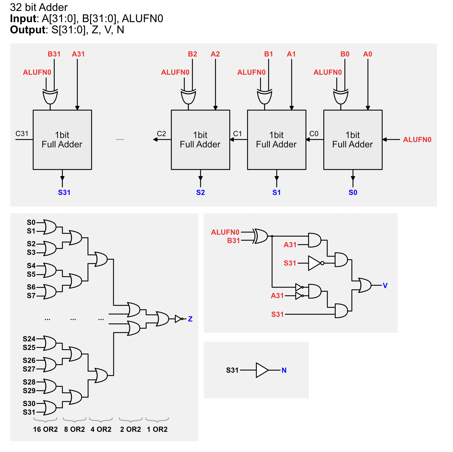
Zwhich is true when the S outputs are all zero (i.e.,NOR(S) == 1 ? Z = 1 : Z = 0)Vwhich is true when the addition operation overflows (i.e., the result is too large to be represented in 32 bits), andNwhich is true when the S is negative (i.e.,S31 == 1 ? N = 1 : N = 0).
The following schematic is a big picture for how to go about the design:
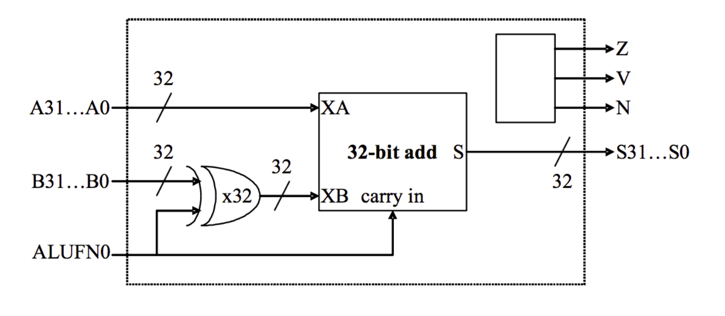
The ALUFN0 input signal selects whether the operation is an ADD or SUBTRACT.
ALUFN0will be set to0for anADD (S = A + B)and1for aSUBTRACT (S = A – B);- To do a
SUBTRACT, the circuit first computes the two’s complement negation of the “B” operand by inverting “B” and then adding one (which can be done by forcing the carry-in of the 32-bit add to be 1).
A[31:0] and B[31:0] are the 32-bit two’s complement (SIGNED) input operands and S[31:0] is the 32-bit output. Z/V/N are the three other output code bits described above.
Start by implementing the 32-bit add using a ripple-carry architecture. You’ll have to construct the 32-input NOR gate required to compute Z using a tree of smaller fan-in gates (the parts library only has gates with up to 4 inputs).
Computing Overflow
Overflow can never occur when the two operands to the addition have different signs. If the two operands have the same sign, then overflow can be detected if the sign of the result differs from the sign of the operands. Note that XA and XB are just the input nodes of the FA drawn in the diagram above.
Think!
Why is
Vcomputed as above? Start by having a small example, let’s say a 4-bit RCA. If we haveA: 0111, andB: 0001, adding both values will result in a positive overflow. The true answer to this should be decimal8. With signed devices, we need 5 bits to represent decimal 8:01000. However since our RCA can only output 4-bits, we have our output as just1000, and this means decimal -8 in a signed 4-bit output. Now think about other possible overflow cases (negative overflow, etc).
Detailed Adder/Subtractor Schematic
Here’s the detailed schematic of the adder. Please label the nodes yourself before describing them in jsim so that you don’t make typos and end up in a debugging nightmare.
Write your answer in the space provided inside lab3_alu_submit.jsim, and include lab3_testadder.jsim header to test your adder32 unit only. You can comment out lab3checkoff.jsim for the time being.
**********************************
**** FA circuit ******************
.subckt FA a b cin s co
* Paste your answer from Lab 2 here
* Replace the gates using stdcell gates instead of your custom gates
* BEGIN ANSWER


* END ANSWER
.ends

**********************************
**** Adder32 circuit *************
.subckt adder32 ALUFN[0] a[31:0] b[31:0] s[31:0] z v n
* BEGIN ANSWER


* END ANSWER
.ends
*********************************
Test
To use the test jig lab3_testadder.jsim:
- Uncomment the
lab3_testadder.jsimfile in the header and comment the rest as such:.include "nominal.jsim" .include "stdcell.jsim" .include "lab3_mult.jsim" .include "lab3_testadder.jsim" * .include "lab3_testcompare.jsim" * .include "lab3_testboolean.jsim" * .include "lab3_testshifter.jsim" * .include "lab3_testmultiply.jsim" * .include "lab3checkoff.jsim" - Do a GATE-level simulation because now we use stdcell library instead of building our own gates using transistor (see Appendix)
- A waveform window showing the
adder32inputs and outputs should appear as such:
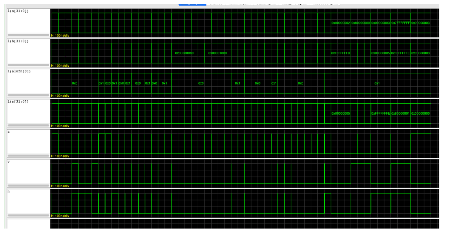
Click the checkoff button (the green tick at the upper right window of JSim). JSim will check your circuit’s results against a list of expected values and report any discrepancies it finds.
Use the waveforms to debug your component if any error is found:
- Find the time when the error occur, and get the value of
aandbandalufn0that caused it - Compute the actual value manually, and check against your
s,z,v, andnvalues - This might give you some clues about which datapath caused the error.
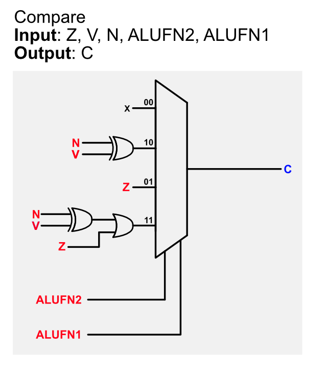
Task 2: Compare Unit
Design a 32-bit compare unit that generates one of two constants (0 or 1) depending on the ALUFN control signals (used to select the comparison to be performed) and the Z, V, and N outputs of the adder/subtractor unit.
Clearly the high order 31 bits of the output are always zero (use that connection to connect 0 in JSim to zero cmp[31:1]). The least significant bit of the output is determined by the answer to the comparison being performed.
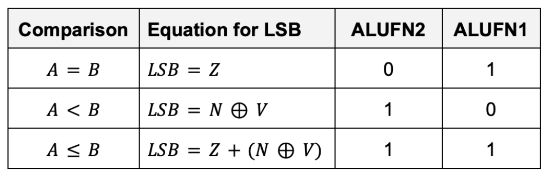
Recall that we control the adder/subtractor unit using ALUFN0 so we cannot use ALUFN0 to control this compare unit too. Therefore, ALUFN[2:1] are used to control the compare unit.
Performance
The Z, V and N inputs to this circuit can only be calculated by the adder/subtractor unit after the 32-bit add is complete. This means they arrive quite late (takes tpd of adder to compute valid ZVN signals) and then require further processing in this module, which in turn makes valid cmp0 shows up after tpd of both adder and compare units.
You can speed things up considerably by thinking about the relative timing of Z, V and N and then designing your logic to minimize delay paths involving late-arriving signals. For instance, if you need to perform computations involving Z and other variables, you can compute those intermediary output involving the other variables first while “waiting” for Z.
Detailed Compare Unit Schematic
Here’s the detailed schematic of the compare unit:
Test
Write your answer in the space provided inside lab3_alu_submit.jsim. We have created a test jig to test your compare unit: lab3_testcompare.jsim. Remember to comment the rest of the test jigs, and only use the compare test jig to test this unit.
.include "nominal.jsim"
.include "stdcell.jsim"
.include "lab3_mult.jsim"
* .include "lab3_testadder.jsim"
.include "lab3_testcompare.jsim"
* .include "lab3_testboolean.jsim"
* .include "lab3_testshifter.jsim"
* .include "lab3_testmultiply.jsim"
* .include "lab3checkoff.jsim"


**********************************
**** Compare32 circuit ***********
.subckt compare32 ALUFN[2:1] z v n cmp[31:0]
* BEGIN ANSWER


* END ANSWER
.ends
**********************************
Task 3: Boolean Unit
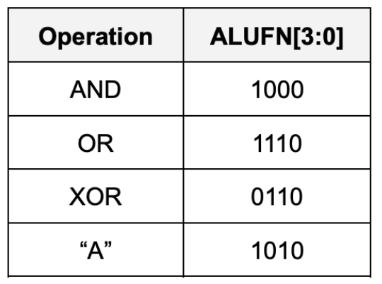
Design a 32-bit Boolean unit for the Beta’s logic operations. One implementation of a 32-bit boolean unit uses a 32 copies of a 4-to-1 multiplexer where ALUFN0, ALUFN1, ALUFN2, and ALUFN3 hardcode the operation to be performed, and Ai and Bi are hooked to the multiplexer SELECT inputs. This implementation can produce any of the 16 2-input Boolean functions; but we will only be using 4 of the possibilities: AND, OR, XOR, and A.
Here’s the general schematic of the Boolean Unit:
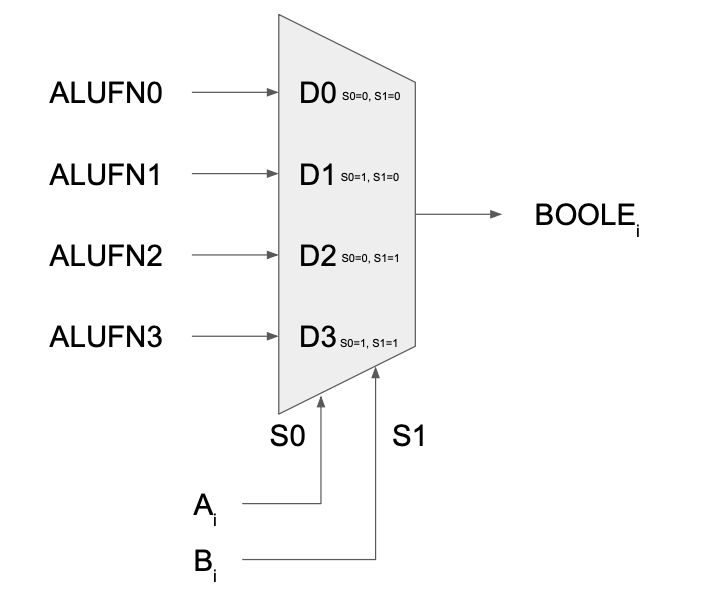
Pay close attention to the ORDER of the multiplexer control signals and its corresponding output. See stdcell documentation on the 4-to-1 mux if you’re unsure how these are obtained.
The following table shows the encodings for the ALUFN[3:0] control signals used by the test jig. If you choose a different implementation you should also include logic to convert the supplied control signals into signals appropriate for your design.
Detailed Boolean Unit Schematic
Here’s the detailed schematic of the Boolean unit:
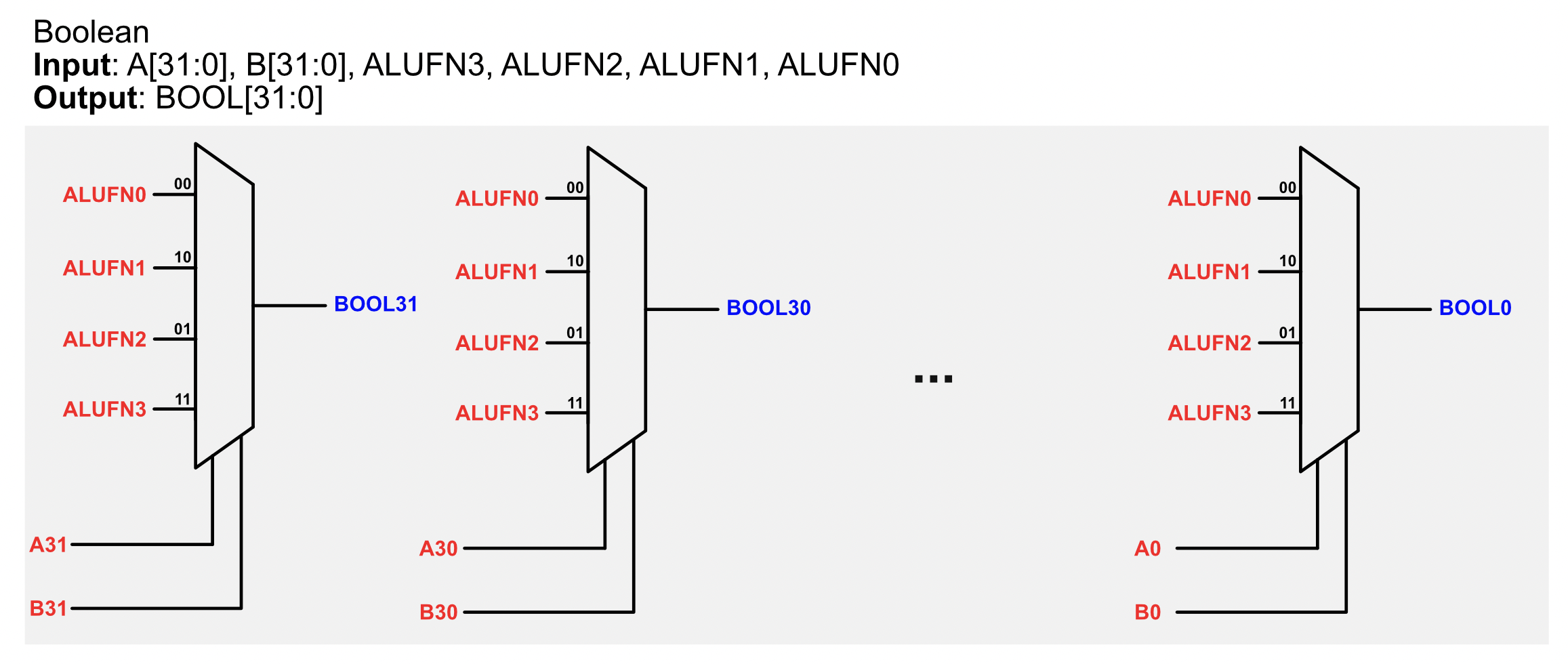
In total, you should utilise 32 4-to-1 multiplexers to build the boolean unit. Please use JSim iterator explained in the appendix for this!
Write your answer in the space provided inside lab3_alu_submit.jsim. We’ve created a test jig to test your boolean unit: lab3_testboolean.jsim. Use it to test that your boolean unit works properly.
.include "nominal.jsim"
.include "stdcell.jsim"
.include "lab3_mult.jsim"
* .include "lab3_testadder.jsim"
* .include "lab3_testcompare.jsim"
.include "lab3_testboolean.jsim"
* .include "lab3_testshifter.jsim"
* .include "lab3_testmultiply.jsim"
* .include "lab3checkoff.jsim"


**********************************
**** Boolean32 circuit ***********
.subckt boole32 ALUFN[3:0] A[31:0] B[31:0] boole[31:0]
* BEGIN ANSWER


* END ANSWER
.ends
**********************************
Task 4: Shifter
Design a 32-bit shifter that implements SRA, SHR and SHL instructions.
- The
A[31:0]input supplies the data to be shifted - The low-order 5 bits of the
B[4:0]are used as the shift count (i.e., from 0 to 31 bits of shift) - We do not use the high 27 bits of the
Binput (meaning thatB[31:5]is ignored in this unit)
For example, if A: 0x0000 00F0 and we would like to shift A to the left by FOUR bits, the B input should be 0x0000 0004
The desired operation will be encoded on ALUFN[1:0] as follows:
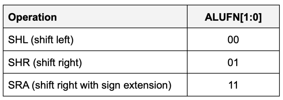
With this encoding, the control signal ALUFN0 is 0 for a left shift (SHL) and 1 for a right shift (SHR) and ALUFN1 controls the sign extension logic on right shift.
- For
SHLandSHR, 0’s are shifted into the vacated bit positions. - For
SRA(“shift right arithmetic”), the vacated bit positions are all filled with A31, the sign bit of the original data so that the result will be the same as dividing the original data by the appropriate power of 2.
Here’s the condensed schematic of the left shifter. In total, you should use 32x5 = 160 2-to-1 multiplexers.
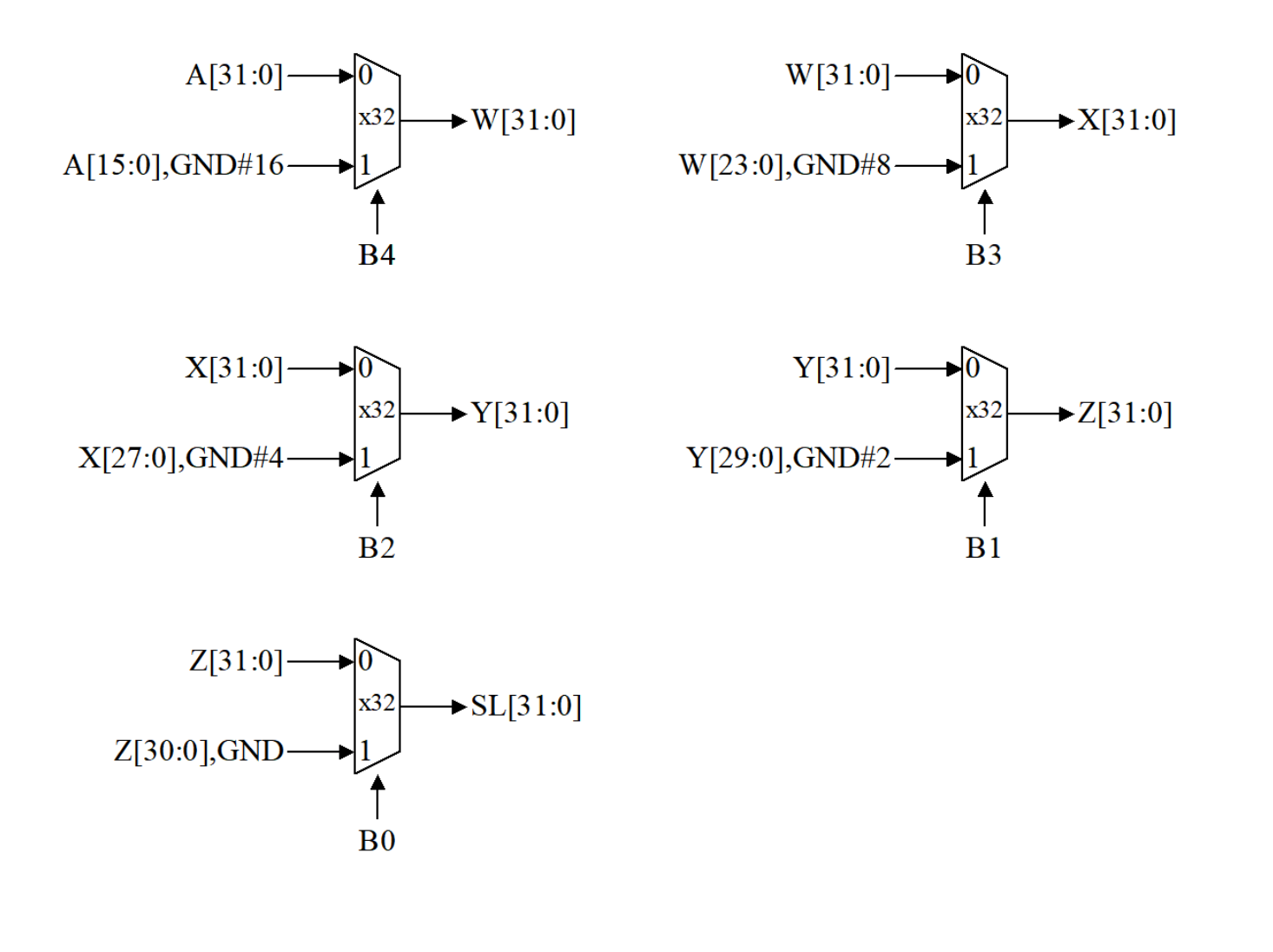
Detailed Shifter Unit Schematic
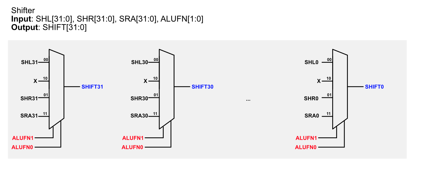
The simplest implementation is to build THREE shifters: one for shifting left, one for shifting right, and one for shifting right arithmetic. Then, we use a 4-way 32-bit multiplexer to select the appropriate answer as the unit’s output.
It’s easy to build a shifter after noticing that a multi-bit shift can be accomplished by cascading shifts by various powers of 2.
- For example, a 13-bit shift can be implemented by a shift of 8, followed by a shift of 4, followed by a shift of 1.
- So the shifter is just a cascade of multiplexers each controlled by one bit of the shift count.
Here’s the detailed schematic of the left shifter. There are really a lot of muxes. Please use the JSim ITERATOR for this!
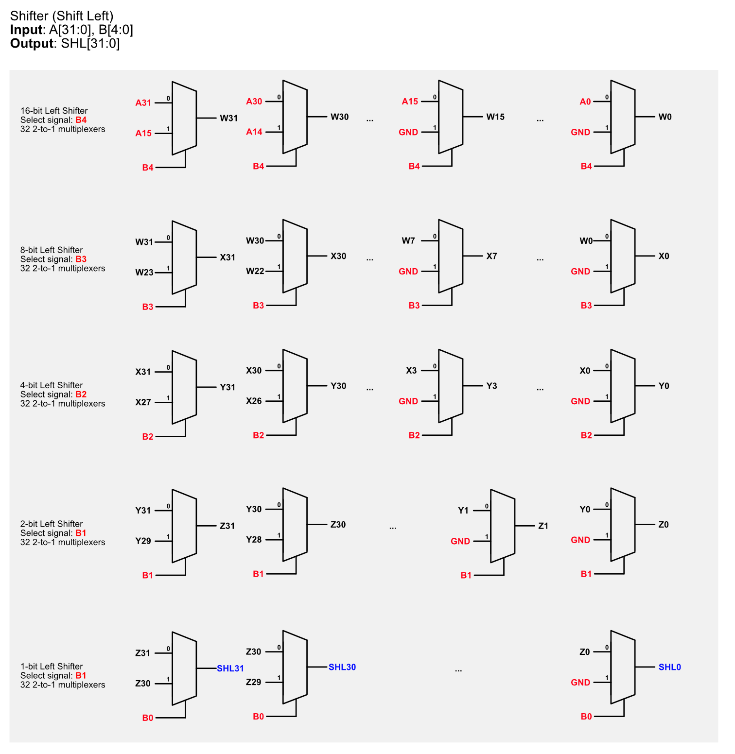
Here’s the detailed schematic of the right shifter.
Here’s the detailed schematic of the right arithmetic shifter.
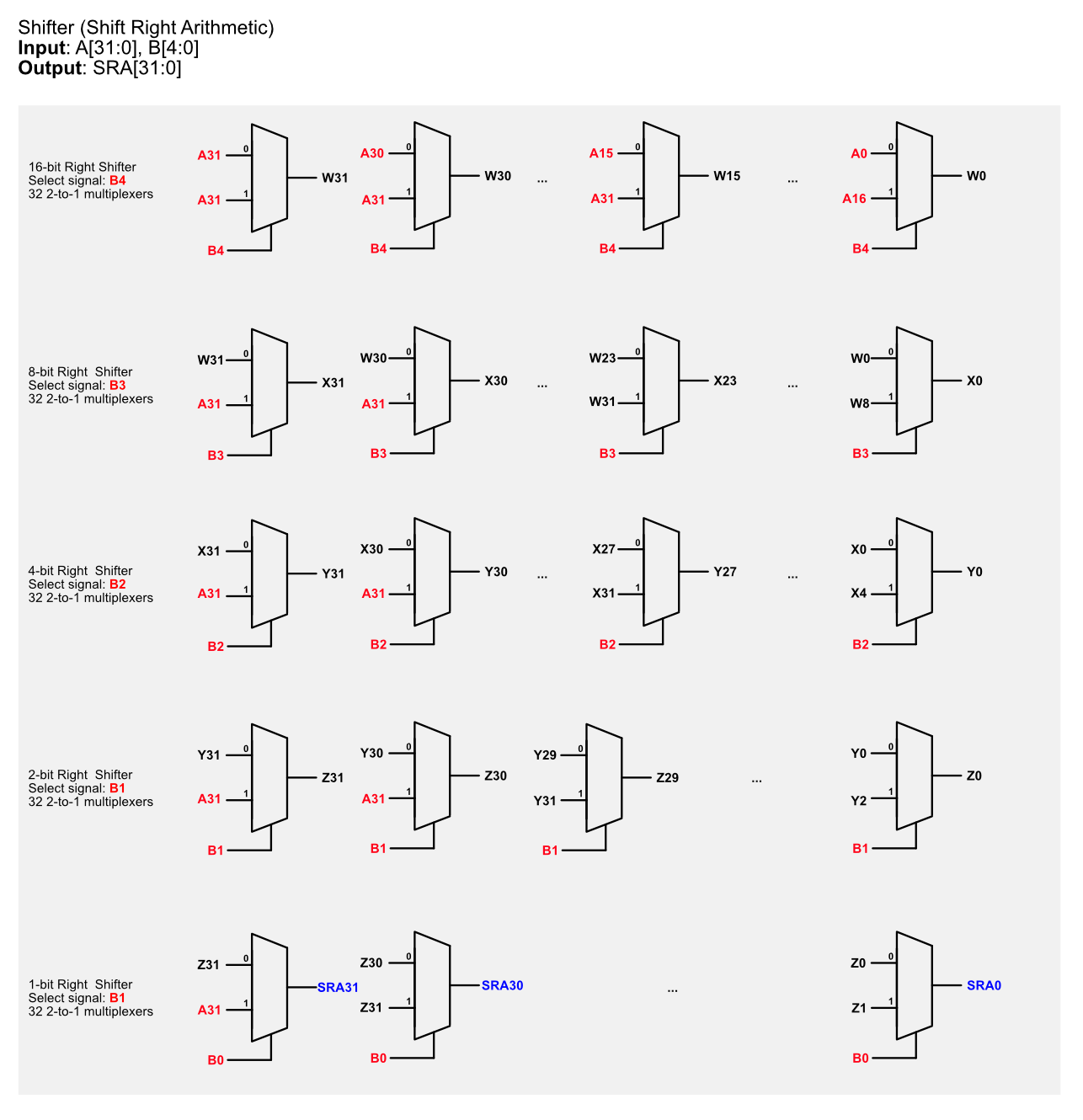
Finally, we can combine all three shifters together to form the total shifter output:
Alternative Approach
Another approach that adds latency but saves gates is to use the left shift logic for both left and right shifts, but for right shifts, reverse the bits of the
Ainput first on the way in and reverse the bits of the output on the way out.
Write your answer in the space provided inside lab3_alu_submit.jsim. We have created a test jig to test your shift unit: lab3_testshifter.jsim. Use it to test that your shifter unit works properly.
.include "nominal.jsim"
.include "stdcell.jsim"
.include "lab3_mult.jsim"
* .include "lab3_testadder.jsim"
* .include "lab3_testcompare.jsim"
* .include "lab3_testboolean.jsim"
 .include "lab3_testshifter.jsim"
* .include "lab3_testmultiply.jsim"
* .include "lab3checkoff.jsim"

**********************************
**** Shifter32 circuit ***********
.subckt shift32 ALUFN[1:0] A[31:0] B[4:0] shift[31:0]
* BEGIN ANSWER


* END ANSWER
.ends
**********************************
Part B: Studying the Multiplier
Open lab3_mult.jsim and realise that this file contains the circuitry for a multiplier unit.
The goal of this section is to study this particular combinational multiplier that accepts 32-bit operands (A, B) and produces a 32-bit output. Multiplying two 32-bit numbers produces a 64-bit product; the result we’re looking for is just the low-order 32-bits of the 64-bit product.
Here is a detailed bit-level description of how a 4-bit by 4-bit unsigned multiplication works. This diagram assumes we only want the low-order 4 bits of the 8-bit product.
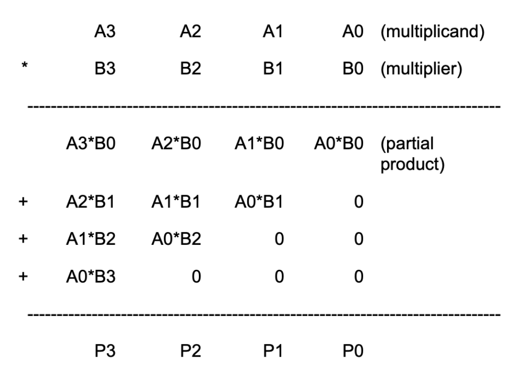
This diagram can be extended in a straightforward way to 32-bit by 32-bit multiplication. Remember that since our machine is only 32-bit, that means we only can store the low-order 32-bits of the result, we don’t need to include the circuitry that generates the rest of the 64-bit product.
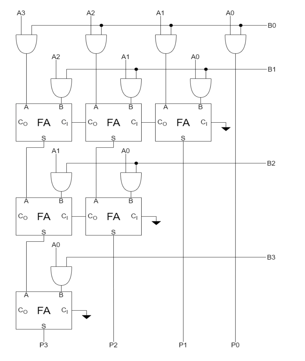
As you can see from the diagram above, forming the partial products is easy. Multiplication of two bits can be implemented using an AND gate. The hard and VERY TEDIOUS part is adding up all the partial products (there will be 32 partial products in your circuit).
- One can use full adders (FAs) hooked up in a ripple-carry configuration to add each partial product to the accumulated sum of the previous partial products (see the diagram below)
- The circuit closely follows the diagram above but omits an FA module if two of its inputs are
0
Multiplier Analysis
The circuit above works with both unsigned operands and signed two’s complement operands. This may seem strange – don’t we have to worry about the most significant bit (MSB) of the operands? With unsigned operands the MSB has a weight of \(2^{MSB}\) (assuming the bits are numbered 0 to MSB) but with signed operands the MSB has a weight of \(-2^{MSB}\).
Doesn’t our circuitry need to take that into account?
It does, but when we are only saving the lower half of the product, the differences don’t appear. The multiplicand (A in the figure above) can be either unsigned or two’s complement (signed), and the FA circuits will perform correctly in either case.
When the multiplier (B in the figure above) is signed, we should subtract the final partial product instead of adding it.
- But subtraction is the same as adding the negative, and the negative of a two’s complement number can be computed by taking its complement and adding 1.
- When we work this through we see that the low-order bit of the partial product is the same whether positive or negated.
- And the low-order bit is ALL that we need when saving only the lower half of the product
If we were building a multiplier that computed the full product, we’d see many differences between a multiplier that handles unsigned operands and one that handles two’s complement (signed) operands, but these differences only affect how the high half of the product is computed.
We’ve provided a test file lab3multiply.jsim to help you study the schematic and output of the multiplier.
This test file includes test cases for:
- all combinations of \((0, 1, -1)*(0,1,-1)\),
- \(2i*1\) for \(i = 0, 1, …, 31\) (positive)
- \(-1*2i\) for \(i = 0, 1, …, 31\) (negative)
- \((3 << i) * 3\) for \(i = 0, 1, …, 31\)
Design Note
Combinational multipliers implemented as described above are pretty slow! There are many design tricks we can use to speed things up – see the appendix on “Computer Arithmetic” in any of the editions of Computer Architecture: A Quantitative Approach by John Hennessy and David Patterson (Morgan Kauffmann publishers).
Part C: Assembling the ALU
Combine the outputs of the finished adder, multiplier (given), compare, boolean and shift units to produce a single ALU output: ALU[31:0]. The simplest approach is to use a 4-way 32-bit multiplexer as shown in the schematic below:
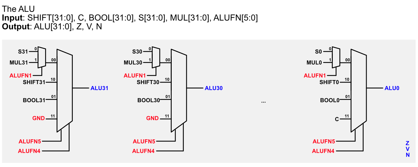
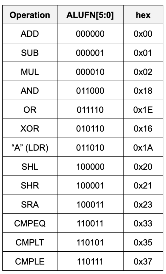
Two additional control signals (ALUFN[5:4]) have been introduced to select which unit will supply the value for the ALU output. The encodings for ALUFN[5:0] used by the test jig lab3checkoff.jsim are shown in the following table:
Note that the Z, V, and N signals from the adder/subtractor unit are included in the terminal list for the alu subcircuit (counted as ALU’s output). You should also have these signals as the ALU output for your 1D Project. While these signals are not needed when using the ALU as part of the Beta, they are included here to make it easier for the test jig to pinpoint problems with your circuit.
Write your answer in the space provided inside lab3_alu_submit.jsim. When you’ve completed your design, you can use lab3checkoff.jsim to test your ALU implementation including the multiplier.
.include "nominal.jsim"
.include "stdcell.jsim"
.include "lab3_mult.jsim"
* .include "lab3_testadder.jsim"
* .include "lab3_testcompare.jsim"
* .include "lab3_testboolean.jsim"
* .include "lab3_testshifter.jsim"
* .include "lab3_testmultiply.jsim"
.include "lab3checkoff.jsim"


**********************************
**** ALU32 circuit ***************
.subckt alu ALUFN[5:0] A[31:0] B[31:0] alu[31:0] z v n
* BEGIN ANSWER


* END ANSWER
.ends
**********************************
When you run the gate-level simulation, you should see the following waveform pops up:
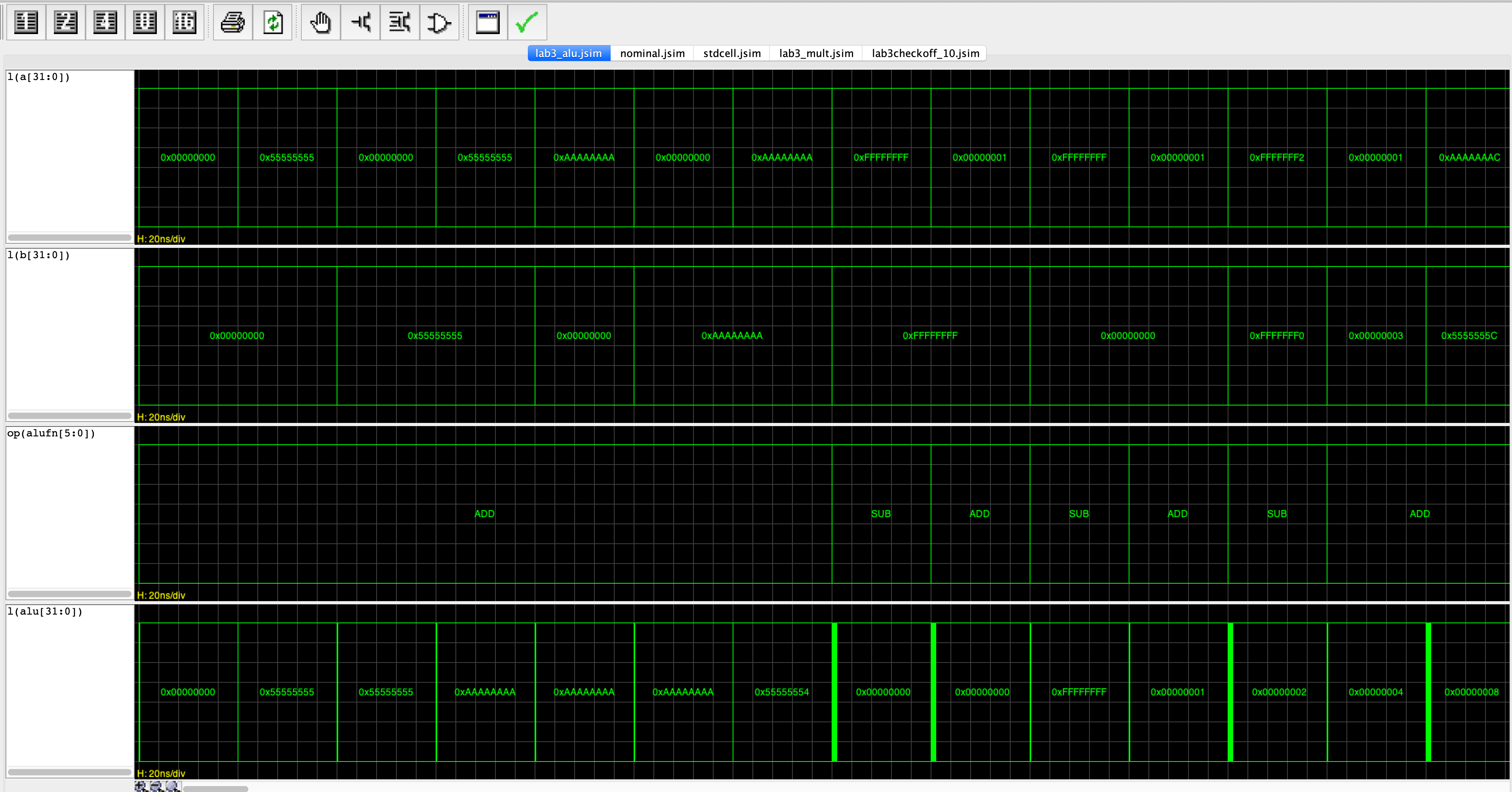
You can use it to debug your alu by finding the opcode that causes the error once you tried to verify (click the tick sign).
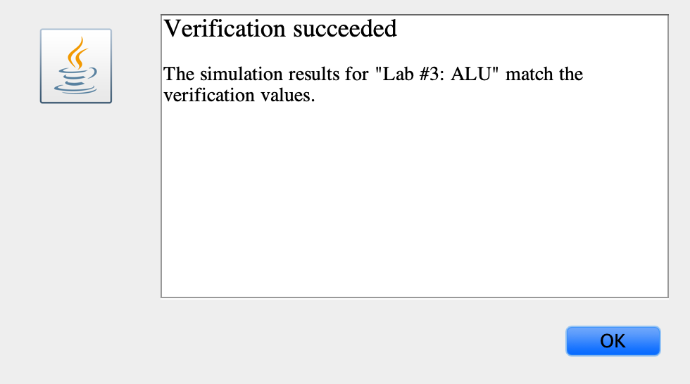
If all expected values are correct, you should see the following window pops up after you click the tick sign and you’ll gain extra happiness:
Appendix: JSim Tricks
Standard Cell Library
The building blocks for our design will be a family of logic gates that are part of a standard cell library, declared for you in the file called stdcell.jsim given in your courseware. You can find its documentation here. The available combinational gates are listed in the table below along with information about their timing, loading and size. You can access the library by starting your netlist with the following include statements:
.include "nominal.jsim"
.include "stdcell.jsim"
We will no longer need to create custom gates from scratch using MOSFET, unlike in our Lab 1 and 2. From now onwards, please build your combinational logic devices using the gates provided in stdcell.jsim.
Gate-level Simulation
Since we are designing at the gate level we can use a faster simulator that only knows about gates and logic values (instead of transistors and voltages). You can run JSim’s gate-level simulator by clicking the GATE button in the JSim toolbar. DO NOT click the transient analysis button anymore.

Note that your design cannot contain any mosfets, resistors, capacitors, etc.; this simulator only supports the gate primitives in the standard cell library.
Inputs are still specified in terms of voltages (to maintain netlist compatibility with the other simulators) but the gate-level simulator converts voltages into one of three possible logic values using the Vil and Vih thresholds specified in nominal.jsim:
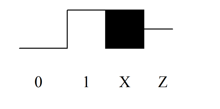
0logic low (voltages less than or equal to VIL threshold)1logic high (voltages greater than or equal to VIH threshold)Xunknown or undefined (voltages between the thresholds, or unknown voltages)Zthe value of nodes that aren’t being driven by any gate output (e.g., the outputs of tristate drivers that aren’t enabled).
The following diagram shows how these values appear on the waveform display:
.connect in JSim
JSim has a control statement that lets you connect two or more nodes together so that they behave as a single electrical node:
.connect node1 node2 node3...
The .connect statement is useful for connecting two terminals of a subcircuit or for connecting nodes directly to ground. For example, the following statement ties nodes cmp1, cmp2, ..., cmp31 directly to the ground node (node 0):
.connect 0 cmp[31:1]
.connect Warning
Note that the .connect control statement in JSim works differently than many people expect: it does NOT connect element-wise For example,
.connect A[5:0] B[5:0]
will connect all twelve nodes (A5, A4, ..., A0, B5, B4, ..., B0) TOGETHER. It is essentially like soldering all 12 pins together, instead of connecting them element-wise. To connect the two buses element-wise, you should use:
.connect A5 B5
.connect A4 B4
.connect A3 B3
.connect A2 B2
.connect A1 B1
.connect A0 B0
Bus unit
The above can be tedious to type. To fix this, you can define a two-terminal device that is used internally, and then use the usual iteration rules (see next section) to make many instances of the device with one X (device) statement:
* declare bus subcircuit
.subckt bus a b
.connect a b
.ends

* use bus subcircuit to connect A and B buses element-wise
X1 A[5:0] B[5:0] bus
To make it convenient for your, there exist the bus unit inside stdcell.jsim that will come in handy to duplicate certain nodes for you with a different name. It is defined as such:
.subckt bus a b
.connect a b
.ends
Therefore if you want to duplicate node a[31:0] into node b[31:0], simply state (position of a and b can be interchangeable, it does not matter):
Xbusab a[31:0] b[31:0] bus
Then you can utilise node b[31:0] afterwards.
JSim Iterators
JSim makes it easy to specify multiple gates with a single "X" statement. You can create multiple instances of a device by supplying some multiple of the number of nodes it expects, e.g., if a device has 3 terminals, supplying 9 nodes will automatically create 3 instances of the device.
For example, a device called xor with 3 terminals: two inputs and one outputs (POSITIONAL ARGUMENT) can be instantiated 3 times in a single instruction as such:
Xtest a[2:0] b[2:0] z[2:0] xor2
is equivalent to:
Xtest#0 a2 b2 z2 xor2
Xtest#1 a1 b1 z1 xor2
Xtest#2 a0 b0 z0 xor2
Iterators can also take the form of prefix[start:stop:step]suffix. For example:
Xtest abc[3:0:2]xyz out[1:0] buffer
is equvilent to:
Xtest#1 abc3xyz out1 buffer
Xtest#2 abc1xyz out0 buffer
Duplicating a signal
There is also a handy way of duplicating a signal. For example, xor-ing a 4-bit bus with a control signal ctl could be written as
Xbusctl in[3:0] ctl#4 out[3:0] xor2
which is equivalent to:
Xbusctl#0 in3 ctl out3 xor2
Xbusctl#1 in2 ctl out2 xor2
Xbusctl#2 in1 ctl out1 xor2
Xbusctl#3 in0 ctl out0 xor2
Connecting Multiple Nodes to ground
Using iterators and the “constant0” device from the standard cell library, here’s a better way of connecting a sample 32-bit bus a[31:0] to ground:
Xgnd a[31:0] constant0
constant0 is a device defined in standard cell library and it has only one terminal (just one input and no output). This is equivalent to:
Xgnd#0 a31 constant0
Xgnd#1 a30 constant0
Xgnd#2 a29 constant0
...
Xgnd#31 a0 constant0
The effect of doing this is that a[31:0] will always give an output of 0 since it is connected to ground. It is a convenient way to zero unused output ports.
Optimising Circuitry
There are many gates that are available in the standard cell library. We can use any gates to synthesize any logic device. However, when designing circuits there are three separate factors that can be optimised:
- Design for maximum performance (minimum latency)
- Design for minimum cost (minimum area)
- Design for the best cost / performance ratio (minimise area times latency)
It is often possible to do all three at once but in some portions of the circuit some sort of design tradeoff will need to be made. When designing your circuitry you should choose which of these three factors is most important to you and optimize your design (use the correct gates) accordingly. You will have to make such design choices in your 2D project.