 50.002 CS
- Related Class Materials
- Introduction to JSim
- User Interface
- Part A: Characterising MOSFETs
- Part B: Noise Immunity
- Part C: Contamination and Propagation delays
- Epilogue
50.002 Computation Structures
Information Systems Technology and Design
Singapore University of Technology and Design
Modified by: Kenny Choo, Natalie Agus, Oka Kurniawan (2021)
Lab 1: CMOS
There’s no code submission for this lab. Simply answer the questionnaire in eDimension Week 2.
Related Class Materials
The lecture notes on Digital Abstraction and CMOS Technology are closely related to this lab.
Task 1 and Task 2: studying the effect of MOSFET “ON” and MOSFET “OFF”.
Related Notes: CMOS Technology
- Types of MOSFETs
- Switching PFET and NFET ON and OFF
- Realise that producing a logic ‘1’ is not always perfect,
- Highly depends on the MOSFET’s conductivity
- An “OFF” MOSFET isn’t always 100% off, there exist leaky current
Task 3 and Task 4: finding optimal VTC
Related Notes: Digital Abstraction
- VTC Section
- Voltage Specifications and Noise Margin
- Realise that we can optimise the noise margin by optimising the MOSFET material
- Understand why static discipline is important, and how we can analyse VTC to choose the best MOSFET design
Task 5: measuring tpd and tcd
Related Notes: CMOS Technology
- Timing Specifications of Combinational Logic Devices
- To analyse the relationship between setup time, hold time, contamination delay, and propagation delays
Introduction to JSim
(you really should’ve read this intro section before coming to class)
In this lab, we will be using a simulation program called JSim, to make measurements of an N-channel MOSFET (or NFET for short). JSim uses mathematical models of circuit elements to make predictions of how a circuit will behave both statically (DC analysis) and dynamically (transient analysis). The model for each circuit element is parameterised, e.g., the MOSFET model includes parameters for the length and width of the MOSFET, as well as many parameters that characterize the physical aspects of the manufacturing process. For the models we are using, the manufacturing parameters have been derived from measurements taken at the integrated circuit fabrication facility, and so the resulting predictions are quite accurate.
The (increasingly) complete JSim documentation can be found here. But we will try to include pertinent information for JSim in each lab writeup.
Download and extract 50002.zip (link can be found our course handout), open it and simply double-click the jsim.jar for this lab. For some newer OS like MacOS Ventura, path to Desktop and Documents may be protected and old Java programs like our jsim and bsim will not even have access to view files in these paths. This means you won’t be able to open the template files. If this happens, you should place the 50002 folder in your home or Downloads directory instead.
User Interface
Open JSim and observe it’s user interface:
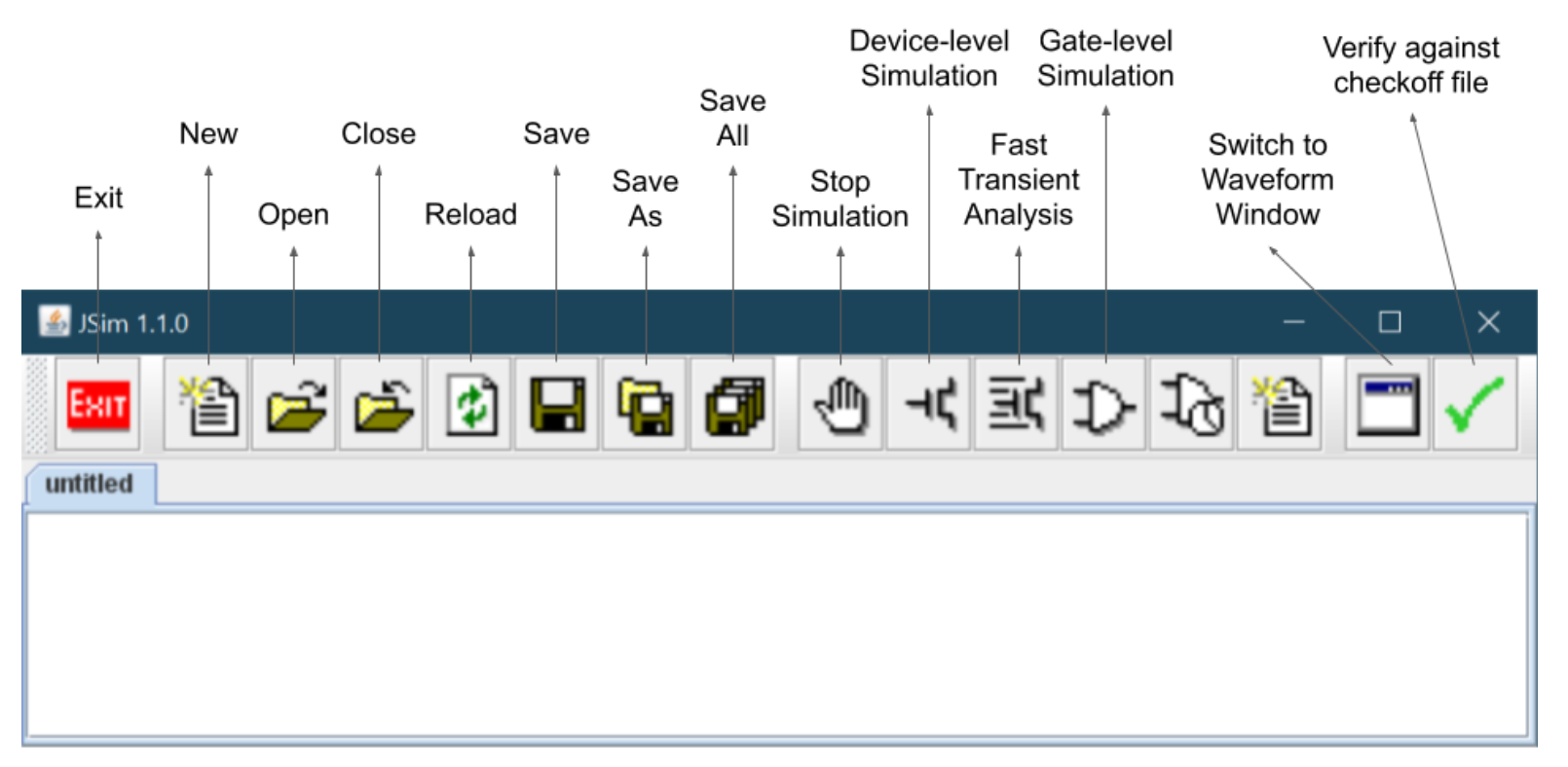
Each icon has the following meaning:
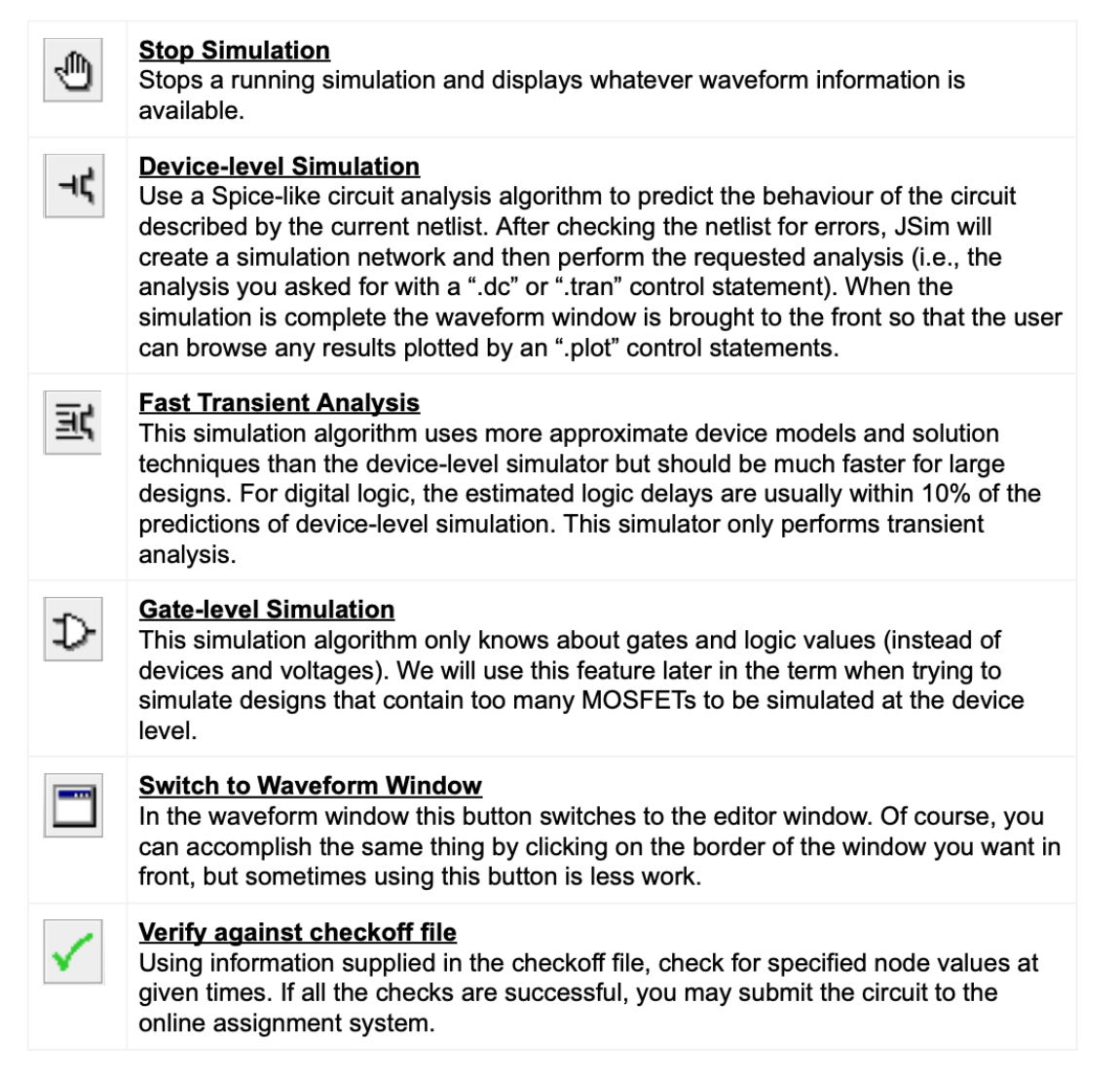
More explanation will be provided as we progress through the lab.
Part A: Characterising MOSFETs
Purpose: Obtain VTC of NFET
Here we to make some measurements of an NFET by hooking it up to a couple of voltage sources to generate different values for VGS and VDS. Our end goal is to obtain the VTC plot of the NFET.
Recall that we learn about VTC in the Digital Abstraction chapter during our lecture.
The setup to characterise our NFET is as follows:
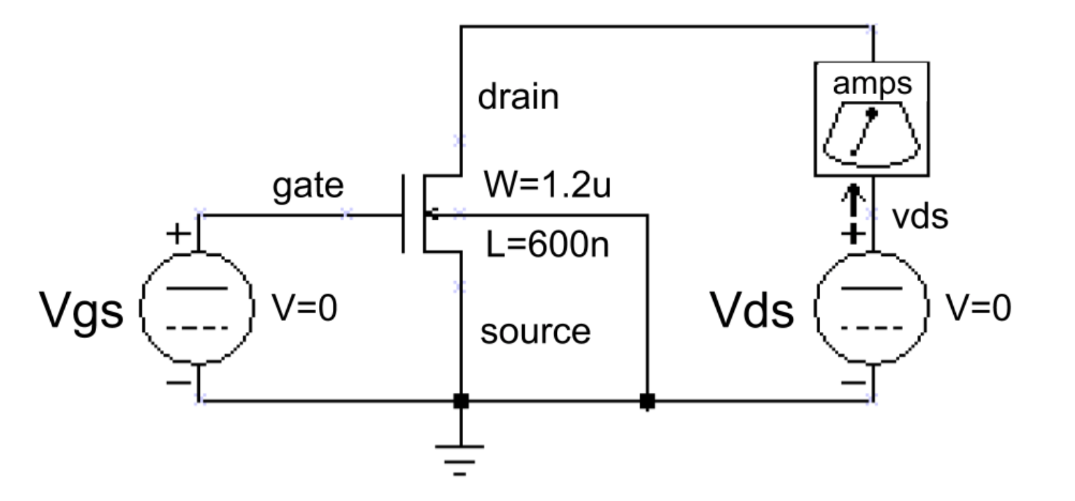
We have included an ammeter (amp built from a 0V voltage source) so we can measure Ids: the current flowing through the MOSFET from its drain (D) terminal to its source (S) terminal. Here’s the translation of the above schematic into our netlist format:
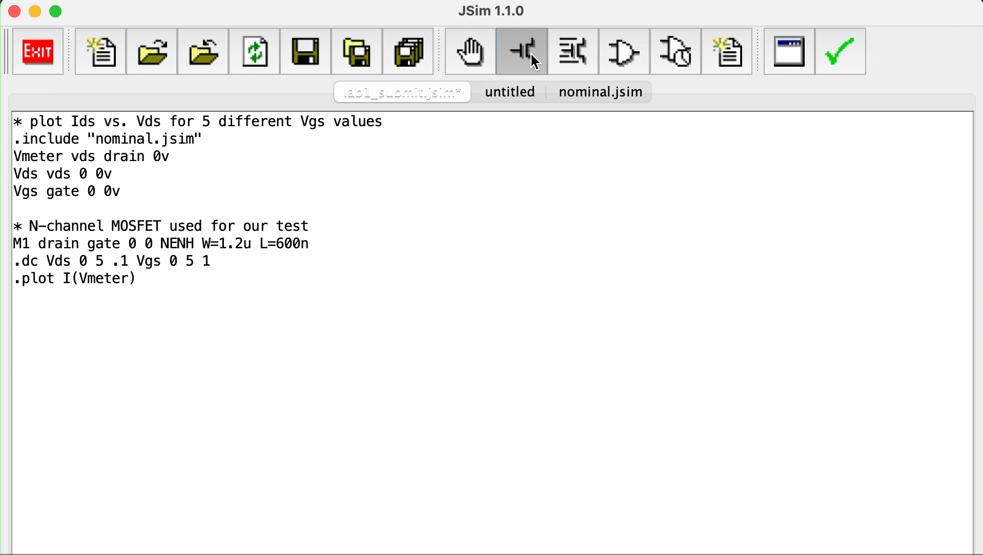
* plot Ids vs. Vds for 5 different Vgs values
.include "nominal.jsim"
Vmeter vds drain 0v
Vds vds 0 0v
Vgs gate 0 0v

* N-channel MOSFET used for our test
M1 drain gate 0 0 NENH W=1.2u L=600n
.dc Vds 0 5 .1 Vgs 0 5 1
.plot I(Vmeter)
Let’s study JSim’s netlist format first before we proceed.
JSim netlist format
The JSim netlist format is quite similar to that used by SPICE, a well-known circuit simulator. Each line of the netlist is one of the following:
- Comment line
- Indicated by an
*(asterisk) as the first character. - Comment and blank lines are ignored when JSim processes your netlist
- C++/Java style comments can also be used
//, all characters starting with this and to the end of the line are ignored./*and*/, any lines or parts of lines enclosed by these are ignored.
- Indicated by an
- Continuation line
- Indicated by a
+as the first character. - Treated as if they had been typed at the end of the previous line (without the
+of course) - No limit to length of an input line, but breaking long lines using
+makes it easier to edit and understand +also continues comment lines
- Indicated by a
- Control statement
- Indicated by
.(period) as the first character. - Provides information about how the circuit is to be simulated
- Indicated by
- Circuit element
- Indicated by a letter as the first character, that represents the type of circuit element. e.g.
rfor resistor,cfor capacitor,mfor MOSFET,vfor voltage source. - Remainder of line specifies which circuit nodes connect to which device terminals and any parameters needed by that type of circuit element. For example, the following line describes a 1000Ω resistor called
R1that connects to nodesAandB:R1 A B 1k
- Indicated by a letter as the first character, that represents the type of circuit element. e.g.
Note
The numbers can be entered using engineering suffixes for readability. Common suffixes are:
- kilo: “k” = 1000
- micro: “u” = 1E-6
- nano: “n” = 1E-9
- pico: “p” = 1E-12
With that knowledge in mind, the code snippet above has the following meaning:
| Line | Description |
|---|---|
| 1, 6 | A comment. Any line that begins with a * signifies a comment. |
| 2 | A control statement that directs JSim to include a netlist file containing the MOSFET model parameters for the manufacturing process we will be targeting this semester. The pathname shown MUST be MODIFIED to point at where your nominal.jsim file is located |
| 3-5 | These specify three voltage sources; each voltage source specifies the two terminal nodes and the voltage we want between them. Note that the reference node for the circuit (marked with a GROUND symbol in the schematic) is always called 0. The v following the voltage specification is not a legal scale factor and will be ignored by JSim–it is included just to remind ourselves that the last number is the voltage of the voltage source. All three sources are initially set to 0 volts but the voltage for the Vds and Vgs sources will be changed later when JSim processes the .dc control statement. We can ask JSim to plot the current through voltage sources which is how we’ll see what Ids is for different values of Vgs and Vds. We could just ask for the current of the Vds voltage source, but the sign would be wrong since JSim uses the convention that positive current flows from the positive to negative terminal of a voltage source. So we introduce a 0V source with its terminals oriented to produce the current sign we’re looking for. |
| 7 | This is the MOSFET. We have described in the following order: drain, gate, source and substrate nodes (in this order!). For instance, MPD1 z a 1 0 NENH sw=8 sl=1 signifies that drain is connected to node z, gate to node a, source to node 1 (this is NOT VDD) bulk to node 0 (ground). The next item names the set of model parameters JSim should use when simulating this device; “NENH” for an NFET, and “PENH” for a p-channel MOFET (PFET). The final two entries specify the width and length of the MOSFET. Note that the dimensions are in microns (1E-6 meters) since we’ve specified the u scale factor as a suffix. Do not forget the u or your MOSFETS will be meters long! You can always use scientific notation (e.g., 1.2E-6) if suffixes are confusing. |
| 8 | A control statement requesting a DC analysis of the circuit made with different settings for the Vds and Vgs voltage sources: the voltage of Vds is swept from 0V to 5V in .1V steps, and the voltage of Vgs is swept from 0V to 5V in 1V steps. Altogether \(51 \times 6\) separate measurements will be made. |
| 9 | A control statement that gets JSim to plot the current through the voltage source named Vmeter. JSim knows how to plot the results from the dual voltage sweep requested on the previous line: it will plot I(Vmeter) versus the voltage of source Vds for each value of voltage of the source Vgs. There will be 6 plots in overall, each consisting of 51 connected data points. |
Waveform Window
After you enter the netlist above, you might want to save your efforts for later use by using the save file button. To run the simulation, click the device-level simulation”button on the toolbar. After a pause, a waveform window will pop up and we can take some measurements.
Controls:
- As you hover the mouse over the waveform window, a moving cursor will be displayed on the first waveform above the mouse’s position and a readout giving the cursor coordinates will appear in the upper left hand corner of the window.
- To measure the delta (difference) between two points, position the mouse so the cursor is on top of the first point.
- Now click left and drag the mouse (i.e., move the mouse while holding its left button down) to bring up a second cursor that you can then position over the second point.
- The readout in the upper left corner will show the coordinates for both cursors and the delta between the two coordinates.
- You can return to one cursor by releasing the left button.
In the example above, we only have one channel. The waveform window shows various waveforms in one or more channels (rows) in general. Initially one channel is displayed for each .plot control statement in your netlist. If more than one waveform is assigned to a channel, the plots are overlaid on top of each using a different drawing color for each waveform. If you want to add a waveform to a channel simply add the appropriate signal name to the list appearing to the left of the waveform display (the name of each signal should be on a separate line).
You can also add the name of the signal you would like displayed to the appropriate .plot statement in your netlist and rerun the simulation. If you simply name a node in your circuit, its voltage is plotted. You can also ask for the current through a voltage source by entering I(Vid).
The waveform window has several other buttons on its toolbar:
Zoom, Pan, Center
You can zoom and pan over the traces in the waveform window using the controls found along the bottom edge of the waveform display. The scrollbar at the bottom of the waveform window can be used to scroll through the waveforms. To recentre the waveform about a particular point, place the cursor at that position and press c.
Task 1: MOSFET “on” Effective Sheet Resistance
To get a sense of how well the channel of a turned-on MOSFET conducts, let us estimate the effective resistance of the channel while the MOSFET is in the linear conduction region. We’ll use the Vgs = 5V curve (the upper-most plot in the window). The equation at the linear region is given by:
The actual effective resistance is given by \(\delta V_{DS}/\delta I_{DS}\) and it clearly depends on which VDS we choose.
Let’s use Vds = 1.2V on the Vgs = 5 curve. We could determine the resistance graphically from the slope of a line tangent to the Ids curve at Vds = 1.2V. But we can get a rough idea of the channel resistance by determining the slope of a line passing through the origin and the point we chose on the Ids curve, i.e., compute channel resistance \(\approx 1.2V / \delta I_{DS}\).
Of course the channel resistance depends on the dimensions of the MOSFET we used to make the measurement.
MOSFET Channel Resistance
For MOSFETs, their Ids is proportional to W/L where W is the width of the MOSFET (1.2 microns in this example) and L is the length (0.6 microns in this example) of the MOSFET. Refer to this notes if you can’t visualise which side is the width and length of the MOSFET.
When reporting the effective channel resistance, it’s useful to report the sheet resistance, i.e., the resistance when W/L = 1. That way you can easily estimate the effective channel resistance for other size devices by scaling the sheet resistance appropriately.
Since W/L = 2 for the device you measured, it conducts twice as much current and has half the channel resistance as a device with W/L = 1, so you need to double the channel resistance you computed above in order to estimate the effective channel sheet resistance.
Record down the value for the effective channel sheet resistance you calculated from that measurement.
Task 2: MOSFET “off” Leakage Current
Now let us see how well the MOSFET turns “off.” We would assume a MOSFET that is “off” should have 0 Ids.
Take some measurements of Ids at various points along the Vgs = 0V curve (the bottom-most plot in the window). Notice that they are not zero!
Subthreshold Conduction
MOSFETs do conduct minute amounts of current even when officially off, a phenomenon called subthreshold conduction. While negligible for most purposes, this current is significant if we are trying to store charge on a capacitor for long periods of time (this is what DRAMs try to do).
Make a measurement of Ids when Vgs = 0V and Vds = 2.5V.
- Based on this measurement report how long it would take for a .05pF capacitor to discharge from 5V to 2.5V, i.e., to change from a valid logic
1to a voltage in the forbidden zone. - Recall from Physics II (10.005) that \(Q = CV\), so we can estimate the discharge time as \(t=C*V/I_{OFF}\).
- So if our MOSFET switch controls access to the storage capacitor, you can see we will need to refresh the capacitor’s charge at fairly frequent intervals.
Record down the estimated discharge time and head to eDimension to answer the related question.
Part B: Noise Immunity
Setup and Introduction
Defining Circuit Elements Using .subckt
Create a new file and name it task_cf.jsim, and paste the following code. The following JSim netlist shows you how to define your own circuit elements using the .subckt statement:
* circuit for Lab#1, Task 3 and 4
.include "nominal.jsim"

* 2-input NAND: inputs are A and B, output is Z
.subckt nand2 a b z
MPD1 z a 1 0 NENH sw=8 sl=1
MPD2 1 b 0 0 NENH sw=8 sl=1
MPU1 z a vdd vdd PENH sw=8 sl=1
MPU2 z b vdd vdd PENH sw=8 sl=1
.ends

* INVERTER: input is A, output is Z
.subckt inv a z
MPD1 z a 0 0 NENH sw=16 sl=1
MPU1 z a vdd vdd PENH sw=16 sl=1
.ends
The .subckt statement introduces a new level of netlist.
- All lines following the
.subcktup to the matching.endsstatement will be treated as a self-contained subcircuit. - This includes model definitions, nested subcircuit definitions, electrical nodes and circuit elements.
- Remember the order of mosfet node declaration: drain gate source substrate(bulk)
MPD1 z a 1 0 NENH sw=8 sl=1signifies that drain is connected to nodez, gate to nodea, source to node1(this is NOT VDD) bulk to node0(ground)- Notice how the source node of MPD1 is connected to the drain node of MPD2, which means that both NFETs are connected in series
- Both PFETs are connected in parallel (by CMOS rule)
The only parts of the subcircuit visible to the outside world are its terminal nodes which are listed following the name of the subcircuit in the .subckt statement:
.subckt name terminals…
* internal circuit elements are listed here
.ends
In the example netlist, two subcircuits are defined:
nand2which has 3 terminals nameda,bandzinside thenand2subcircuitinvwhich has 2 terminals namedaandz
Using Subcircuits
Once the definitions are complete, you can create an instance of a subcircuit using the X circuit element:
Xid nodes… name
where:
name: the name of the circuit definition to be used,id: a UNIQUE name for this instance of the subcircuitnodes…: the names of electrical nodes that will be hooked up to the terminals of the subcircuit instance
There should be the same number of nodes listed in the X statement as there were terminals in the .subckt statement that defined name.
For example, here’s a short netlist that instantiates 3 NAND gates (called g0, g1 and g2):
Xg0 d0 ctl z0 nand2
Xg1 d1 ctl z1 nand2
Xg2 d2 ctl z2 nand2
Explanation:
- The node
ctlconnects to all threenand2gates instances; all the other terminals are connected to different nodes. - Note that any nodes that are private to the subcircuit definition (i.e. nodes used in the subcircuit that don’t appear on the terminal list) will be unique for each instantiation of the subcircuit (like local variables):
- For example, there is a private node named
1used inside thenand2definition. - When JSim processes the three
Xstatements above, it will make three independent nodes calledxg0.1,xg1.1andxg2.1, one for each of the three instances ofnand2. - There is no sharing of internal elements or nodes between multiple instances of the same subcircuit.
- The example netlist above uses
vdd(jsim standard for power source) whenever a connection to the power supply is required.
- For example, there is a private node named
Shared Nodes
There are two common shared nodes in jsim: vdd and 0. Please do not use these to name your custom electrical nodes.
It is sometimes convenient to define nodes that are shared by the entire circuit, including subcircuits; for example, power supply nodes. The ground node 0 is such a node; all references to 0 anywhere in the netlist refer to the same electrical node. The included netlist file nominal.jsim defines another shared node called vdd using the following statements:
.global vdd
VDD vdd 0 3.3v
The example netlist above allows us to use vdd whenever a connection to the power supply is required.
Symbolic Dimensions
The other new twist introduced in the example netlist is the use of symbolic dimensions for the MOSFETs (SW= and SL=) instead of physical dimensions (W= and L=). Symbolic dimensions specify multiples of a parameter called SCALE, which is also defined in nominal.jsim:
.option SCALE=0.6u
So with this scale factor, specifying SW=8 is equivalent to specifying W=4.8u.
Using symbolic dimensions is encouraged since it makes it easier to determine the W/L ratio for a MOSFET (the current through a MOSFET is proportional to W/L) and it makes it easy to move the design to a new manufacturing process that uses different dimensions for its MOSFETs. Note that in almost all instances SL=1 since increasing the channel length of a MOSFET reduces its current carrying capacity, not something we’re usually looking to do.
We’ll need to keep the PN junctions in the source and drain diffusions reverse biased to ensure that the MOSFETs stay electrically isolated, so the substrate terminal of NFET (those specifying the NENH model) should always be hooked to ground (node 0). Similarly the substrate terminal of PFET (those specifying the “PENH” model) should always be hooked to the power supply (node vdd).
Task 3: Optimising Noise Margins
To maximize both noise margins we want to have the transition in the voltage transfer characteristic (VTC) of the nand2 gate centered halfway between ground and the power supply voltage (3.3V)
Think!
Why do we need to “center” the the VTC between
0and3.3V to maximise both noise margins? Review the lecture on digital abstraction.
To determine the VTC for nand2, we’ll perform a dc analysis to plot the gate’s output voltage as a function of the input voltage using the following additional netlist statements. Paste this under the nand2 and inverter declaration you made above in the new file.
* dc analysis to create VTC
Xtest vin vin vout nand2
Vin vin 0 0v

Vol vol 0 0.3v
Voh voh 0 3v

.dc Vin 0 3.3 .005
.plot vin vout voh vol
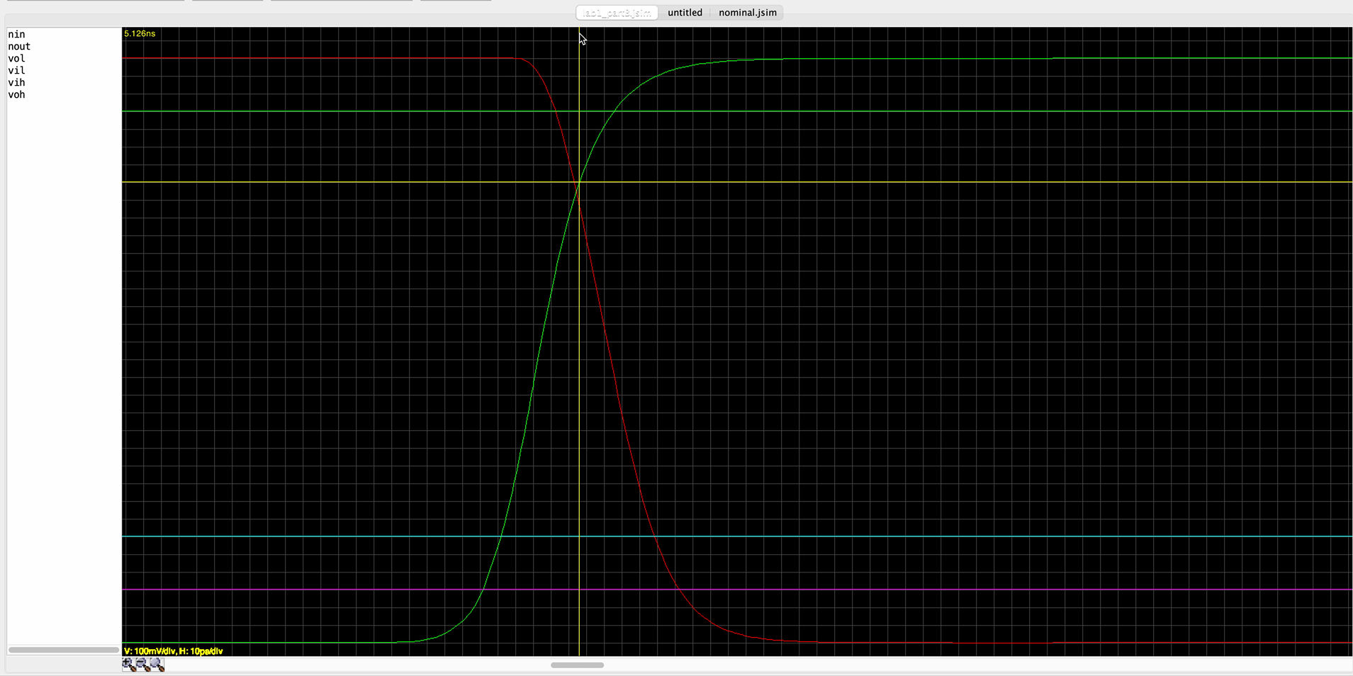
Run the device-level simulation, and the following window should appear:
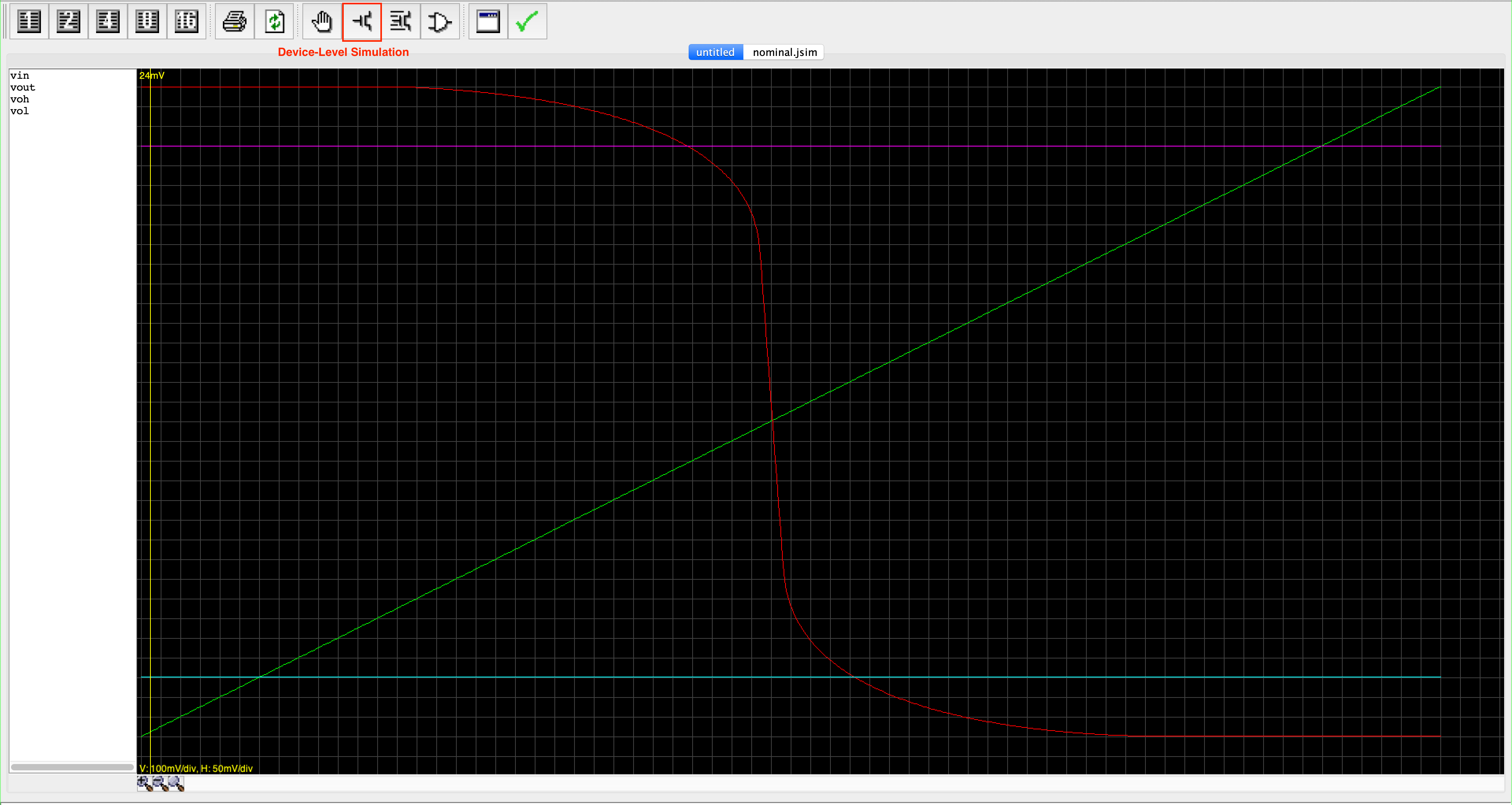
One possible way to center the VTC transition is to adjust the size of the NFET in the nand2 definition as SW=8 SL=1 and adjust the width (SW) of both pFETs until the plots for vin and vout (green and red line) intersect at about 1.65 volts. Keep the SL of the pFETs the same.
- You can also adjust SW, SL of both NFET and PFET as you wish, but we save you that guessing game and give you the most optimal setting right away.
- Just try different integral widths (i.e, 9, 10, 11, …) for the value of
SWof the pFETs in thenand2definition. - Report the integral width that comes closest to having the curves intersect at 1.65V.
Record down the SW value you found and head to eDimension to answer the related question.
Task 4: Finding Noise Immunity
Keep the SW value you found in Task 3 for the rest of this lab!
The noise immunity of a gate is the smaller of the low noise margin (Vil - Vol) and the high noise margin (Voh - Vih). If we specify Vol = 0.3V and Voh = 3.0V, what is the largest possible noise immunity we could specify and still have the “improved” NAND gate of part (C) be a legal member of the logic family?
Record down the noise immunity value and head to eDimension to answer the related question.
Hint:
- To measure the low noise margin, use the VTC to determine what VIN has to be in order for VOUT to be 3V, and then subtract VOL (0.3V) from that number.
- To measure the high noise margin, use the VTC to determine what VIN has to be in order for VOUT to be 0.3V, and then subtract that number from VOH (3.0V).
- We’ve added some voltage sources corresponding to VOL and VOH (which lines of the code was it?) to make it easier to make the measurements on the VTC plot.
Make these measurements using your “improved” nand2 gate that has the centered VTC, i.e., with the updated widths for the PFETS.
Part C: Contamination and Propagation delays
Now that we have the MOSFETs ratioed properly to maximize noise immunity, let’s measure the contamination time (tc) and propagation time (tp) of the nand2 gate.
tcd and tpd
The contamination delay, tcd, for the
nand2gate will be a lower bound for all the tc measurements we make. Similarly, the propagation delay, tpd, for thenand2gate will be an upper bound for all the tP measurements.
Contamination Delay
Recall that the contamination delay is the period of output validity after the inputs have become invalid. We can compute this by first computing two values: tc rise and tc fall and taking the minimum of the two. These two values are the contamination delay in the case where output is transitioning from low to high (rise), or high to low (fall). The name rise or fall depends on whether the output is about to fall or rise.
The statement: “Output remaining at valid 1” means to maintain output voltage value above Voh, while input at valid 1 means to receive input voltage value above Vih. The same applies for valid 0 on both input and output. Revise the lecture on Digital Abstraction if you’re still confused about this concept of valid 0 and 1.
When we fix one of the inputs of the nand2 gates as vdd, we essentially turn our nand2 gates to an inv (inverter). The truth table of an inv is as follows:
| Vin | Vout |
|---|---|
| 0 | 1 |
| 1 | 0 |
Therefore the computation of tc fall and tc rise for inv is:
tc fall can be computed by first setting the input at valid 0, so we have the output at valid 1. Then, we shall increase the input value to eventually no longer be valid 0 (> Vil) and compute the period of time where the output still remains at valid 1 (before eventually falling). The same logic applies for tc rise.
The computation of tc fall and tc rise is not the same for all gates. For instance, the computation for the two values for a buffer is:
Ensure you understand how the formulas above are derived before proceeding.
Propagation Delay
Similarly, the propagation delay is the period of output invalidity after the inputs have become valid. We can compute this by first computing two values: tp rise and tp fall and taking the maximum of the two. These two values are the propagation delay in the case where output is transitioning from low to high (rise), or high to low (fall). The name rise or fall depends on whether the output is about to fall or rise.
Therefore the computation of tp fall and tp rise for our nand2 gate turned as an inv is:
Following standard practice, we’ll choose the logic thresholds as follows:
- Vol = 10% of power supply voltage = .3
- Vil = 20% of power supply voltage = .6
- Vih = 80% of power supply voltage = 2.6
- Voh = 90% of power supply voltage = 3V
Review the lecture on CMOS Technology to refresh your understanding on propagation delay and contamination delay. This is VERY important especially for Week 3 materials.
Generating test signal
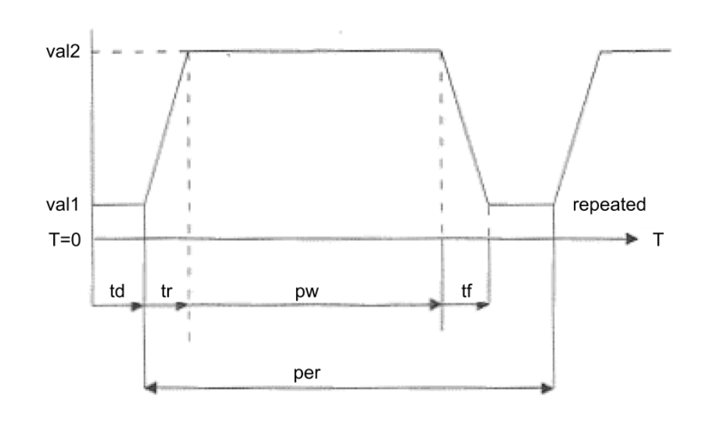
The final thing that we have to prepare to plot a VTC is to generate a test signal. You can use a voltage source with either a pulse or piecewise linear waveform to generate test signals for your circuit. Here’s how to enter the test signal in your netlist:
Vid output 0 pulse(val1 val2 td tr tf pw per)
This statement produces a periodic waveform with the following shape:
Task 5: Measuring tpd and tcd
Replace the netlist fragment from Task 3 with the following test circuit that will let us measure various delays:
* test jig for measuring tcd and tpd
Xdriver vin nin inv
Xtest vdd nin nout nand2
Cload nout 0 .02pf
Vin vin 0 pulse(3.3,0,5ns,.1ns,.1ns,4.8ns)

Vol vol 0 0.3v   // make measurements easier!
Vil vil 0 0.6v
Vih vih 0 2.6v
Voh voh 0 3.0v

.tran 15ns
.plot vin
.plot nin nout vol vil vih voh
Make these measurements using your “improved” nand2 gate from Task 3 that has the centered VTC, i.e., with the updated widths for the PFETs.
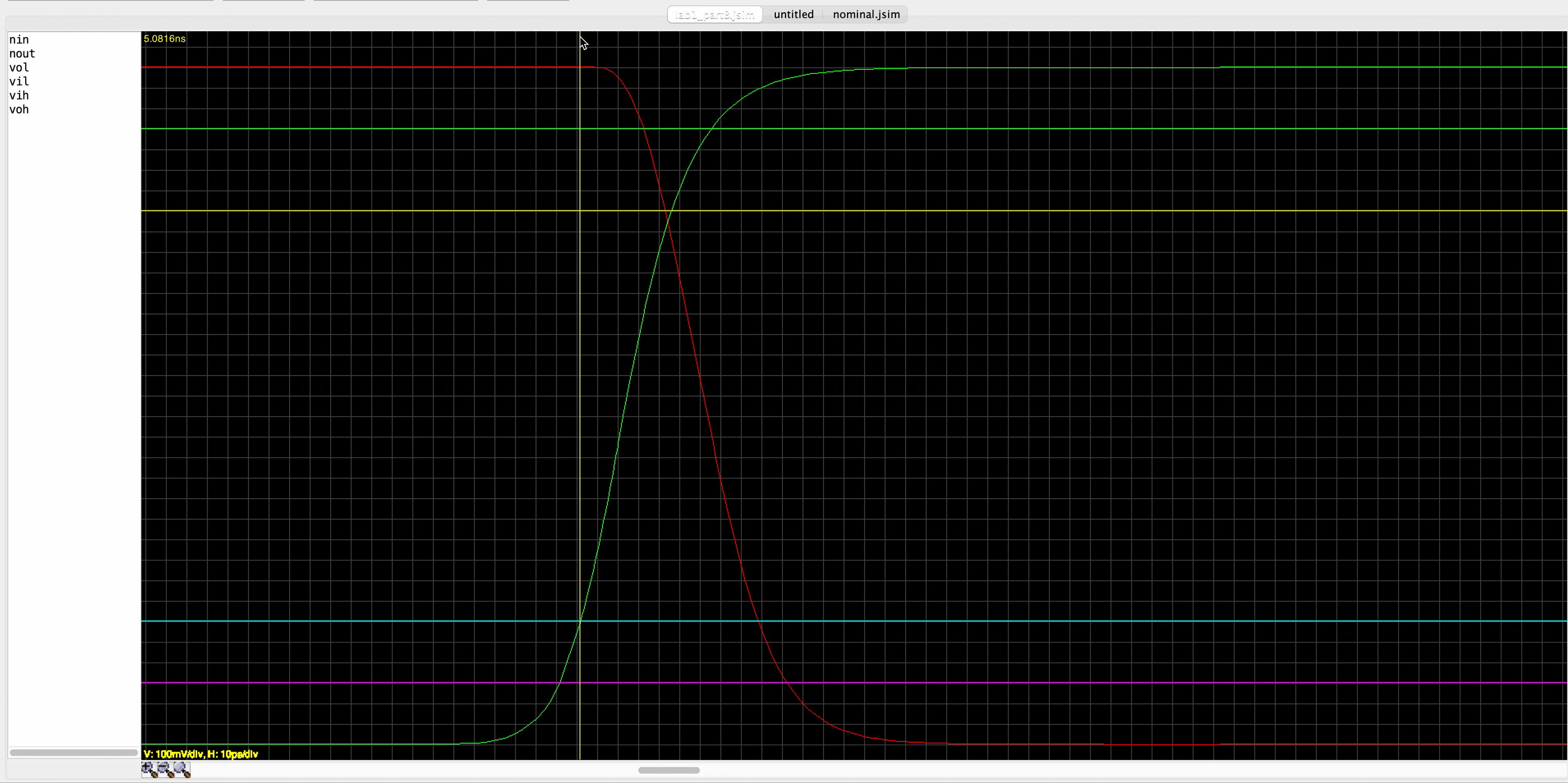
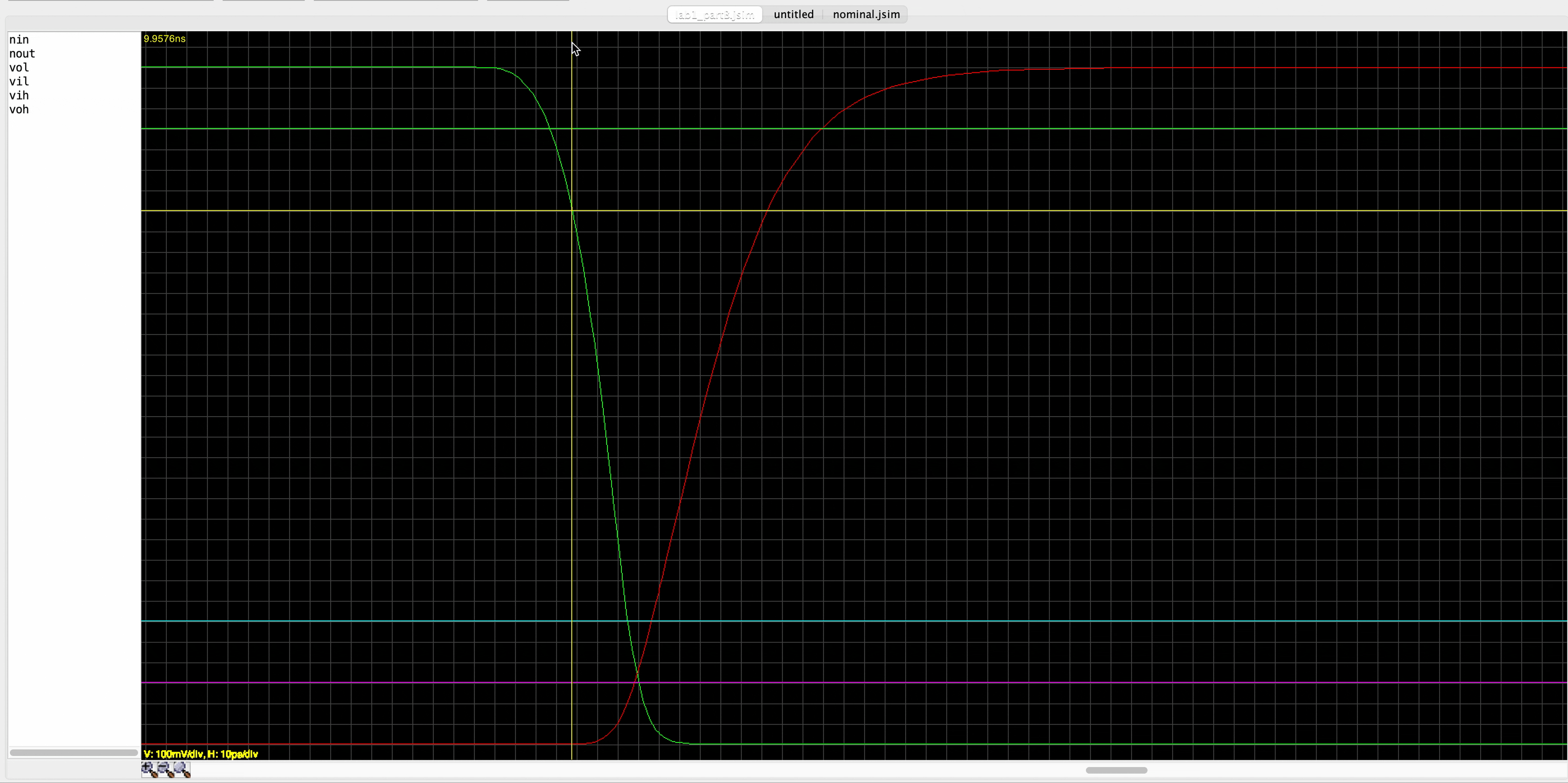
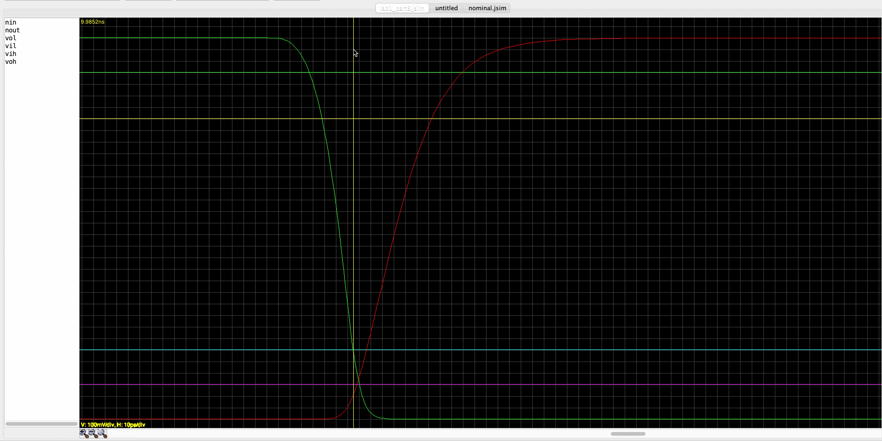
We use an inverter (inv) to drive the nand2 input since we would normally expect the test gate to be driven by the output of another gate (there are some subtle timing effects that we’ll miss if we drive the input directly with a voltage source). Run the simulation with the “device-level simulation” button and measure the contamination and propagation delays for both the rising and falling output transitions. You will meet such waveforms:
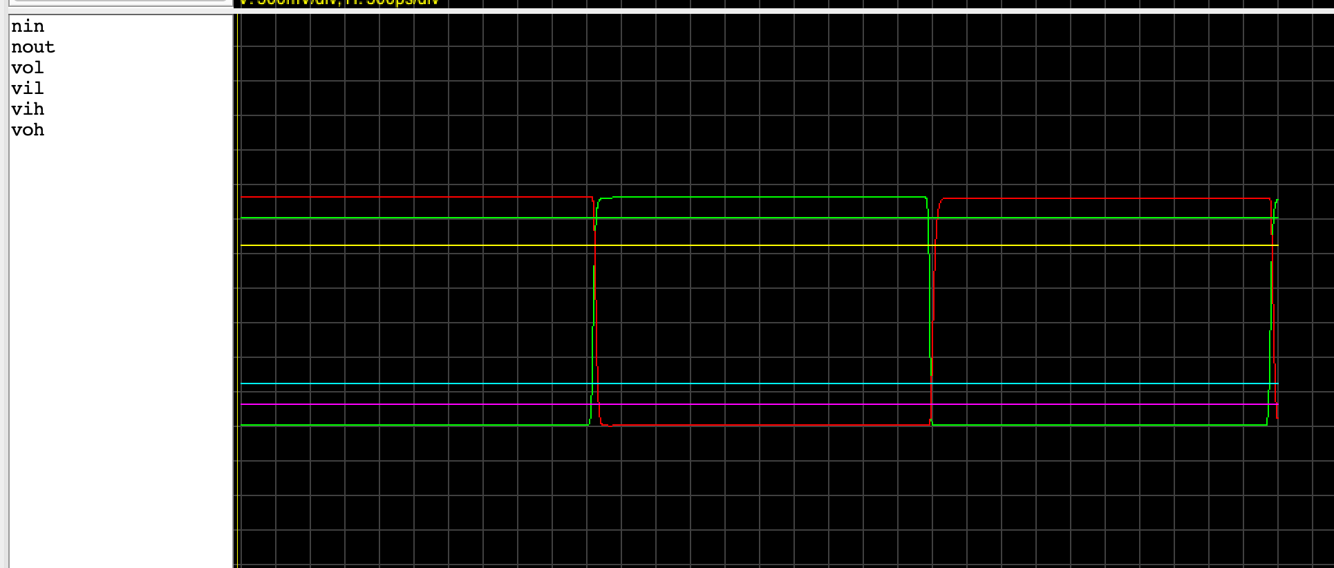
You will need to zoom in on the transitions in order to make an accurate measurement. Combine your answers for tc rise, tc fall, tp rise, and tp fall as described above to produce estimates for tcd and tpd.
Measure tc fall
Zoom in to a section where the output signal (red) is falling (conversely when the input green signal is rising). Note the four horizontal lines are helper lines for voh, vih, vil, and vol (top to bottom).
Click on the start time when the input has just turned invalid: crossed the teal horizontal line (vil), and drag to the end time where the red graph just crossed the green horizontal line (voh). On the top left hand corner in jsim, find the time difference (in white) between the two points. This will be your tc fall value.
Please understand why we compute tc fall this way and don’t just blindly follow the instructions.
Measure tc rise
Similarly, here’s where you can compute tc rise.
Measure tp fall
To measure tp fall, your time measurement should start from the moment the input becomes valid (crosses the yellow horizontal line vih) to the moment the output becomes valid (crosses the purple horizontal line vol).
Measure tp rise
The same ordeal as tp fall, but in the section where the output is rising:
Compute tpd and tcd
Reporting overall device tpd and tcd
As said above, to compute overall device tpd, we take the maximum between tp rise and tp fall. To compute its tcd, we take the minimum between tc rise and tc fall.
The why should be pretty intuitive by now. tcd can be seen as the memory ability of the device; indicating how long it is able to produce the previous valid output even when the input has currently turned invalid. If your device remembers rising case better than falling case, the overall memory ability that should be reported for the device should be the smaller of the two.
Likewise, tpd is some sort of loading time of the device. If your device loads longer in the falling case than the rising case, we have to report the longer loading time so our users know how to mitigate that. In short, we need to take into account that the device will be used to produce both rising and falling cases.
Record down the contamination tcd and propagation tpd delays for both the rising and falling output transitions and fill in the respective questions on eDimension. Please zoom in at least 4-5 times before doing this to get a clearer picture of the signals.
Epilogue
For many consumer products, designs are tested in the range of 0°C to 100°C. We can have JSim simulate our test circuit at a different temperature by adding a .temp control statement to the netlist. Normally JSim simulates the circuit at room temperature (25°C), but we can simulate the circuit at, say, 100°C by adding the following code to our netlist:
.temp 100
Think!
Do you think the values of tcd will increase at 100°C? What about the values of tcd?
If for example, we have the following measurements:
- At 25°C, tcd = 0.1ns and tpd = 0.2ns
- At 100°C, tcd = 0.25ns and tpd = 0.3ns
Which values, at 25°C or 100°C will you use to record the device tpd specs? What about for tcd?
If a 2019 Intel Core i9 processor is rated to run correctly at 2.3 GHz at 100°C, how many % more can you clock it (faster) and still have it run correctly at room temperature (assuming tpd is the parameter that determines “correct” computer behavior)? This is why you can usually get away with overclocking your CPU—it’s been rated for operation under much more severe environmental conditions than you’re probably running it at!