 50.002 CS
- Introduction
- The Counter Game
- Planning the Datapath
- Designing the
REGFILE - Designing the ALU and Support Datapath
- Designing the Control Logic
- The Complete Datapath
- Summary
50.002 Computation Structures
Information Systems Technology and Design
Singapore University of Technology and Design
Natalie Agus (Fall 2020)
Designing a Programmable Datapath
For your 1D project (pre 2025), you are required to build an electronic game prototype that utilizes a 16-bit ALU. You can do this by first designing a programmable datapath and the control logic (FSM) for your game, and finally implement on your FPGA.
This document shows an example on how you can create a programmable data path for a simple game idea called the Counter Game. The complete code can be found in this repository if you’d like to dive straight to it. Otherwise, read along.
Introduction
When you brainstorm for a game, try to keep two very important things in mind:
- Ideation: A good game doesn’t have to be complicated. It can be a very simple math-based game, or strategy game. You can find inspiration using simple arcade games in the 1990s.
- Think about the external I/O devices that you have to manage.
Selecting I/O Devices
A recommended route is simply a bunch of buttons for input (you can get nice, arcade game type buttons online) and small coloured LEDs, or 7 segments as output. You won’t be penalised even if you go for this simple route.
Some Upgrade: Bigger Buttons and RGB LEDs
You can buy bigger buttons, LEDs or 7 segments, and buy transistors (simple, cheap BJT ones) to be used as amplifiers using external power source if the voltage from the Au is not strong enough.
More Upgrade: LED Strips
You can buy LED strips (e.g: WS2812B), and read the specifications: typically the type of serial data and clock cycles required to set the lights. The specification of the model that you buy must be CLEAR, complete with details on how to encode information to light up your LEDs. See this datasheet for WS2812B. You can find a sample driver code for this model here.
Even More Upgrade: LED Dotmatrix, LED Matrix
You can buy LED matrix if you’re confident with your Lucid skills. There are TWO types: a simple up to 8x8 dot matrix,

Or, a bigger bit-addressable matrix like this (e.g; Adafruit matrix LED),

For the dotmatrix, you can use easy registers / dff to manage the data. For the big matrix, you need to use some kind of RAM module (you can use simple RAM default component in Alchitry) to store your data for the matrix to display at all times. You can find a sample driver code for the bit-addressable matrix (Adafruit LED matrix or equivalent) here.
NEVER use dff for massive storage of data to be read by the big matrix! Your compile time is going to take a bizarrely long time or fail altogether because the FPGA does not have enough logic unit!
Beastly upgrade: To use VGA + screen output and USB gamepads.
This is not recommended unless you have had prior experience.
If you’re new to this, then it will waste a lot of your time, and it is very risky with little value-add to your project because the focus of this project is to design a programmable data path, and not to produce a fancy output per se. Note that we also will not entertain any request to teach how to use the VGA output or read USB input. We will prioritise other more important requests instead. If you choose to go down this path, you are on your own.
Just make it work
Again, it will absolutely not affect your grades no matter which I/O devices you choose as long as you are able to create a fun project with neat datapath.
The Counter Game
As an example, let’s assume we were to implement this game called The Counter Game. We have the following elements to our game.
Players: Imagine two players, A and B, competing with one another
Background: They can view a display that shows a number, initially set to 0. The number is increased at a random, varying rate.
Procedure: Any player can choose to collect the number, therefore resetting the number to zero and obtain a score equivalent to the current number when the player choose to collect it. Each player however, can only choose to collect the number three times at maximum. The game runs for 30 seconds, and ends once the timer runs out, or that both players have used up their 3 collection chances.
Winning Condition: The player with the most score at the end of 30 seconds wins the game. If both players end up with the same score, then the game ends in a draw.
I/O Required
Therefore the external inputs required for this game are simply TWO buttons, one for each player.
The external outputs required for this game:
- A 4-digit 7-segment display to show the current collectible number
- A 2-digit 7-segment display to show how much of the 30-seconds time remains, OR simply 5 LEDs placed in a row to display the number of seconds remaining in binary form.
- Two 4-digit 7-segment displays to display the current score of each player, OR simply again a few LEDs placed in a row to display each player’s score in binary.
As stated above, if you were to use a large 7-segment display then purchase some BJT transistors to amplify the power to be high enough e.g: 6V/10V to run the displays.
Planning the Datapath
It is recommended that you follow a generic simplified custom \(\beta\)-like structure (without the PC and RAM unless you want to design a generic instruction set):
- You have a REGFILE system, where it stores a bunch of registers inside that’s addressable. It’s up to you to define how many combinational read ports and how many sequential write ports.
- Combinational Logic Unit: You must utilize a 16-bit ALU (pre 2025), so you have no choice on this. Therefore this makes your datapath to be a 16-bit architecture by default. <>
- You have a Control Unit, which is simply an FSM that gives out different control signals at various time step.
It is imperative that ALL sequential parts that requires CLK is fed with the SAME default Alchitry CLK at 100MHz. You can create other submodules to be plugged into your datapath to act as frequency divider (slowing down the clock cycle) but DO NOT MESS with the CLK for the REGFILE and FSM unless you are a very experienced FPGA developer. <>
Designing the REGFILE
The first step in designing a datapath is to think about how much storage you will need, and how many bits of data your machine can support at each cycle?
Since we are using a 16-bit ALU, it automatically makes your custom game machine a 16-bit architecture. So we shall choose to use 16-bit registers.
For this simple game, we need the following values to be stored:
- Score of P1
- Score of P2
- Number of times P1 has clicked its button
- Number of times P2 has clicked its button
- Current collectible number (counter)
- Seconds (time) left for the game
We also need some registers to act as temporary storage value. Therefore the simplest step is to design a REGFILE unit that contains 16 16-bit registers (4-bit addressable). We can set some register addresses to be fixed:
- 0x0 : P1 Score Reg
- 0x1 : P2 Score Reg
- 0x2 : P1 Button Count Reg
- 0x3 : P2 Button Count Reg
- 0x7 : Current Counter Reg
- 0x8 : Timer Reg
- 0x9 to 0xF : Temp Regs
One possible REGFILE schematic for your custom game datapath is as such:

It is very important to plan the schematic first BEFORE actually coding it on your FPGA. This speeds up your development time and save you from the pain of debugging.
In general, a REGFILE system MUST have combinational read ports and sequential write ports. It is up to you to decide how many ports for each. This affect the amount of input and output terminals you need to make to your regfile.
For each read port:
- You need to specify a read address
Rx. Number of bits of register address depend on how many dffs are there in the REGFILE. - Specify a data out port:
Rx_data. Number of bits depend on the number of bits each dff can store.
For each write port:
- You need to specify a write address
Rx. Again, number of bits of register address depend on how many dffs are there in the REGFILE. - A write enable:
WE_Rxsignal, to enable or disable write to this registerRx - Specify a data write in port:
Rx_writedata. Number of bits depend on the number of bits each dff can store.
For this example, we follow the \(\beta\): to have 2 read ports and 1 write ports. Three addresses should be received by the REGFILE: Ra and Rb for read addresses and Rc for write addresses.
- Input:
CLK(obviously!)- 1
WEsignal - 1
Write Addressport (4-bits) - 1
Write Dataport (16-bits) - 2
Read Addressesport (4-bits each)
- Output:
- 2 data out ports:
Ra_dataandRb_data(16 bits each) - DIRECT connection to external output device as a design choice, for convenience (16 bits each):
- Value of
Reg[0x0]to display P1 Score at all times - Value of
Reg[0x1]to display P2 Score at all times - Value of
Reg[0x8]to display game time left at all times
- Value of
- 2 data out ports:
Depending on your design, you may not we need to show the counter value, but it will cause you to keep track of two counters: the one displayed to the players, and this internal counter. These two counter values must be equal at all times. If you have problems synchronising between the two, then just have ONE dff to track the current counter value that’s read by the output device as well similar to how P1 score and P2 score are also displayed.
Coding a REGFILE on an FPGA is not an issue after you have a clear idea about its addressing system, and input/output ports of the module. This REGFILE should be implemented as a single file, e.g: regfile.luc. See this github file for its sample implementation.
Designing the ALU and Support Datapath
We can easily adapt the design of \(\beta\) when we want to connect the ALU with the REGFILE. It is an art to design a good, programmable datapath.
A super simple support datapath should have some kind of ASEL MUX, BSEL MUX, and WDSEL MUX:
ASEL: to decide what’s fed into theAport of the ALUBSEL: to decide what’s fed into theBport of the ALUWDSEL: to decide what’s fed into theDATA INport of the REGFILE (what’s written intoReg[Rc]if any).
The figure below illustrates that:
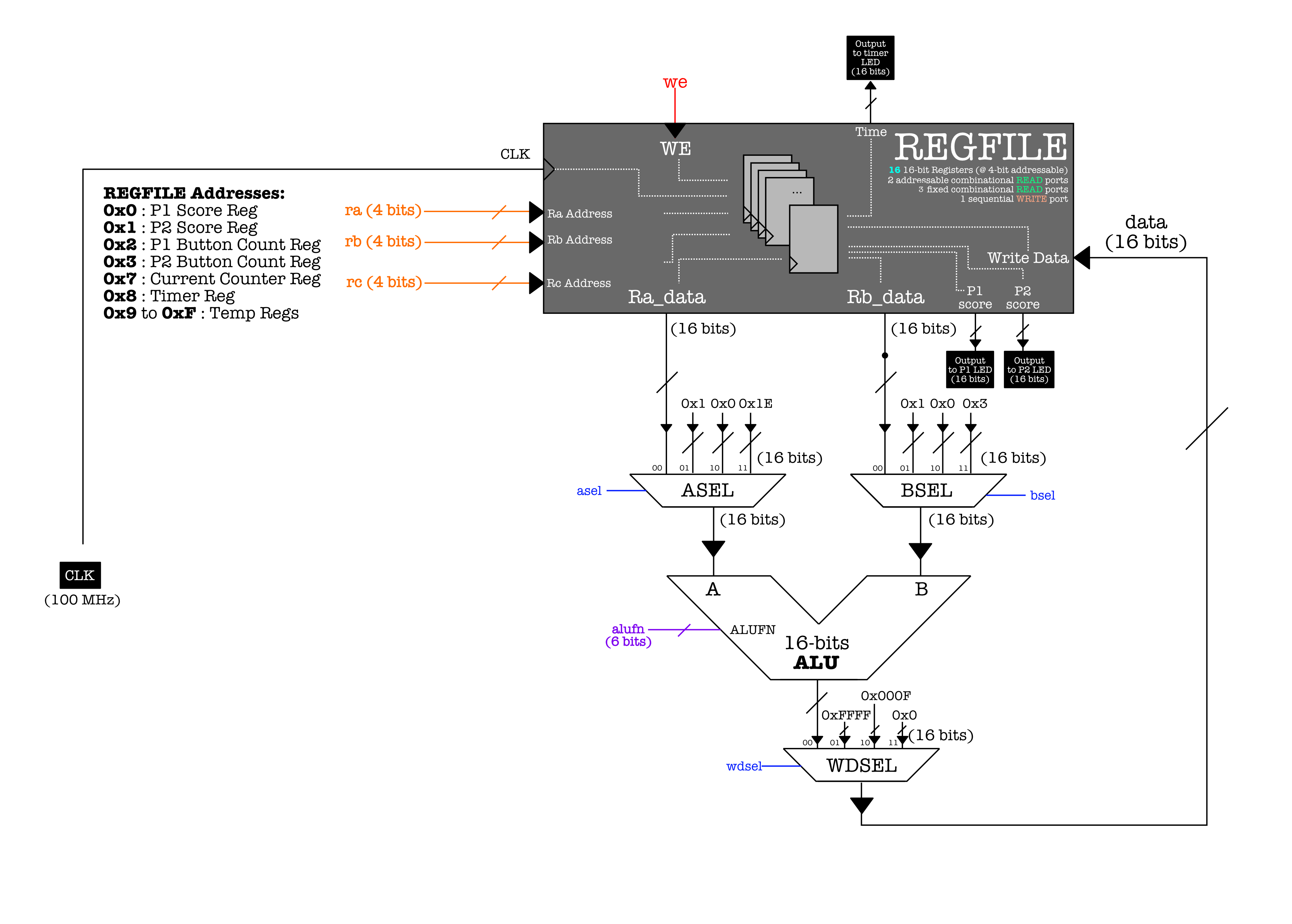
Obviously the control signals required are (coloured in the figure above):
ASELselectorBSELselectorWDSELselectorALUFNto define ALU operationRa, Rb, Rcregister addressesWEfor write enable in REGFILE
Design Considerations
We can choose to expand the inputs to ASEL/BSEL/WDSEL MUXes that best suit our game.
How many inputs should ASEL/BSEL/WDSEL MUX handle? This affects how many bits the control signals should be.
- The source of inputs to each MUX can either be from other registers, or other combinational logic units, or a constant that’s relevant for your game.
For this game, we need a few constants and so we hardcode it as inputs to ASEL and BSEL MUXes:
- The value “30” to reset the timer:
0x1Eat theASELMUX - The value “3” to compare against current player’s button press:
0x3at theBSELMUX - “1” and “0” as standard constants to perform comparison in both MUXes
For the WDSEL MUX, we can hardcode some fixed signal:
0xFFFFsignifies the “winning signal”,0x0000signifies the “losing signal”, and0x000Fsignifies the “draw signal”.
We can easily load this to the score registers when the game ends to indicate who wins the game.
After you’re finished with your alu.luc and regfile.luc modules, you simply need to assemble them together in a new file e.g: datapath.luc that defines the connections for each instance. For example, the asel connection:
//asel MUX
case(game_controlunit.asel){
	b00 : inputAlu_a = players.out_a;
	b01 : inputAlu_a = 1;
	b10 : inputAlu_a = 0;
	b11 : inputAlu_a = 30;
	default :
		inputAlu_a = 0;
}
Designing the Control Logic
The control logic unit is technically an FSM, unless you have designed an instruction set for your game, complete with its OPCODE and such like the actual \(\beta\).
The number of states depends on how complicated your game is. However you can begin your planning easily by starting with four generic state groups:
STARTstate: prepare necessary values when game begins.IDLEstate: this is where your machine will be spending most of their time at. In this state, it waits for any input and direct the system to an appropriate handling state.GAMEOVERstate: displays the endgame score and wait for reset button.HANDLERstates: a series of states used to handle specific events, that are entered/invoked from theIDLEstate.
There are four major events, color coded in the FSM diagram below (please open it in a separate tab so you can see the content clearly):
BUTTON PRESSevent (black)INCREASE COUNTERevent (red)DECREASE TIMERevent (blue)COMPUTE WINNERevent (purple)
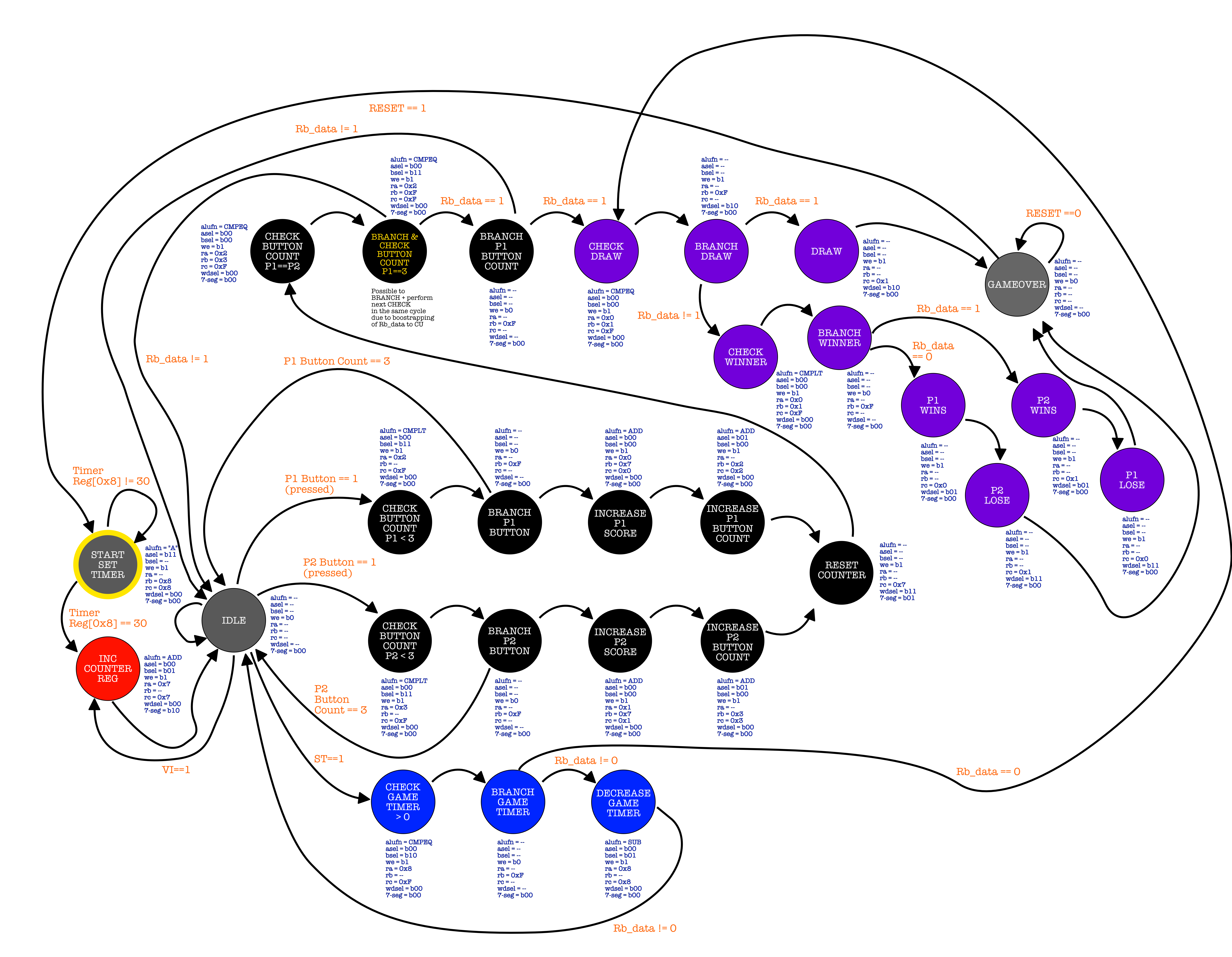
Button Press Event
BUTTON PRESS event is invoked when the control unit receives button press signal from either player.
When any player press a button, we want to check if the player’s current button press is less than 3.
- If yes, increment the button count, and increment the player’s score based on the current collectible number in the counter, and then reset the counter.
- If no, then no score update / counter reset is done.
We also have to check if both players have pressed their buttons for 3 times each as well. The game is supposed to end early if all players have used up their button presses regardless of time left.
- If yes, proceed to
COMPUTE WINNERevent. - Otherwise, go back to
IDLEstate.
Counter Increment Handling
INCREASE COUNTER event accounts for the fact that the control unit should receive some “random/varying” increment signal input from another unit. Whenever this variable increment machine produces a 1, then we need to handle this event by increasing the counter reg, and going back to the IDLE state.
The final output displayed to the user is as if the counter increases at unpredictable rate.
Timer Decrement Handling
DECREASE TIMER even accounts for the fact that the control unit should also receive some signal from a slow timer unit (that produces 1 every second instead) and decrement the timer register accordingly. A check on whether the timer register has reached zero has to be performed at the beginning of this event, and if so, proceed to COMPUTE WINNER event instead of decreasing the timer further.
Hopefully it is obvious by now that each state is logically equivalent to a single instruction in a regular program and an event is like a function which is a collection of repeatable instructions; comprised of many states. Within each state, you need to decide the value of the appropriate all control signals.
Example
Lets understand this notion with an example.
Look at CHECK BUTTON COUNT P1<3 state. It is triggered (from IDLE) if P1 Button is pressed, and output the following control signals:
alufn = CMPLTasel = b00bsel = b11we = b1ra = 0x2rb = --rc = 0xFwdsel = b007-seg = b00
The first bit is a command for the external 7-seg representing the counter on whether they should +1. The second bit is to reset the counter.
This means that in this state, we are comparing (CMPLT) the content of Reg[0x2] (P1 Button Count Reg), with the constant 3 that can be routed into the B port of the ALU when bsel = b11.
The output of the ALU is stored at the temp register Reg[0xF] since rc=0xF and we=1. We do not use the output from the Rb_data port of the regfile and therefore it doesn’t matter what value rb (read address of Rb_data) is.
In the next cycle, we will arrive at the state BRANCH P1 BUTTON which will look at the content of Reg[0xF] and decide whether to return to IDLE or update P2’s score.
The same logic applies for any other state.
fsm in Lucid
Programming an FSM in Lucid is very easy. You only need to import the fsm module and declare the states in the beginning. Then, in the always block things are repetitive: specify what output signals to be produced, and given input signals, specify the next state to go to. The code for the control unit can be found in here.
The Complete Datapath
The complete datapath for the sample Counter game should look like this. In fact, this basic structure can be adapted to implement any simple game.

The complete code that describes the datapath along with the connection to the control logic can be found here.
The black boxes signifies connection to external input/output devices. Interfacing with external devices is tricky, and may be frustrating at first. So it is important for you to finish ALL basic the other basic FPGA tutorials.
In particular, you need to know how to do smaller sub-components that are crucial to your project. For example, in this project you need to know how to:
- Debounce a button press, and only producing a value
1ONCE per button press using an edge detector. - Create a small combinational logic module to produce a value of
1ONCE every second (denoted asSLOW TIMER). You can use a basiccountermodule set withDIV:counter slow_timer(#SIZE(1),#DIV(26));- And use an edge detector
- Create a combinational logic module that randomly produce a value of
1(denoted asVARIABLE INCREMENTER). You can see the code here.
Notice the bootstrapped REGFILE output: all 16-bits Rb_data straight to the FSM. This is similar to the Z unit in \(\beta\) used for branching after a comparison check in the previous state. You can also use this to branch and perform next check in 1 cycle. The relevant state illustration and its sample lucid code is:

game_fsm.BRANCHCHECK_P1P2BUTTONCOUNT:

	regfile_read_address_b = b1111; //temp reg
	if(regfile_datain[0]){
		alufn = b110011; //CMPEQ
		regfile_read_address_a = b0010; //P1 button reg
		bsel = b11; //constant 3
		we_regfile = 1;
		regfile_write_address = b1111; //temp reg
		game_fsm.d = game_fsm.BRANCH_P1BUTTONCOUNT;
	}
	else{
		game_fsm.d = game_fsm.IDLE;
	}
Notice that the same game functionality can be implemented with less states if we merge all the branch + next check/computation states into a single state. As an example, we chose to display almost all branching state except the BRANCH CHECK BUTTON COUNT P=3 state above as purely a branching state without performing further computation – similar to how its done in \(\beta\).
Tips
If you are a beginner, then perhaps it is easier to debug if you simplify your states (even though you end up with more states).
Summary
It will help tremendously if you started by designing the blueprint of your game machine before you start coding. For Checkoff 2, you are required to present to us the:
- Game Idea
- Datapath
- State Transition Diagram
Prepare your complete datapath diagram and state transition diagram (handwritten is fine) as shown in the example above for your 1D Project Checkoff 2. You are highly recommended to keep your standard comparable, or better (by designing a proper instruction set, a RAM, and PC unit) than the example presented above.