 50.002 CS
50.002 Computation Structures
Information Systems Technology and Design
Singapore University of Technology and Design
Written by: Natalie Agus (2023)
Lab 4: Beta Processor with FPGA (Part 2)
In this second part of the lab, we will learn about further implementations to operate our Beta CPU:
- To run a tester code that demonstrate basic instructions:
OP/OPC, control transfer (BNE/BEQ/JMP), and memory access (LD/ST) with a slowclock, faster clock, and manually - To view the system’s states (e.g:
ma,ia,id, etc) at the 7-seg as part of debug protocol - To view the system’s output buffer at the 7-segment
- To interact with the system (triggers hardware interrupt
irq, handle I/O) - To trigger
ILLOP(software interrupt) and demonstrate how it is handled
You are not required to submit your code for this lab. Simply head to eDimension and do the lab questionnaire by the stipulated due date. Please also complete the Checkoff to this lab, which is to demonstrate that the simple tester source code from the previous week works as intended following the screenshots provided in the previous lab. You shall do your checkoff as a group. Only group members who are present gain the marks (unless valid LOA).
Beta Tester Source Code
We have written a simple 28-line tester code for your Beta inside instruction_rom.luc. Unfortunately, we don’t have a nice auto-tester and auto-graded checkoff file like we have in jsim. We just need to either manually ensure that the outputs are correct by observing each state of the Beta (PC content, Regfile content, control signals, etc) at each instruction execution or write an automatic tester like you did for your ALU in Checkoff 1.
The instruction is as follows. Notice that the first instruction (address 0) is placed at the bottom of the arrow to follow Verilog/Lucid array convention.
   // Driver code, BR(reset) is the first instruction
  const INSTRUCTIONS = {
    32h6FE50000, // 0x06C JMP(R5)
    32hC0BF000C, // 0x068 ADDC(R31, 12, R5) --- reset handler, go to main in user mode
    32h6FE50000, // 0x064 JMP(R5)
    32hC0BF000C, // 0x060 ADDC(R31, 12, R5)
    32h649F000C, // 0x05C ST(R4, 0xC, R31)
    32hC09F0001, // 0x058 ADDC(R31, 1, R4)
    32h649F000C, // 0x054 ST(R4, 0xC, R31)
    32hC09F0002, // 0x050 ADDC(R31, 2, R4)
    32h649F000C, // 0x04C ST(R4, 0xC, R31)
    32hC09F0003, // 0x048 ADDC(R31, 3, R4)
    32h649F000C, // 0x044 ST(R4, 0xC, R31)
    32hC09F0004, // 0x040 ADDC(R31, 4, R4)
    32h649F000C, // 0x03C ST(R4, 0xC, R31) --- countdown 5, 4, 3, 2, 1 to be be displayed at beta_output
    32hC09F0005, // 0x038 ADDC(R31, 5, R4) --- illop handler, show generic countdown
    32h6FE50000, // 0x034 JMP(R5) --- execute main
    32hC0BF000C, // 0x030 ADDC(R31, 12, R5)
    32h649F000C, // 0x02C ST(R4, 0xC, R31) --- store to output_buffer: Mem[12] to display the input
    32h609F0010, // 0x028 LD(R31, 16, R4) --- irq handler, load value from input_buffer: Mem[16]
    32h00000100, // 0x024 LONG(256) --- trigger illop when R3's value is eventually 0 after several loops to main_sub
    32h7BE3FFFB, // 0x020 BNE(R3, main_sub, R31)
    32h607F0020, // 0x01C LD(R31, 32, R3)
    32h643F0020, // 0x018 ST(R1, 32, R31)
    32h90410800, // 0x014 CMPEQ(R1, R1, R2)
    32hC4210001, // 0x010 SUBC(R1, 1, R1) --- main_sub
    32hC03F0003, // 0x00C ADDC(R31, 3, R1) --- main
    32h77FF0007, // 0x008 BR(irq)
    32h77FF000C, // 0x004 BR(illop)
    32h77FF0019  // 0x000 BR(reset)
  };
Here’s the equivalent instruction that can be run on bsim:
.include beta.uasm

|| This code will not work as-is in bsim because in beta lucid we separate data memory and instruction memory
|| Edit the value of message and test_value below to run it in bsim

message = 0xC || replace to 0xCC for bsim, 0xC for lucid
test_value = 32 || replace to 128 for bsim, 32 for lucid

BEQ(R31, reset, R31) 	|| reset handler  0x00000000
BEQ(R31, illop, R31) 	|| illop handler  0x00000004
BEQ(R31, irq, R31)  	|| irq handler    0x00000008

||| USER PROGRAM |||
main: ADDC(R31, 3, R1)	|| main program
main_sub: SUBC(R1, 1, R1)
CMPEQ(R1, R1, R2)
ST(R1, test_value)
LD(R31, test_value, R3)
BNE(R3, main_sub, R31)
LONG(256) 		|| test trigger illop after 3 loops of main_sub
||||||||||||||||||||

|| IRQ HANDLER, KERNEL PROGRAM ||
irq: LD(R31, 16, R4)	|| load hardwired value at input_buffer (Mem[16])
ST(R4, message, R31)	|| store (display) input value at output_buffer (Mem[12])
ADDC(R31, 12, R5)
JMP(R5)			|| jump to execute main program in user mode
|||||||||||||||||||||||||||||||||

|| ILLOP HANDLER, KERNEL PROGRAM ||
illop: ADDC(R31, 5, R4)	|| countdown: 5,4,3,2,1 to mimmick illop handling
ST(R4, message, R31)
ADDC(R31, 4, R4)
ST(R4, message, R31)
ADDC(R31, 3, R4)
ST(R4, message, R31)
ADDC(R31, 2, R4)
ST(R4, message, R31)
ADDC(R31, 1, R4)
ST(R4, message, R31)
ADDC(R31, 12, R5)
JMP(R5)			|| jump to execute main program in user mode
|||||||||||||||||||||||||||||||||||

|| RESET HANDLER, KERNEL PROGRAM ||
reset: ADDC(R31, 12, R5)
JMP(R5)			|| jump to execute main program in user mode
|||||||||||||||||||||||||||||||||||
We do not actually instantiate a memory unit with 32-bit addressing. Hence we do not physically separate Kernel program vs User program for this lab (demonstration purposes only). In reality, kernel program resides in the memory region with address MSB of 1, and user program resides in the memory region with address MSB of 0. To prevent User Program main from executing the irq handler that’s placed right after it, we design the main to end with a constant LONG(256) which will officially trigger an ILLOP situation.
Operating the Beta
It should be fairly easy for you to know what the tester program do. We have three handlers in address 0, 4, and 8 respectively to handle what has to be done in the event of reset, illop, and irq. The actual implementation of the handlers reside in label reset, illo, and irq respectively.
- When you have implemented the
beta_cpusuccesfully and compiled it, ensure that ALL switches are down. - Load the compiled binary to the FPGA. At this point, your PC is pointing to
Mem[0x0]. Useio_dup[0]to inspect the states of the Beta CPU. - Press the
nextbutton:io_button[4](right button) to execute the next instruction. - Refer to
README.mdinside the repository for more information on how to operate the Beta CPU automatically.
Debug Signals
As a reminder, io_dip[0] can be changed to “view” various states presented at io_led[1] and io_led[0] (16 bits of values at once). Simply set it to represent the values below, e.g: 0x3 means that io_dip[0] is set to 00000011 (turn the rightmost two switches on). Here are the exhaustive list:
0x0: MSB 16 bits of current instruction (id[31:16])0x1: LSB 16 bits of current instruction (id[15:0])0x2: LSB 16 bits of instruction address (ia[15:0])0x3: LSB 16 bits of EA (this is also ALU output) (ma[15:0])0x4: MSB 16 bits of EA (this is also ALU output) (ma[31:16])0x5: LSB 16 bits of Mem[EA] (mrd[15:0])0x6: MSB 16 bits of Mem[EA] (mrd[31:16])0x7: LSB 16 bits of RD2 (mwd[15:0])0x8: MSB 16 bits of RD2 (mwd[31:16])0x9: LSB 16 bits of pcsel_out0xA: LSB 16 bits of asel_out0xB: LSB 16 bits of bsel_out0xC: LSB 16 bits of wdsel_out0xD: MSB 16 bits of instruction address. Useful to see PC31 (kernel/user mode) (ia[31:16])0xE: LSB 16 bits of beta input buffer. This is a dff that’s hardwired to reflect Mem[0x10]0xF: LSB 16 bits of beta output buffer. This is a dff that’s hardwired to reflect Mem[0xC]
We have also provided all this information in the repository’s readme.
The slowclk
The entire system runs on FPGA clk. However we need some other signal to slow down specifically the Beta CPU PC advancement so that we can observe the CPU’s states like id,ia, ma, mrd, mwd, output of all muxes (pcsel mux, asel mux, bsel mux, and wdsel mux), as well as the value of I/O buffers. As such, we need additional logics to prevent the PC from advancing too fast.
The Beta expects an input called slowclk so that you can slowly observe its execution (either by pressing io_button[4] or when slowclock_edge or fastclock_edge fires). The slowclock_edge turns 1 roughly once (for a single FPGA clock cycle) every 1.3s, and fastclock_edge is roughly 4 times faster than slowclock_edge. You can use io_dip[2][6] to enable/disable fastclock.
It is necessary for slowclock and/or fastclock period to be at least 5 times longer than Alchitry Au FPGA’s because of how fsm motherboard is designed in au_top.luc (see next section). That is, the minimum index of frequency_divider in au_top.luc that can be used for slowclock and/or fastclock is 2 (index 0 is LSB).
Right now in au_top.luc, we are using index 27 and 25 so that you have sufficient time to observe its output:
    // driving the beta
    slowclock_edge.in = frequency_divider.value[27];
    fastclock_edge.in = frequency_divider.value[25];
User I/O
The system is designed to have the following input and output unit for user interaction:
- Input:
io_button[2:0]triggers interrupt (hardwired). This is the up, middle, and down button. - Output: set
io_dip[0]to:00001111(0x0F) and the output will be displayed at the 7seg. This is your “screen”.
When io_button[0], io_button[1], or io_button[2] is pressed, we write some logic in au_top.luc to store its encoding to system_input_buffer and system_output_buffer (32 bit dff) defined in motherboard.luc.
    // in au_top.luc

    // connect hardware interrupt button
    interrupt_button_conditioner.in = io_button[2:0];
    interrupt_button_edge.in = interrupt_button_conditioner.out;
    motherboard.irq = interrupt_button_edge.out; // IRQ as long as any of of the buttons[2:0] is pressed

    ...

    // display the content of output_buffer
    h0F: // LSB 16 bits of system_output_buffer
      io_led[1:0] = {motherboard.output_buffer[15:8], motherboard.output_buffer[7:0]};
      seg.values = {motherboard.output_buffer[15:12], motherboard.output_buffer[11:8], motherboard.output_buffer[7:4],motherboard.output_buffer[3:0]};
    // in motherboard.luc

    // store the button press to input buffer
    if (|irq){
      if (irq[0]){
            system_input_buffer.d = 32hB0;
      }
      else if (irq[1]){
            system_input_buffer.d = 32hB1;
      }
      else if (irq[2]){
            system_input_buffer.d = 32hB2;
      }
    }
These buffers are then synchronized to a specific region in memory_unit so that your Beta CPU can access its values.
The Motherboard
In practice, a motherboard is the main printed circuit board in general-purpose computers. It holds and allows communication between many of the crucial components of a system: the CPU, the memory unit, and provides connectors for peripheral (I/O) devices.
The module motherboard.luc is where we instantiate our major hardware components:
- The Beta CPU
- The memory unit (both data and instruction)
- System input and output buffer (
32bits each). This serves as a buffer that holds current input or current output value. The motherboard is connected to actual buttons (input) and LEDs (output) inau_top.luc. - The instruction ROM (for initial loading of instruction)
We define their connections and added a simple fsm motherboard that runs the Beta and handle I/O.
LOAD
Upon start up, LOAD instructions from instruction rom to the instruction memory part of the memory unit. We do not use the ROM directly to simulate a more realistic approach whereby upon boot up, we will load our data from disk (signified by this ROM) to our physical memory.
RUN
Once all instructions are loaded, we go to the RUN state. In the RUN state, we mostly “idle” and wait for the next slowclk to fire (advance the PC). When slowclk == 1, we need to deliberately do two things: refresh output and input buffers.
LOAD_OUTPUT and DISPLAY_OUTPUT
Firstly, to refresh our system_output_buffer. This is done by two states: LOAD_OUTPUT and DISPLAY_OUTPUT because our simple_dual_ram requires 1 FPGA clock cycle to be able to display the requested data at a given read address.
UPDATE_INPUT
Secondly, to refresh Mem[0x10] (so that it matches the content of system_input_buffer). This is done by a single state: UPDATE_INPUT. Afterwards, the motherboard goes back to the RUN state, until slowclk turns 1 again and the whole output and input update is done.
slowclk period
The content at Mem[0x10] will only reflect system_input_buffer until after we exit UPDATE_INPUT and enters the RUN state again. The soonest any other component can read the updated Mem[0x10] is two clock cycles from UPDATE_INPUT (UPDATE_INPUT –> RUN –> RUN). Hence if the current instruction involves LD from Mem[0x10], we need to make sure at least two RUN states happen after we exit from UPDATE_INPUT before slowclk fires. We also need at least three FPGA clk cycles have passed to account for RUN –> LOAD_OUTPUT –> DISPLAY_OUTPUT –> UPDATE_INPUT. In total, slowclk period must be at least five times longer than the FPGA clk period.
Storing to REGFILE
While waiting for the slowclk, our Beta has received id and mrd (whenever applicable). It is also continuously supplying all output to the memory_unit: ia, wr, ma, and mwd. In other words, it continuously execute the same instruction over and over for the duration of the period of slowclk. To avoid having repercussions we need to take care of the werf signal in the regfile_unit.
It should NOT continuously write to regfile_unit. Notice this line in regfile_unit.luc:
    // do not write anything to the regfile unless PC advances
    regfile.write_enable = 0;
    if (slowclk) {
      regfile.write_enable = werf;
    }
The purpose of this line is to avoid instructions that read from and write to the same register e.g: ADDC(R0, 1, R0) to not be executed many times for the duration of the slowclock period. Remember that all our sequential logic devices still run on clk, which is the actual FPGA clock signal. We simply add additional logic in the pc_unit.luc so that we advance our instruction when slowclk fires. Suppose for each period of slowclk, 200 FPGA clk cycles has passed. If we do not set regfile.write_enable = 0, we are effectivelly running the instruction ADDC(R0, 1, R0) for 200 times (instead of once!) and we will have the value 200 inside R0 instead of 1 as per the instruction.
Warning
For most instruction, it is okay to repeatedly execute that instruction many times, once per
clkcycle while waiting for the nextslowclkrising edge so at first blush it seems hard to come up with the conclusion thatregfile.write_enablemust be set to 1 for just exactly oneclkcycle and0otherwise.For instance,
ADD(R1, R2, R3)will repeatedly write the content ofR1+R2and store it at R3, andST(R5, destination, R31)will repeatedly store the content ofR5toMem[destination]. The value inR3for theADDinstruction will remain the same even though we execute this instruction many times. The same works for theSTinstruction.However, if we read-and-modify the same memory region in the same clock cycle as we do with the Regfile:
ADD(R0, R0, R0), orMULC(R0, 3, R0), then we need to strictly run this instruction exactly once. Notice that only arithmeticOPandOPCwill suffer from this bug. This bug is not possible inST/LD/LDRbecause we can’tSTto andLDfrom the same memory region in the same cycle.
Finally, when slowclk turns 1 (rising edge), PC is set to advance in the next FPGA clock cycle. In this current cycle (the clk cycle when slowclk just had its rising edge), we are still executing the current instruction. This is when we capture the computed arithmetic output from the current instruction into the REGFILE.
Memory-Mapped I/O
We use Memory-Mapped I/O design to access input/output values as opposed to Isolated-Mapped (also known as port-mapped) IO.
As a result, we need to systematically update some region of the memory_unit to reflect the contents of system_input_buffer, and update system_output_buffer to reflect the content of a certain memory region in the memory_unit.
We choose memory_unit address 0x10 as the region to hold the last-received input value, and we choose memory_unit address 0xC as the region to hold the current output value.
That is if we were to STORE any value to Mem[0xC], it will reflected at the “output” of the motherboard. In practice, this will be the buffer containing values to be displayed at your screen. Similarly, if any input button io_button[2:0] is pressed, it will trigger an INTERRUPT, and you can find the encoding of the currently pressed button in Mem[0x10]. This will be the buffer containing the currently received input (e.g: keyboard keypress).
Sample Run
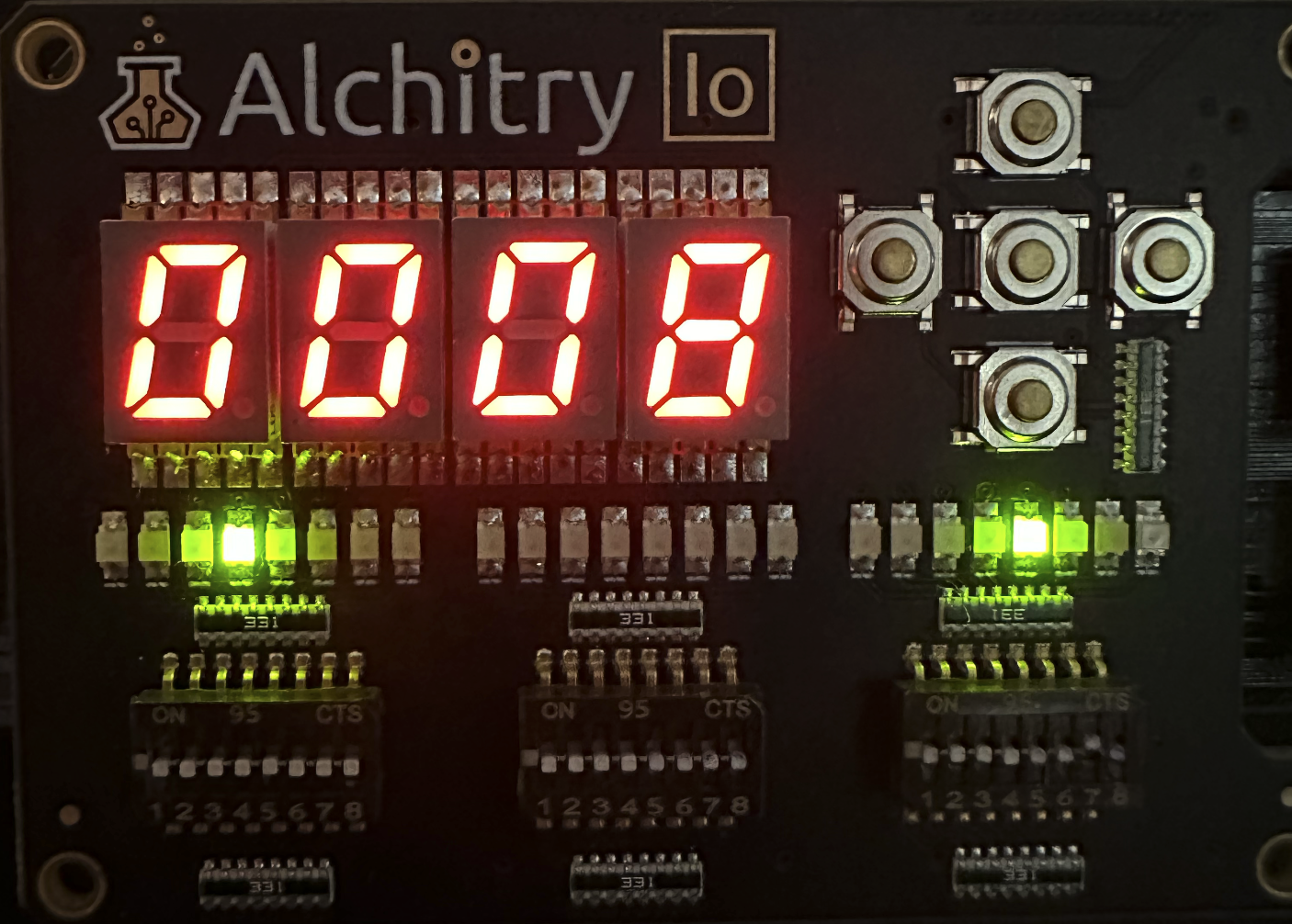
This section illustrates what should be observed on your FPGA IO Shield. When you compile the program above and flash it to your FPGA for the first time with all of its dip switches down, you will see the following as the first 16 bit of your instruction:
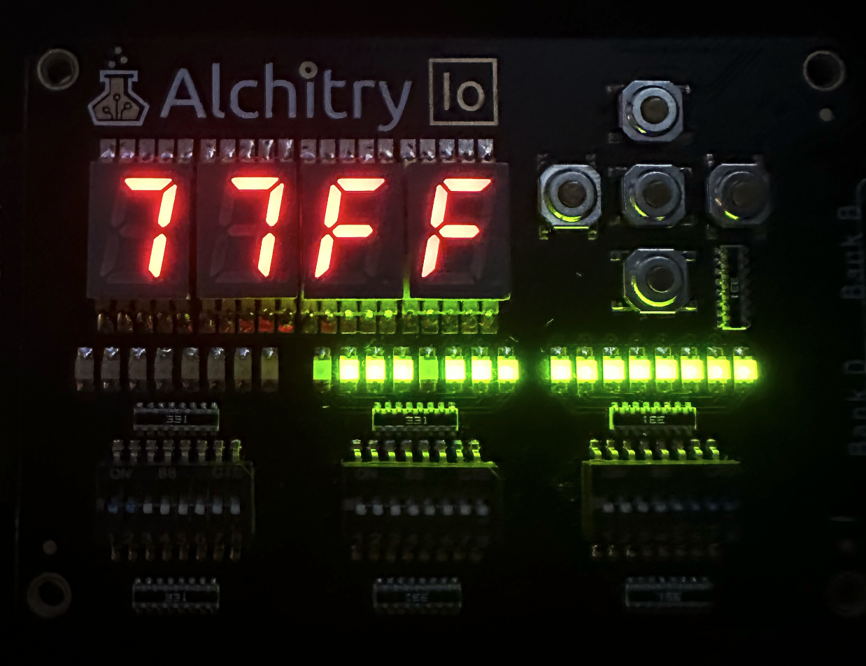
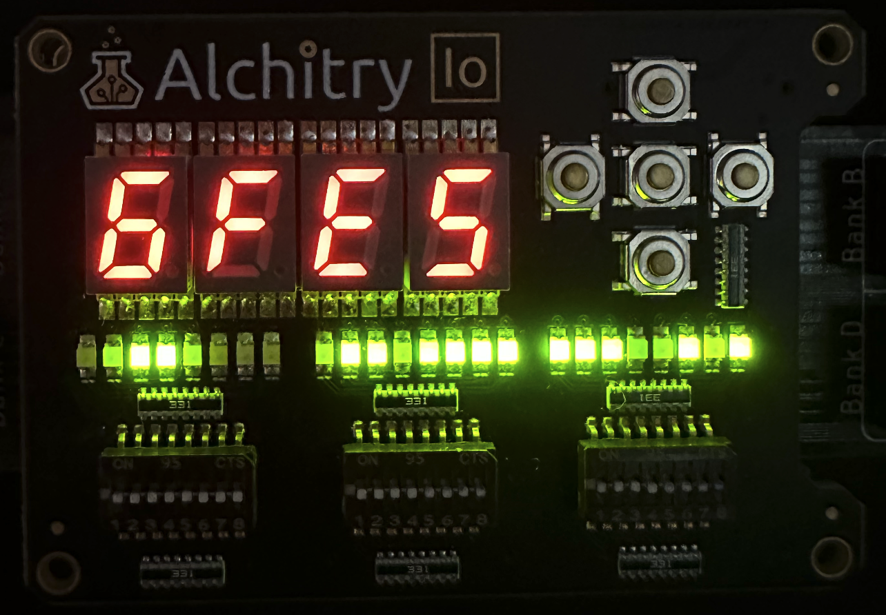
This corresponds to BR(reset): 0x77FF0019. Pressing the next button (io_button[4]) will bring you to address 0x068 which is the reset handler, having the same MSB 16 bit of the id: 0x77FF.
We assume you know which dip switch to set to view these states: ia, id, etc.
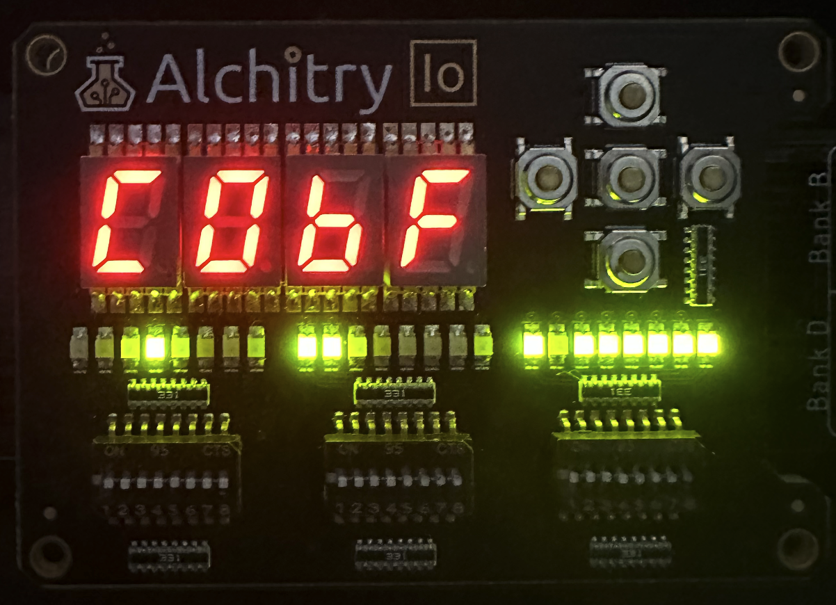
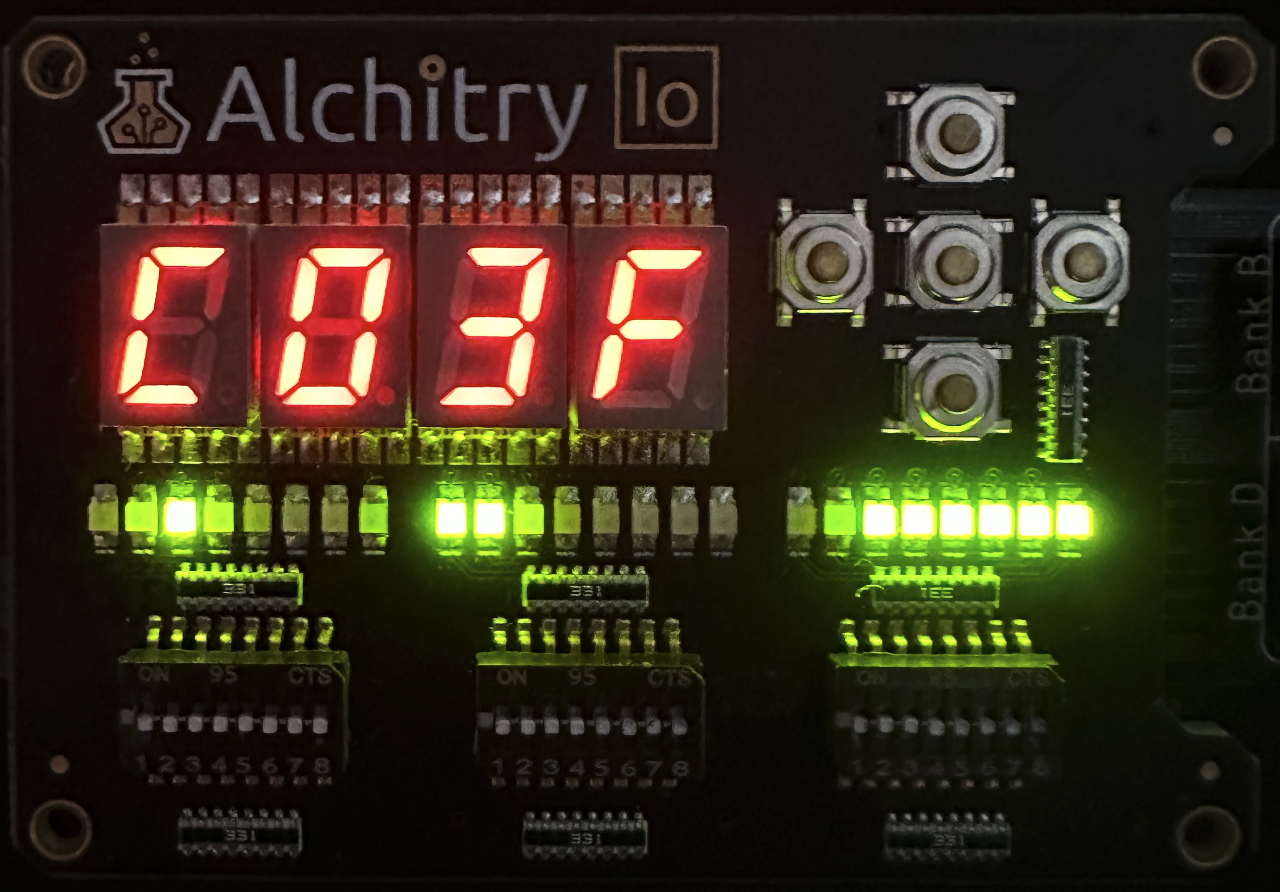
The first line of instruction in the reset handler is ADDC(R31, 12, R5): 0xC0BF000C:
Press next one more time and confirm you’re met with the JMP(R5) instruction (the MSB 16):
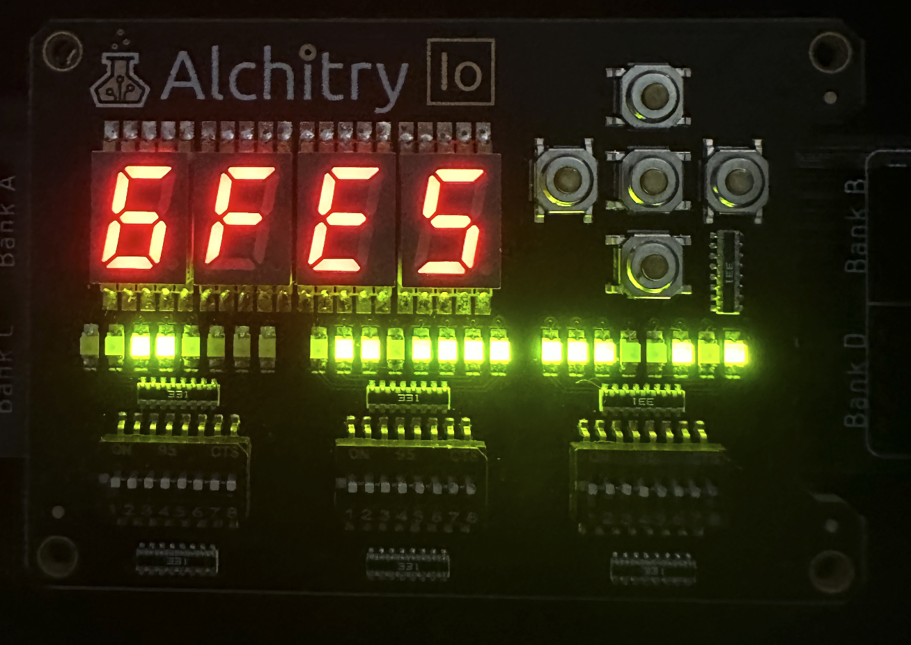
At this point, the content of Reg[R5] is address 0x00C. Pressing next will bring your PC to point to this address with instruction ADDC(R31, 3, R1): 0xC03F0003.
Continuously press next until you reach address 0x020, the BNE(R3, main_sub, R31) instruction:
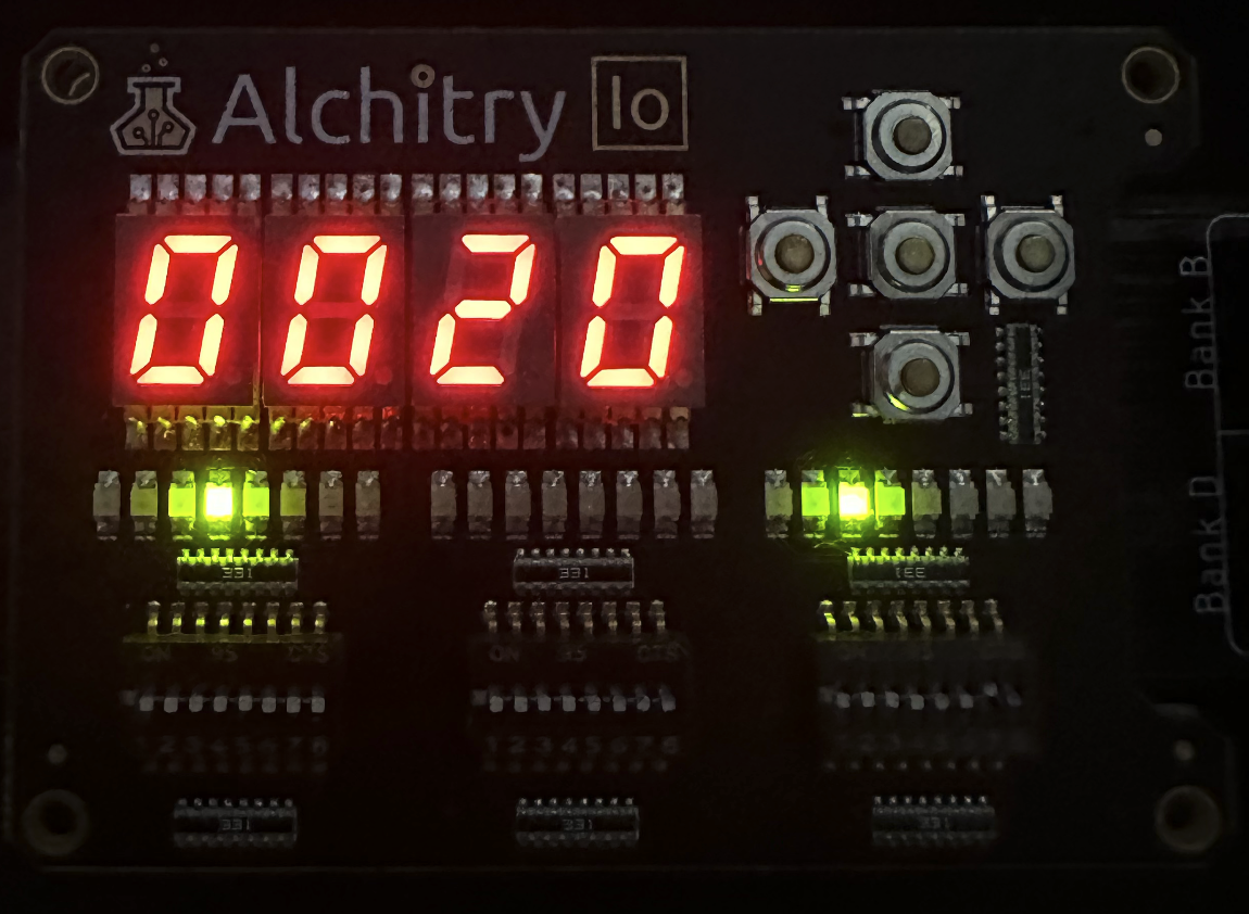
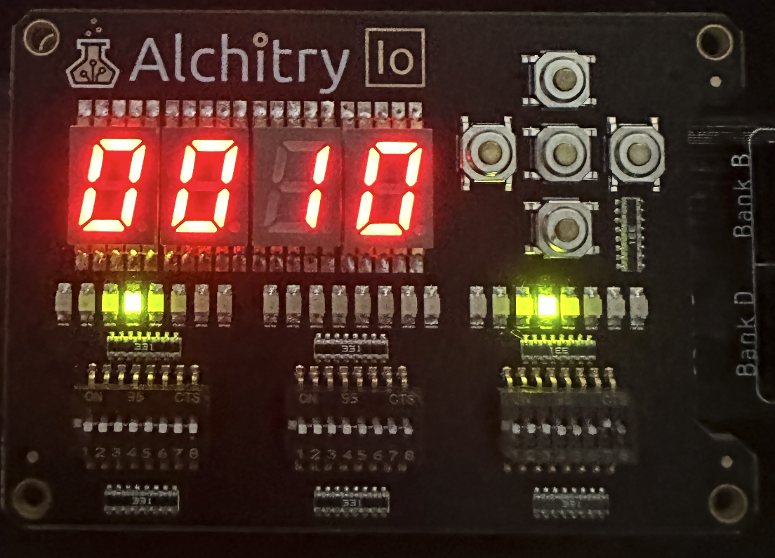
At this point, the content of R3 is 2, which means that you will be looped back to main_sub (adress 0x010). Press next to confirm the content of PC is indeed 0x010:
Triggering ILLOP
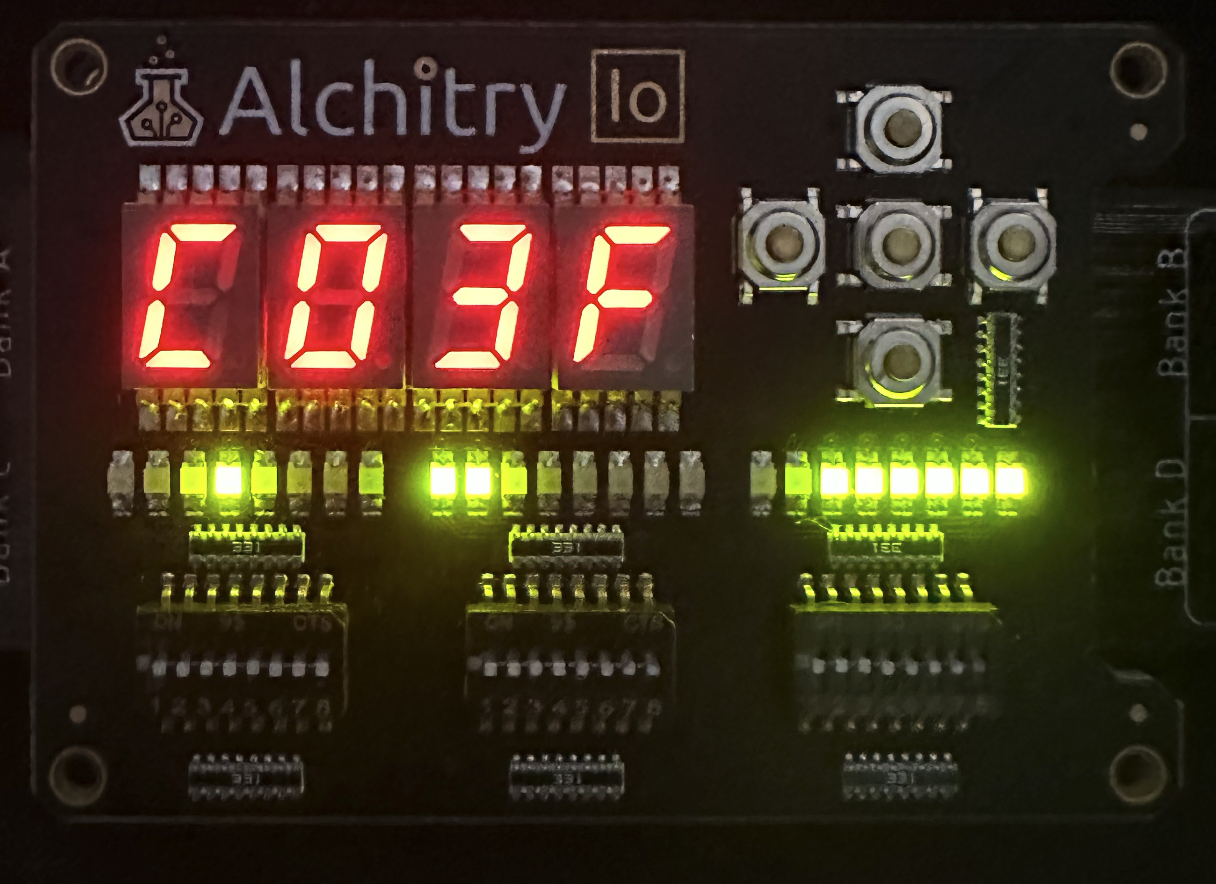
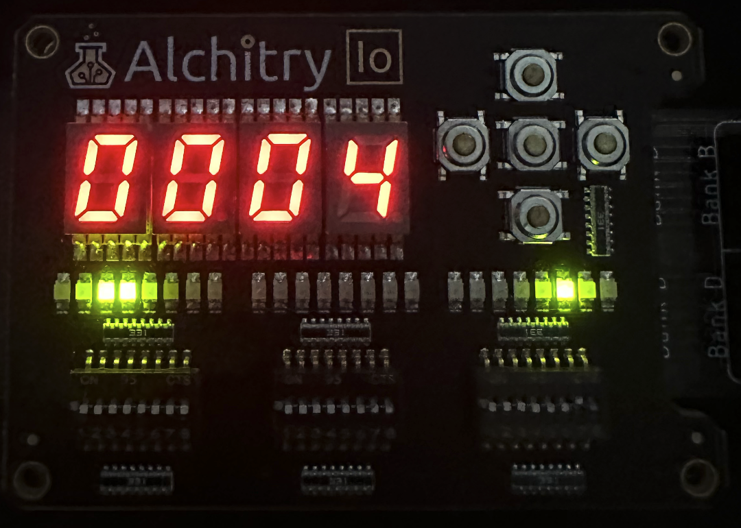
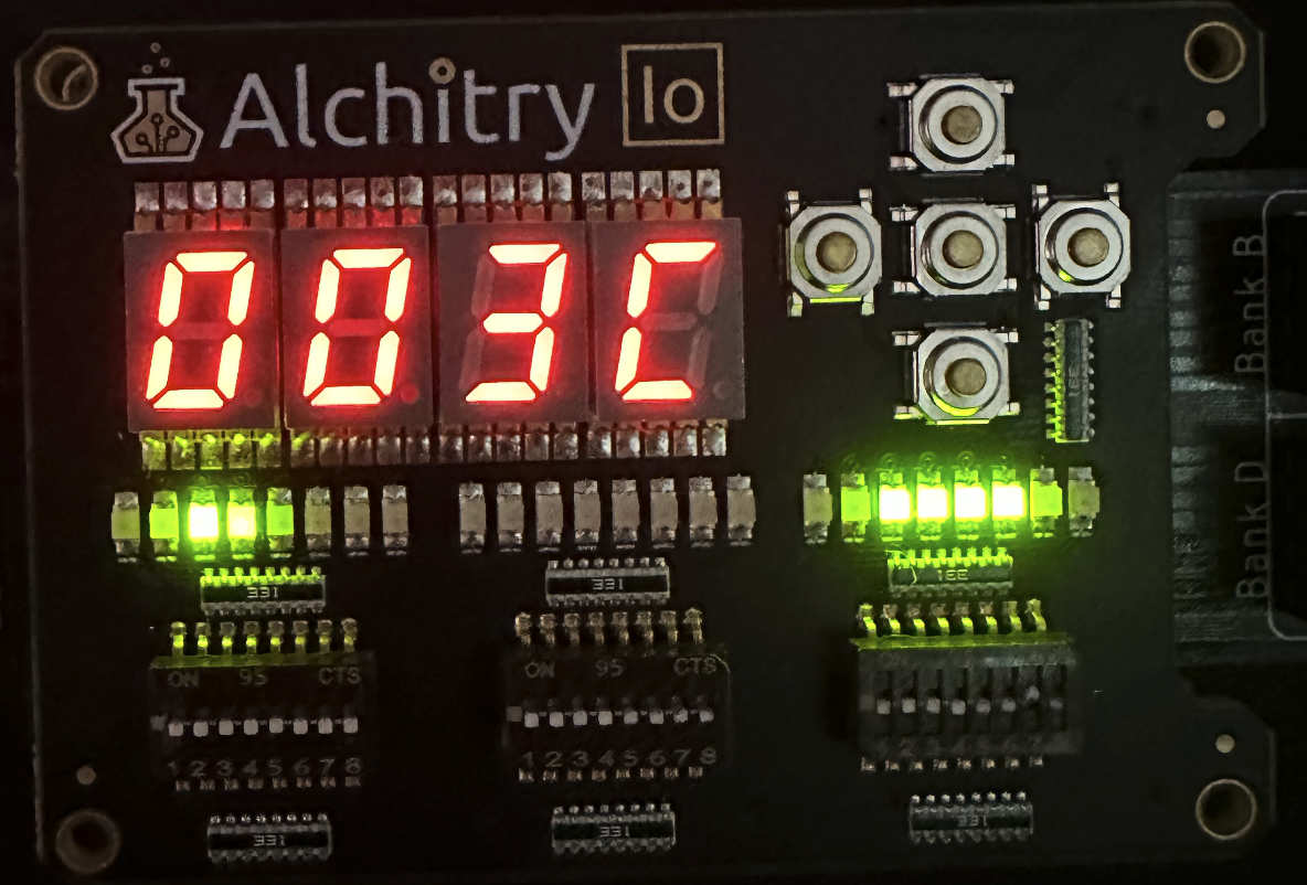
The content of R3 will be reduced by 1 in each loop to main_sub, until eventually its content is 0. This will cause BNE(R3, main_sub, R31) to not branch, and the PC will execute instruction at address 0x024 instead:
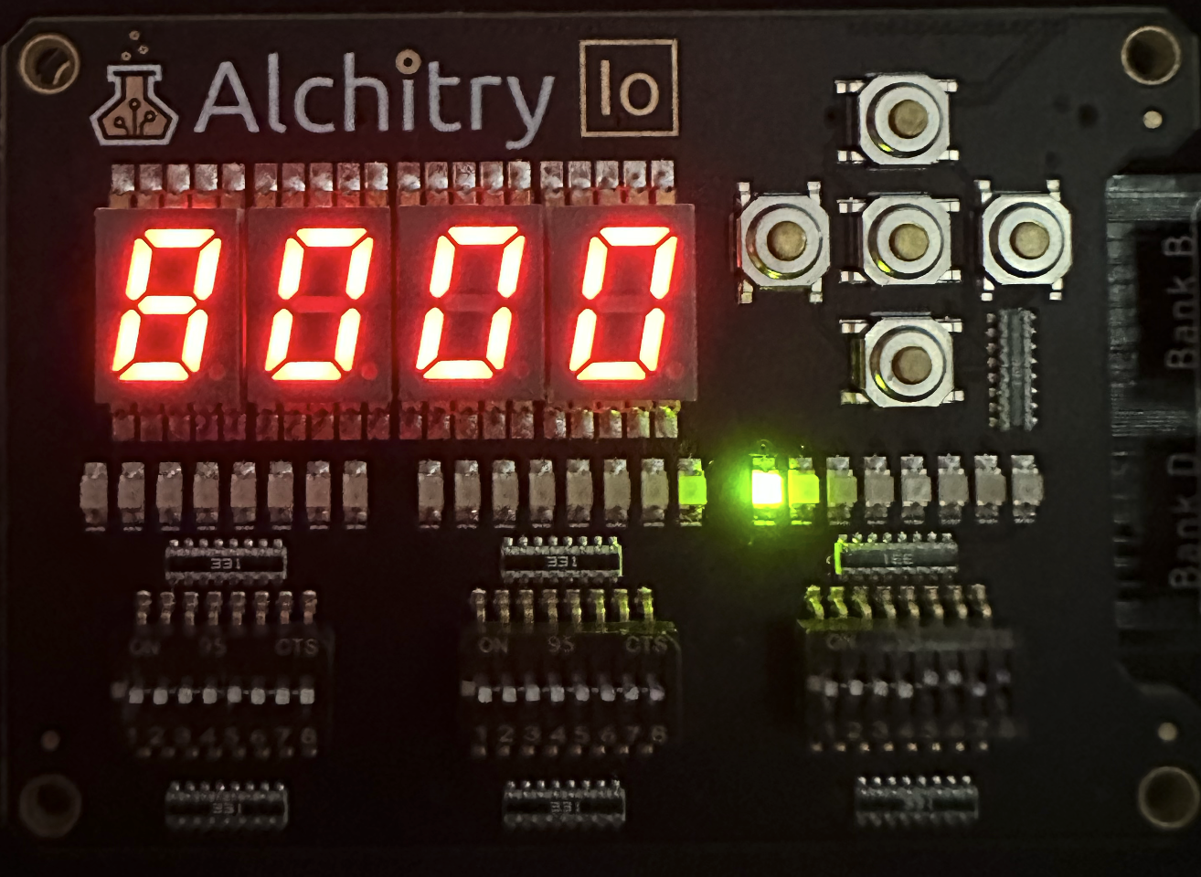
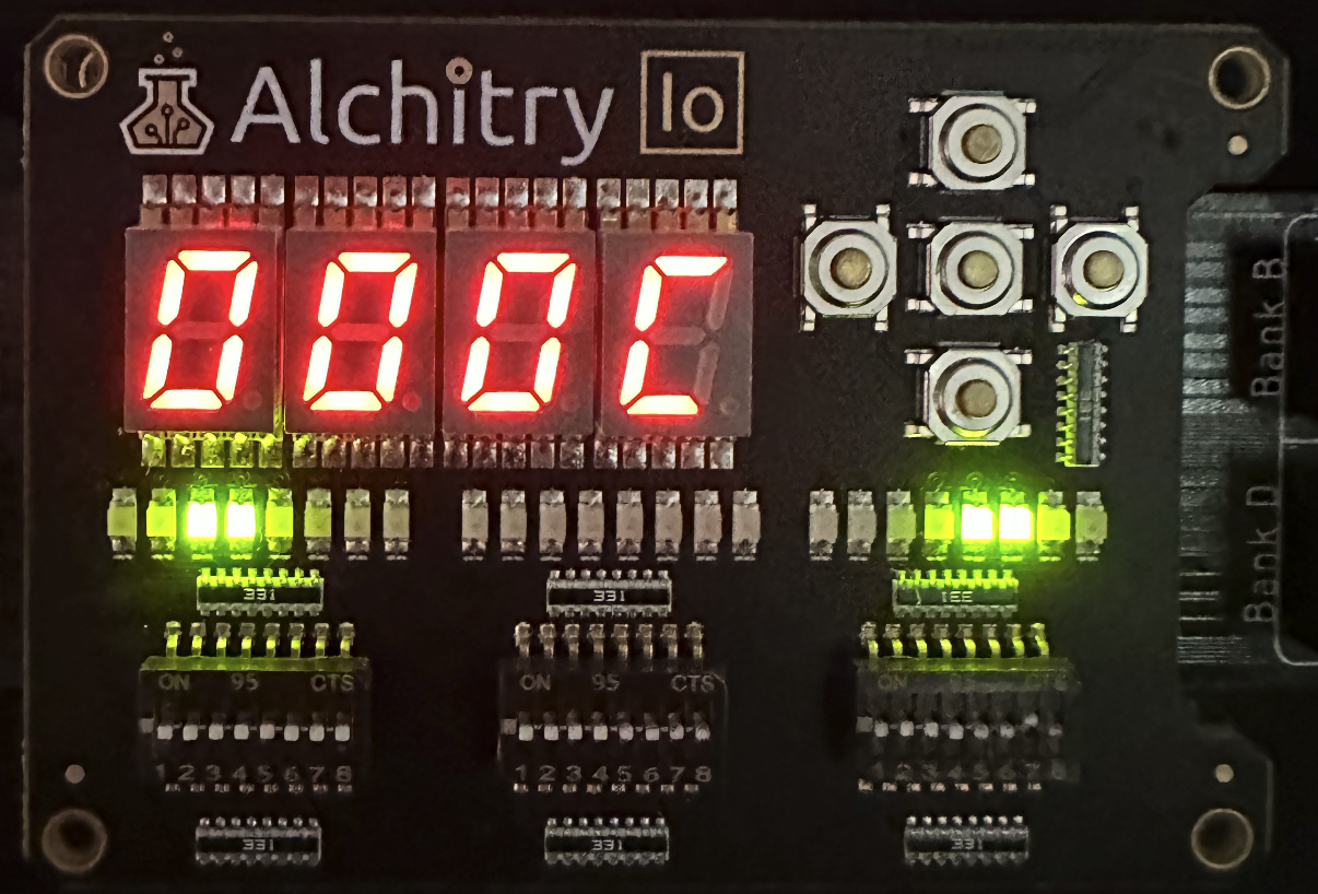
The instruction at address 0x024 is LONG(256), which is not a valid Beta instruction. Executing this will trigger an ILLOP. When you press next, you will be brought to address 0x004 which contains instruction BR(illop).
Note that at this point, the MSB of the PC (we also call this PC31) is 1, which means that the CPU is supposedly at the kernel mode. This is also known as the supervisor bit
You can set io_dip[0]: 0xD to confirm:
The ILLOP handler
The illop_handler resides at address 0x80000038 to address 0x8000064, but for the ease of explanation, we simply report the last 3 hex digits. Surely enough when you press next, the PC will point to address 0x038, which is the beginning of the illop_handler:
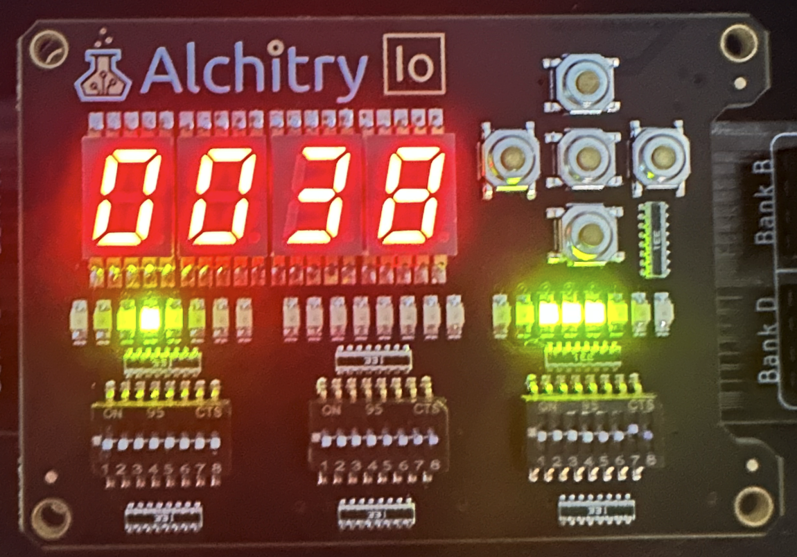
The ILLOP handler does a very simple thing, which is simply storing the value 5, 4, 3, 2, 1 to a particular memory address message.
message is set to be 0xC in our FPGA, which is a memory-mapped region to showcase our “output” to the system_output_buffer.
|| ILLOP HANDLER, KERNEL PROGRAM ||
illop: ADDC(R31, 5, R4)	|| countdown: 5,4,3,2,1 to mimmick illop handling
ST(R4, message, R31)
ADDC(R31, 4, R4)
ST(R4, message, R31)
ADDC(R31, 3, R4)
ST(R4, message, R31)
ADDC(R31, 2, R4)
ST(R4, message, R31)
ADDC(R31, 1, R4)
ST(R4, message, R31)
ADDC(R31, 12, R5)
JMP(R5)			|| jump to execute main program in user mode
|||||||||||||||||||||||||||||||||||
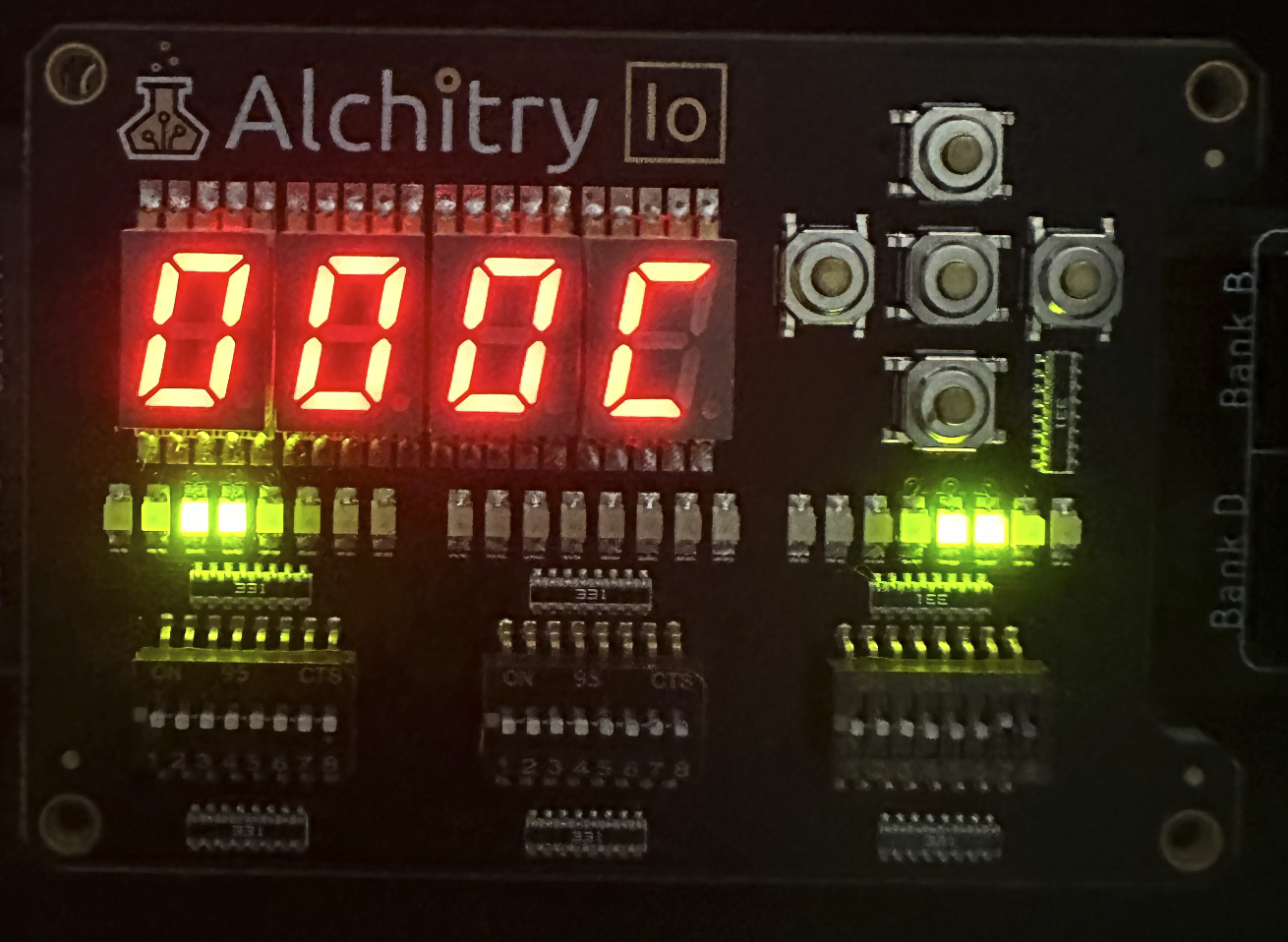
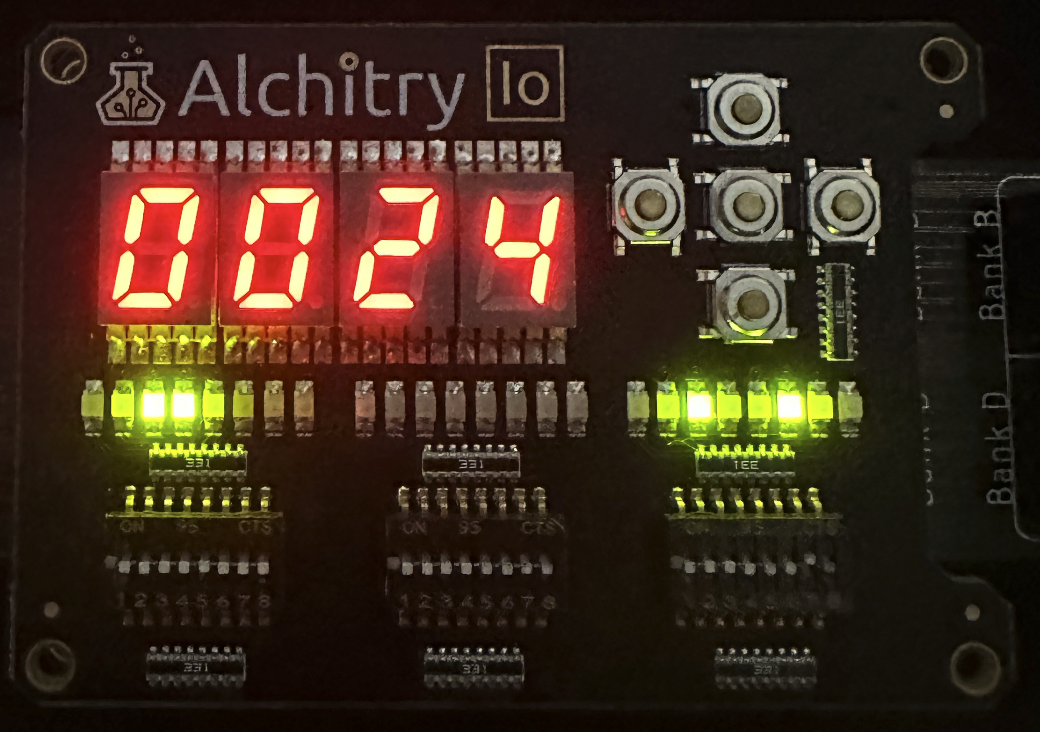
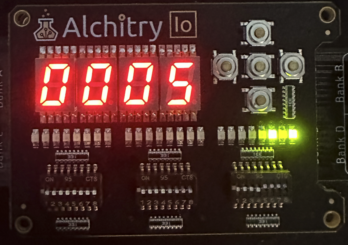
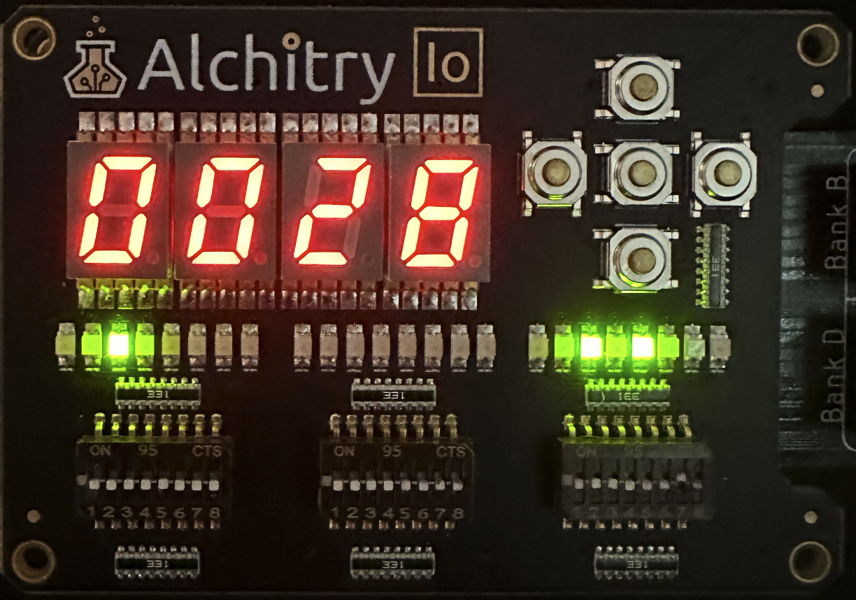
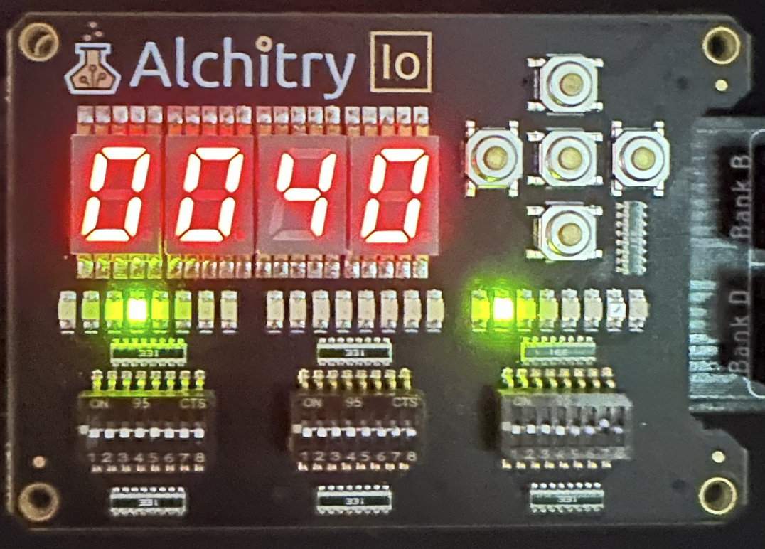
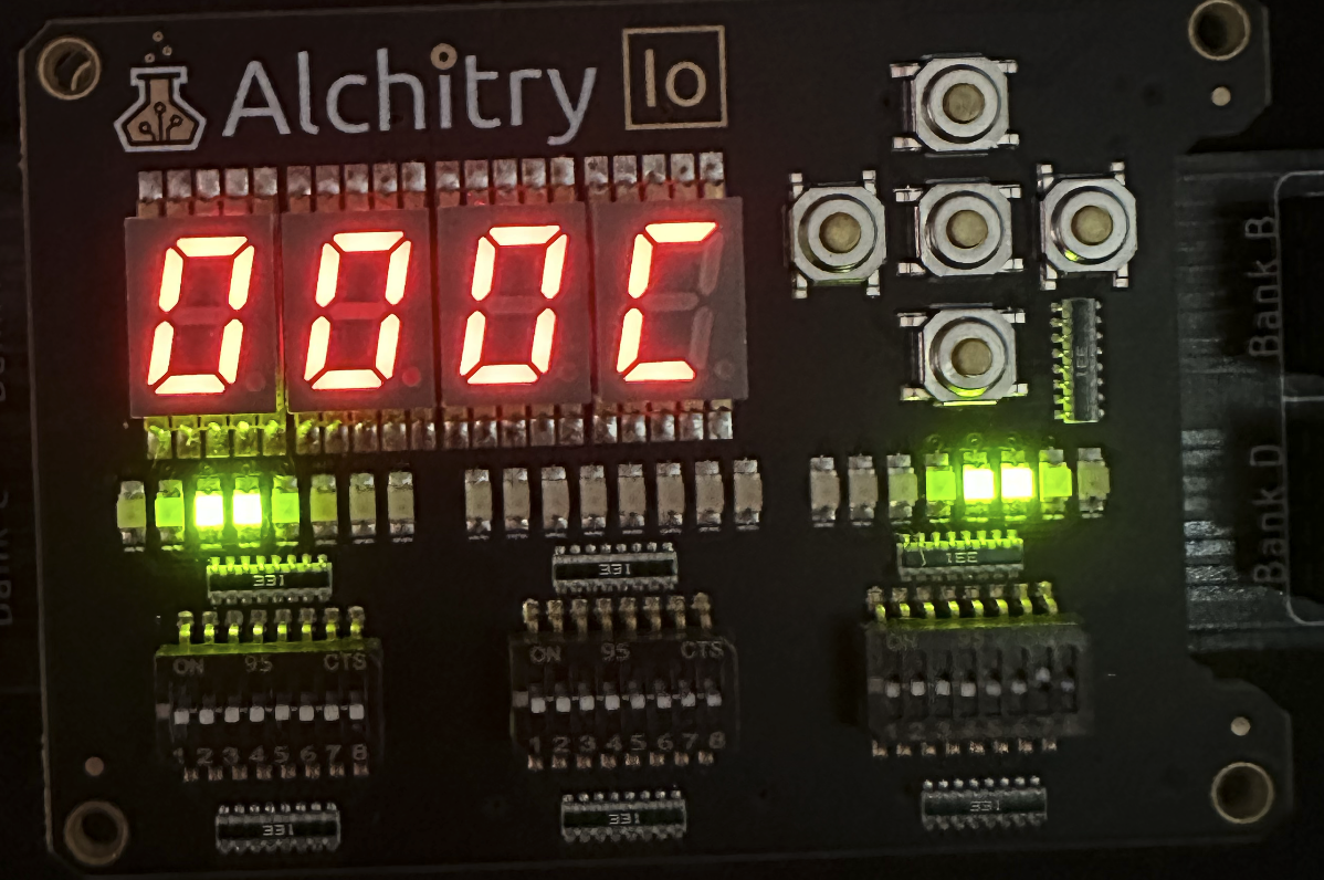
Advance to address 0x040.
<img src=”/50002//assets/images/lab4-part2/2023-03-16-17-57-00.png” class=”center_fifty no-invert/>
Then set io_dip[0] = 0xF to view the content of system_output_buffer. You shall see the value 5 there.
To witness it going from 5 to 4, 3, 2, 1, simply switch up io_dip[2][7]. This triggers the auto execution mode with the slow clock. If you are impatient, you can switch up io_dip[2][6] as well and it will advance the PC at a faster rate.
Returning to main (user mode program)
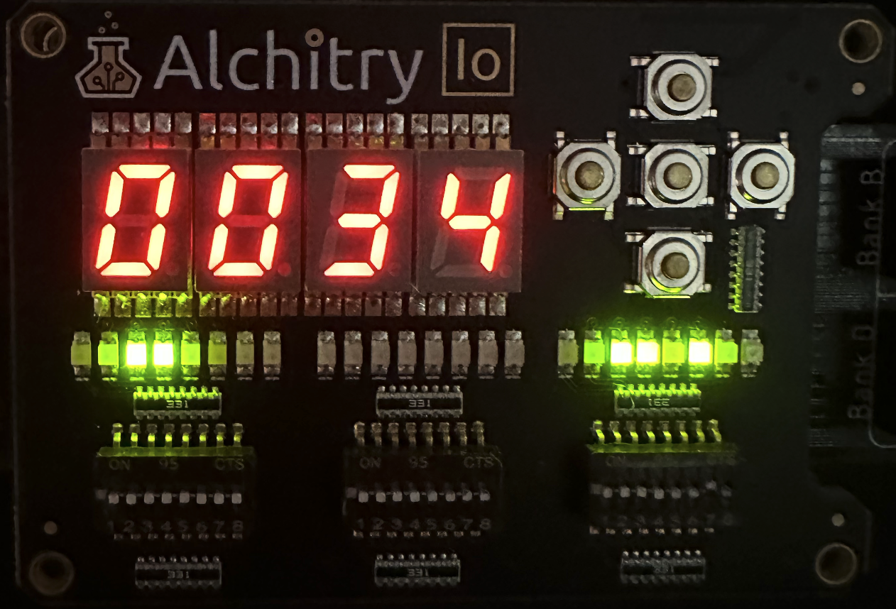
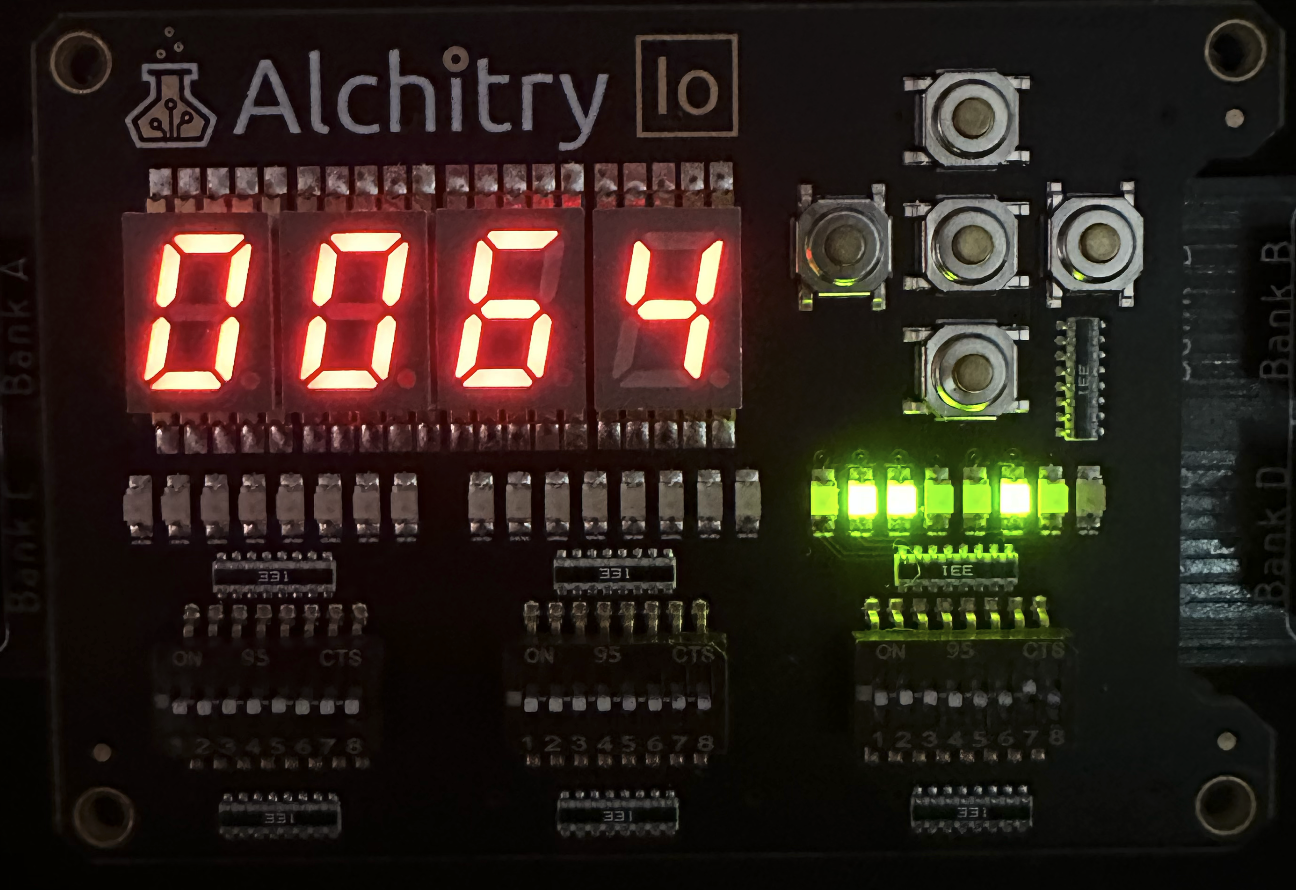
Once we reach address 0x064, we are met with the instruction JMP(R5).
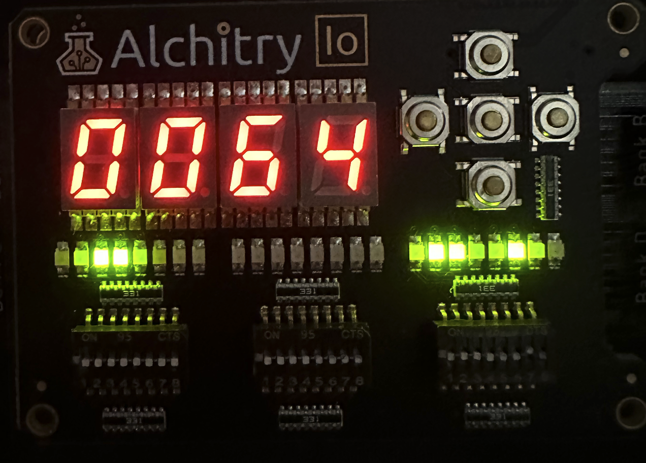
At this point, the content of R5 is 12 or 0xC, which means that it should execute address 0xC later in user mode. If you press next, you will meet the instruction ADDC(R31, 3, R1) again (main):
Surely enough, we are back at user mode. You can confirm this by inspecting the MSB of the PC:
Receive user input
You can press any button: io_button[2:0]. These are hardwired as user input, kinda how keyboards are connected to your PC by default.
Firstly, let’s confirm that your button presses are registered in system_input_buffer. This is just a dff situated at your motherboard to store current button presses, and it is hardwired (memory-mapped) to Mem[0x10].
Assume that you are currently in user mode, (that is your ia31 or equivalently pc31 is 0). Set your beta to manual mode (all io_dip[2] is down). For example, let’s assume that we are currently pointing to address 0x14:
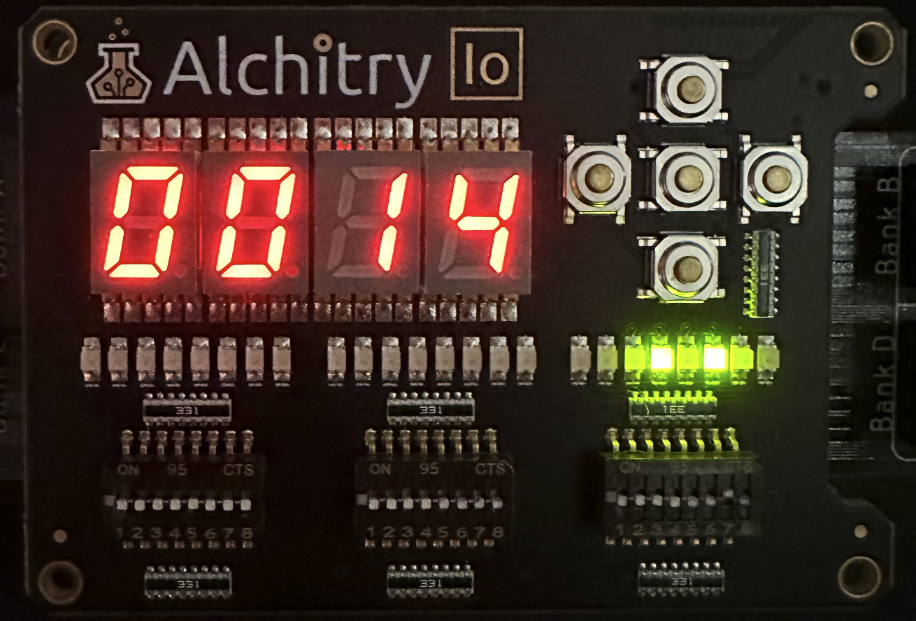
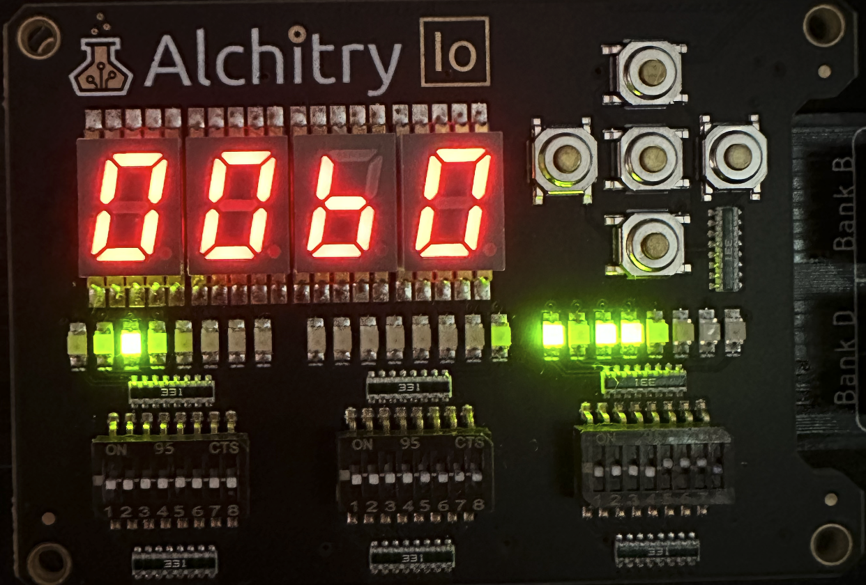
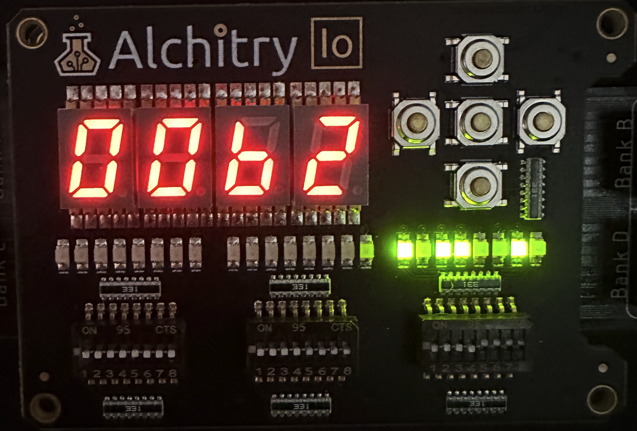
Press the top button (io_button[0]) and set io_dip[0]: 0xE. You should see b0 shown in the 7 seg immediately:
You can also press io_button[0] or io_button[1], and a different output is shown at the 7seg:
There’s nothing fancy at this moment. You’re simply viewing the content of system_input_buffer that stores current button presses immediately.
The irq handler
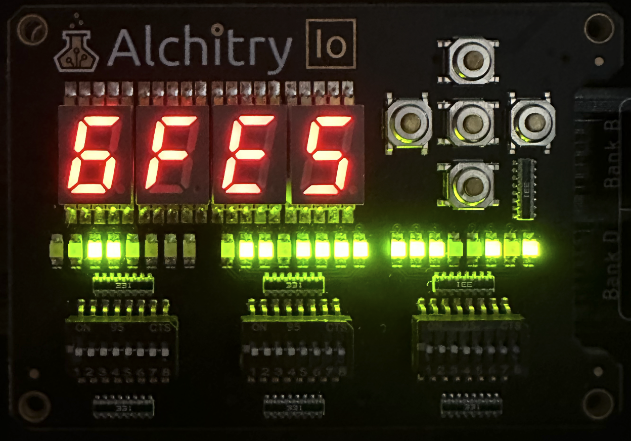
What’s interesting now is that if you press next, your ia (PC) will not execute the next address e.g (0x10 SUBC) but rather the irq handler entry at address 0x80000008.
Address 0x80000008 contains instruction BR(irq) where irq is at address 0x80000028, so pressing next will bring you there:
Let’s study what’s happening in the irq handler:
|| IRQ HANDLER, KERNEL PROGRAM ||
irq: LD(R31, 16, R4)	|| load hardwired value at input_buffer (Mem[16])
ST(R4, message, R31)	|| store (display) input value at output_buffer (Mem[12])
ADDC(R31, 12, R5)
JMP(R5)			|| jump to execute main program in user mode
|||||||||||||||||||||||||||||||||
At first, we load the content of Mem[0x10] to Reg[R4]. Remember that system_input_buffer is memory mapped to Mem[0x10] so what we are doing here is none other than loading the user input data to Reg[R4]. system_input_buffer should contain either 0xb0, 0xb1, or 0xb2 depending on which button you pressed.
Then we store the content of R4 to Mem[0xC]. Remember that system_output_buffer (which is equivalent to our monitors) is memory mapped to Mem[0xC] so our CPU can essentially store anything in this address 0xC to “output” whatever we want so that it can be seen by the output device.
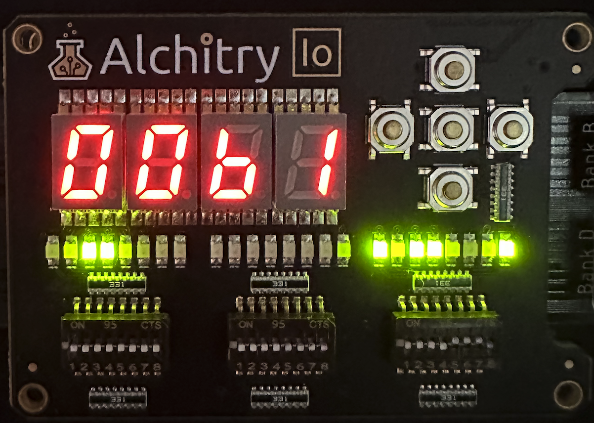
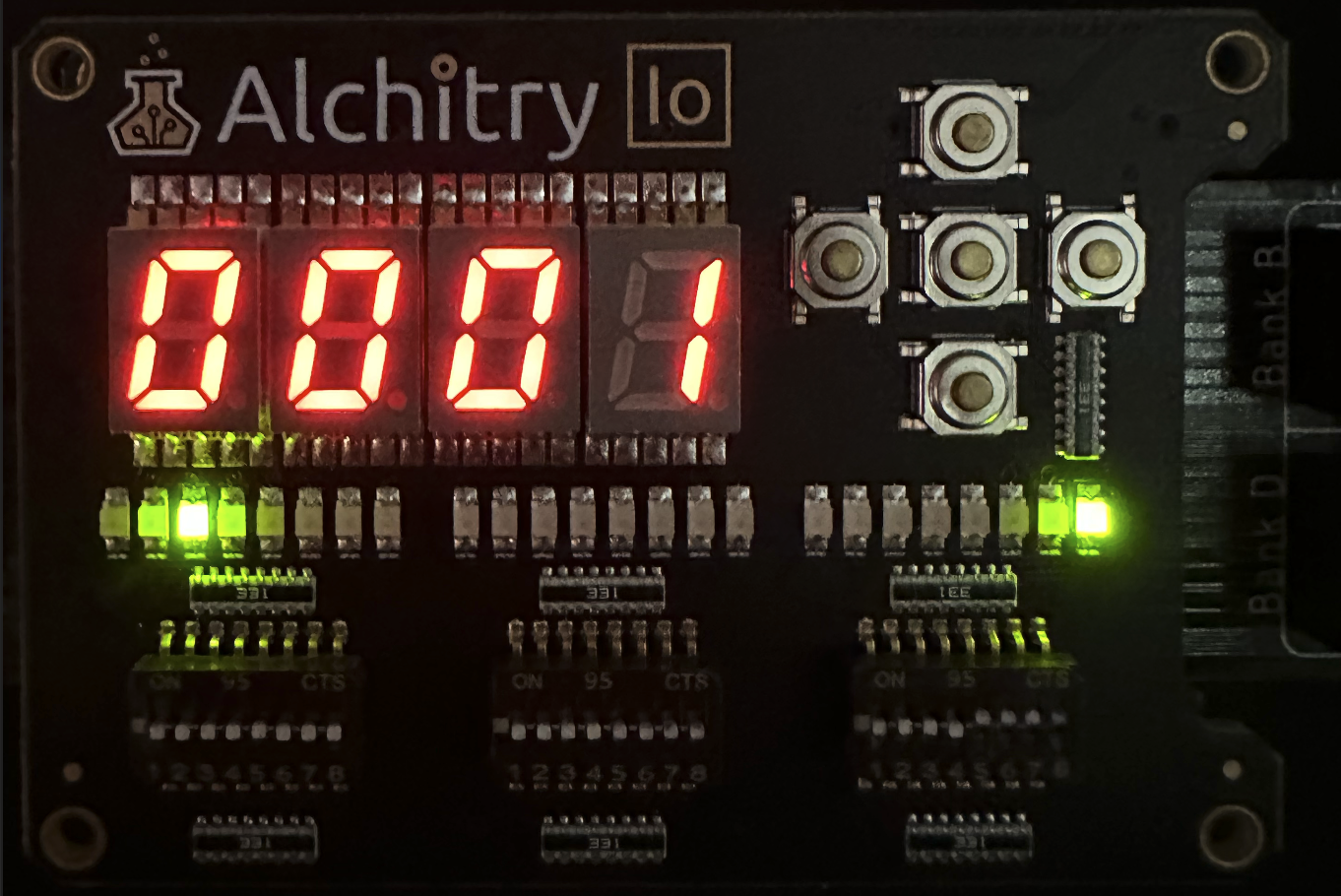
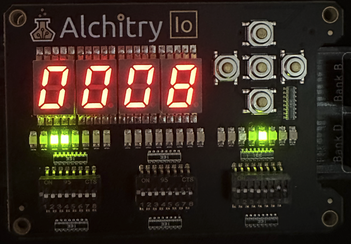
View it at this moment and confirm that its value is 0x01 due to the previous countdown 5, 4, 3, 2, 1 from triggering the illop handler:
Now, advance two more instructions until your current instruction address is 0x80000030.
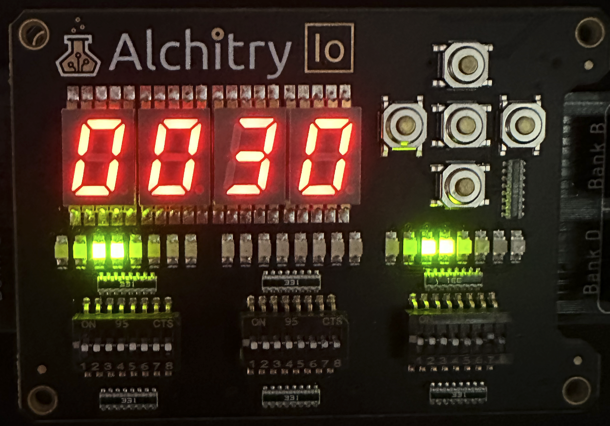
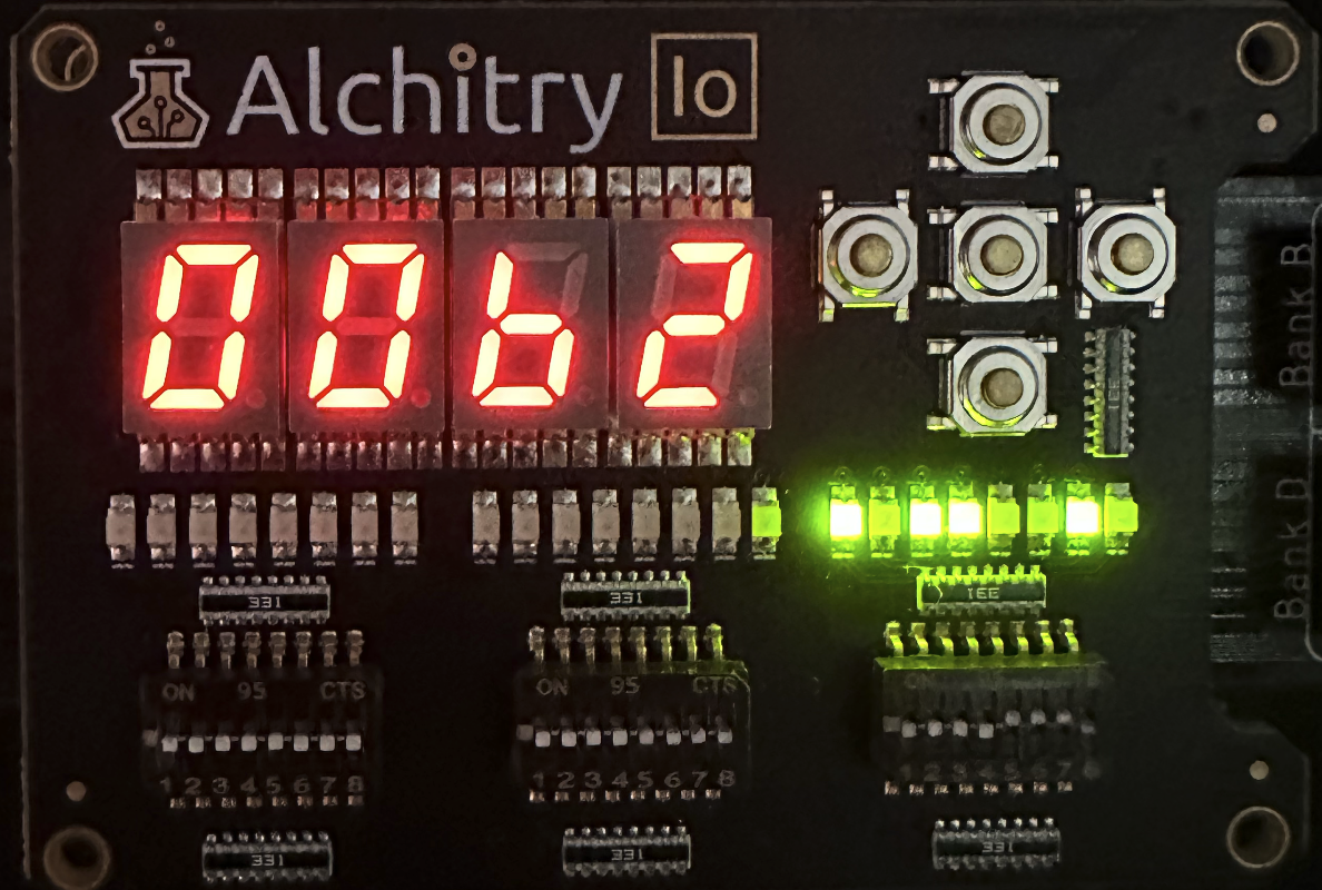
Then, view the state of system_output_buffer by setting io_dip[0]: 0xF. You should see the encoding of your last pressed button there:
Returning to main program in User Mode
The last two instructions of the irq handler ensures that we JMP back to address 0xC, which essentially restarts the main program.
You can prove this easily by advancing to address 0x034 (the last instruction of irq handler):
Confirm that it is indeed JMP(R5):
Then press next and it should bring you back to address 0xC:
Again, realise that you will be back at user mode by this point by viewing ia31 (set io_dip[0]: 0xD).
Problematic Return
Did you realise that initially we were about to execute address
0x14in user mode (main program), before the program got interrupted due to us pressing the input buttons, and yet we do not resume from0x14? We would expect our program to resume where it left off in the presence of hardware interrupt right?
If our programs don’t resume where it left off in the presence of (asynchronous) hardware interrupt, then our computers are not usable anymore. Imagine having our programs restart all the time at the event of any keyboard input or mouse movement or click.
The Solution
To know where to return to when user program is interrupted, we would save
PC+4value (that is address0x18in our example because PC was pointing to0x14when the program is interrupted) inReg[XP](R30). This is why we callR30a special register as its purpose is solely to store the return address of the last “paused” or interrupted instruction. You have used it a lot as well in Week 9 when you learn Stack and Procedure because it is used to store the return address after a function call exits.
Interrupt in Kernel Mode
Our Beta CPU should disable interrupt when we are currently handling an event (be it handling illop, or reset or another irq).
This is handled by the irq_sampler at the control unit:
    // sample interrupt at the beginning of each cycle
    if (~irq_sampler.q){
      // sample only when interrupt bit is 0 (clear)
      irq_sampler.d = irq;
    }
Plus the irq logic at the control unit:
    if (irq_sampler.q & slowclk & ~ia31){
      pcsel = b100;
      wasel = 1;
      werf = 1;
      wdsel = b00;
      wr = 0;
      // clear interrupt bit
      irq_sampler.d = 0;
    }
We check that irq cannot fire when ia31 == 1. However we do not “lose” the interrupt signal. irq_sampler dff was not reset to be 0 because the only way to clear it is by handling it.
We can demonstrate this very easily. Simply advance your Beta until you enter the illop handler. For the purpose of this example, we advance our PC until it points to address 0x8000003C (second instruction in illop handler). Ensure that your Beta CPU is in manual mode.
Then press io_button[1]. Ensure that this is immediately reflected at system_input_buffer:
Then press next. Notice that the next address of instruction to be executed is 0x80000040 and not the irq hander (0x80000008).
The entire illop handler will be executed up until the last instruction at address 0x064:
This will result in the Beta CPU returning to the user mode and its PC pointing to address 0x0C:
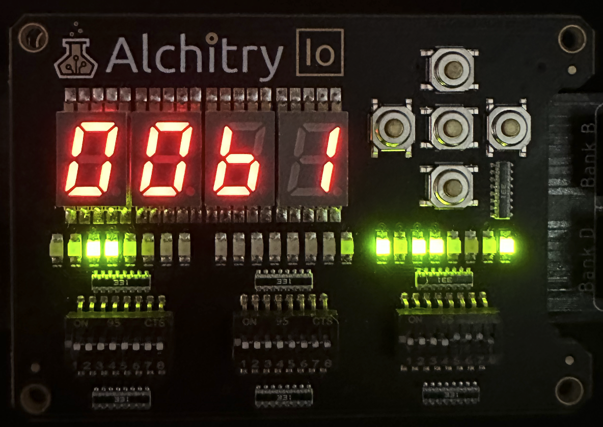
However, now our irq will take place. By pressing next, we are brought to the entry of the irq handler instead of the next address 0x10:
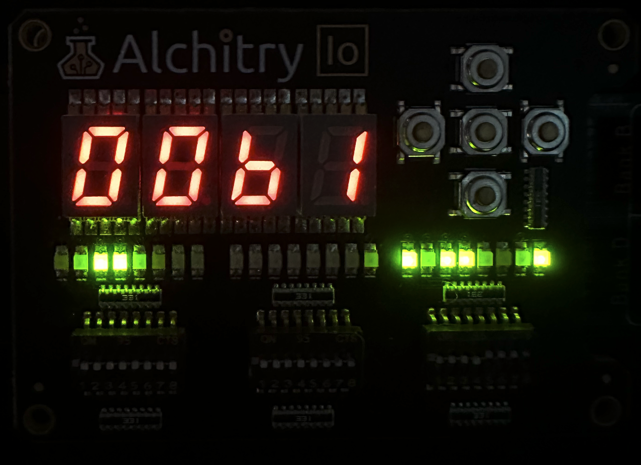
At this point, you will execute the entire sequence of irq handler and observe 00b1 at system_output_buffer eventually.
This short activity demonstrates that asynchronous interrupt (due to user input) is not necessarily “lost” even though we are in the midst of executing a program in Kernel mode (handling another event like illop). Of course, only the last input (before its handled) is captured because our system_input_buffer can only capture the last input. If we spam press the buttons while our Beta is running very slowly handling illop in Kernel mode, then earlier button presses will be lost and we only handle the final button press to be displayed at system_output_buffer.
In practice, this is tackled in three ways:
- Our CPU clock is extremely fast (>3 Ghz in 2023) such that it is humanly impossible to spam user inputs that fast. Our previous user input would have been processed by the
irqhandler before we can even supply another one. - Our Operating System Kernel will assign interrupt priority, so in practice we can interrupt our system in Kernel mode (provided contingency plans are in place so that we don’t lose our existing task). We will learn more about this at the end of this course and also in the first few weeks of 50.005.
- There exist smarter microcontrollers on our motherboard, and not just a simple
system_input_bufferlike what we have in this lab. They are capable of storing quite a bit of information and wait until our CPU is free to handle the interrupt event.
You need not to worry about the possibility that asynchronous interrupt request is lost at this point. Just now that eventually, all interrupt requests should be handled by our Operating System Kernel (which means you need to use a good kernel program coupled with decent hardware).
Summary
Experiment with different assembly program of your liking to ensure that you understand how Beta CPU works. You can even execute functions with proper procedure, or even use this as your 1D project.
Please talk to your instructors if you plan to implement your 1D with a general purpose CPU instead of an FSM. We would like to learn more about your implementation beforehand.
Also, be mindful about the supervisor bit. Ensure that you fully understand how it can be set or cleared. We paste the information from the first part of the handout below for clarity.
The highest-order bit of the PC (PC31/ia31) is dedicated as the supervisor bit (see section 6.3 of the Beta Documentation).
- The
LDRinstruction ignores this bit, treating it as if it were zero. - The
JMPinstruction is allowed to clear the Supervisor bit or leave it unchanged, but cannot set it, - No other instructions may have any effect on
PC31
The Beta CPU implemented in this lab is simplistic. We don’t have fancy stuffs as follows that provides abstraction and improves efficiency:
- Operating System Kernel
- Fancy I/O (keyboard, mouse)
- Virtual Address and Cache
However, hopefully this has shed some light to give you clarity on how our computers work and how they are constantly improved so that it can be the general-purpose devices we love today.