 50.002 CS
- Starter Code
- Related Class Materials
- Part 1 Introduction
- Task 1: Adder and Subtractor Unit
- Task 2: Compare Unit
- Task 3: Boolean Unit
- Task 4: Shifter
- Summary
50.002 Computation Structures
Information Systems Technology and Design
Singapore University of Technology and Design
Modified by: Natalie Agus (2024)
Lab 3: Arithmetic Logic Unit
Before this lab, you are required to complete this very basic FPGA tutorial we wrote and perhaps the official Getting-Started-With-FPGA tutorial by Alchitry lab. Please come prepared and bring your FPGA + laptops where Vivado + Alchitry Lab is installed. At least one person in each team should have a laptop that can run Vivado and bring the FPGA.
Starter Code
Please clone the starter code from this repository, then open it with Alchitry Lab.
git clone https://github.com/natalieagus/alu-starter.git
Since there’s only 1 FPGA per group, you need to work through this lab as a 1D group during class. However each person must still submit the lab questionnaire individually.
You are not required to submit your code for this lab. You will need it anyway for your 1D Project Checkoff 1: ALU and you should submit it then. Simply head to eDimension and do the lab questionnaire by the stipulated due date.
Related Class Materials
The lecture notes on Logic Synthesis and Designing an Instruction Set are closely related to this lab.
Part 1: Design 4 combinational ALU components
Related sections in the notes: Logic Synthesis
- N-input gates (all kinds of gates to produce the logic of each component in the ALU)
- Special combinational logic devices (multiplexer with 1 or 2 selectors, and combining multiplexers together to form an even bigger one)
The lab will reinforce your understanding on how you can build the circuit to conform to the logic that you want, e.g: adder circuit will perform binary addition of input A and B, etc, and make it programmable using the control signal: ALUFN.
You are NOT allowed to use any of Lucid’s math and comparison operators when implementing this lab’s ALU 13 functionalities. This is the requirement of your 1D project because we would like you to learn the basics and not solely rely on Vivado’s capability on creating components of the ALU. Please follow the implementation of the units from the given schematics. Failure to comply will result in -2% of your overall grades. However, you can use them for array indexing or checking conditions in loops.
Part 1 Introduction
In this lab, we will build a 32-bit arithmetic and logic unit (ALU) for the Beta processor. You will need this for your 1D Project Checkoff 1, just that you will need to modify it to be a 16-bit ALU. It should be a minor change for you to adapt the ALU for your 1D project (simply change in size). We will stick with 32-bit ALU in this Lab because we will need it for the next lab when we make the 32-bit Beta CPU taught in the lectures.
Arithmetic Logic Unit (ALU)
The ALU is a combinational logic device that has two 32-bit inputs (which we will call “A” and “B”) and produces one 35-bit output:
alu[31:0],Z,V, andN. We will start by designing the ALU modularly. It is composed from five as a separate modules, each producing its own 32-bit output. We will then combine these outputs into a single ALU result.
In this lab (both Part 1 and 2), we will attempt to create a 32-bit ALU. It is one of the components inside our Beta CPU. We will eventually utilise our work here to build an entire Beta CPU circuit in the next lab (Lab 4).
The Arithmetic Logic Unit (ALU) serves as the central core of the CPU, handling a variety of logical computations. Essential operations that a standard ALU encompasses are:
- An Addition/Subtraction Unit, facilitating elementary addition and subtraction tasks.
- A Comparison Unit, utilized for branching functions.
- A Boolean Unit, dedicated to boolean operations such as XOR, bit masking, and similar tasks.
- A Shifter Unit, instrumental in operations like division or multiplication by 2, as well as segmenting data.
- A Multiplier Unit, specialized in performing multiplication. The design of this unit is more complicated than the rest of the units. We will do this in Part 2 of the Lab, alongside assembling the complete 32-bit ALU.
Important: ALUFN != OPCODE
The
ALUFNsignal is NOT Beta CPUOPCODE, despite both being 6-bit long. These two encodings are NOT the same. TheALUFNis used to control the operation of the ALU circuitry, while the Beta CPUOPCODEis used by the Control Unit to control the entire Beta CPU datapath. In Lab 4, you will build a ROM as part of the Control Unit that will translate theOPCODEfield of a currently executed instruction into the appropriateALUFNcontrol signal.
Task 1: Adder and Subtractor Unit
Implement an adder/subtractor unit that can add or subtract 32-bit two’s complement (SIGNED) inputs (A[31:0], B[31:0]). It should generate a 35-bit output: (S[31:0]) andZ, V, N signals. A[31:0] and B[31:0] are the 32-bit two’s complement (SIGNED) input operands and S[31:0] is the 32-bit signed output. Z/V/N are the three other output code bits described below:
Zwhich is true when the S outputs are all zero (i.e.,NOR(S) == 1 ? Z = 1 : Z = 0)Vwhich is true when the addition operation overflows (i.e., the result is too large to be represented in 32 bits), andNwhich is true when the S is negative (i.e.,S31 == 1 ? N = 1 : N = 0).
Z, V, N will later be used by the comparator unit (read next section). The following diagram illustrates a suggested implementation of the 32-bit Adder/Subtractor Unit using a Ripple Carry Adder (RCA):
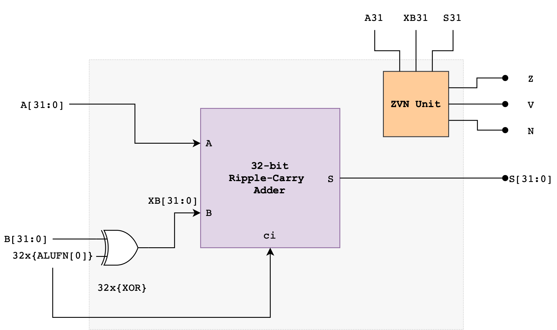
The ALUFN0 input signal controls whether the operation is an ADD or SUBTRACT. ALUFN0 will be set to 0 for an ADD (S = A + B) and 1 for a SUBTRACT (S = A – B). To perform a SUBTRACT, the circuit first computes the two’s complement of the B operand before adding the resulting value with A. The two’s complement of B is computed using the XOR gate and ALUFN0 as carry in to the first Full Adder in the RCA.
Computing Overflow: V
Note that overflow can never occur when the two operands to the addition have different signs. If the two operands have the same sign, then overflow can be detected if the sign of the result differs from the sign of the operands. Note that we use XB, not B.
Think!
Why is
Vcomputed like the above? Start by having a small example, let’s say a 4-bit RCA. If we haveA: 0111, andB: 0001, adding both values will result in a positive overflow. The true answer to this should be decimal8. With signed devices, we need 5 bits to represent decimal 8:01000. However since our RCA can only output 4-bits, we have our output as just1000, and this means decimal -8 in a signed 4-bit output. Now think about other possible overflow cases (negative overflow, etc).
Detailed Adder/Subtractor Schematic
Here’s the detailed schematic of the adder to get you started:
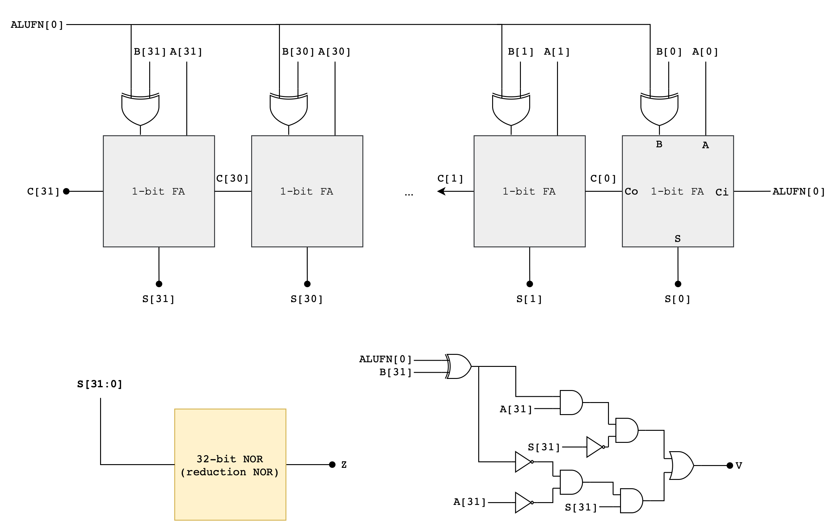
You may start by making a 1-bit Full Adder module first, and then create a 32-bit RCA module. Afterwards, assemble everything inside adder.luc.
Implementation Tips
Remember that you are NOT allowed to use Lucid’s math operator, such as out = a+b or out = a-b to implement the adder unit. Please follow the implementation of the schematic above. This is part of the requirements of your 1D project. You can however use these operators for indexing.
for-loops
You can utilise for loops in Lucid (the same applies for Verilog) to duplicate creation of multiple units of fa. For instance, if you have the following fa module interface:

// fa.luc
module fa (
    input a,
    input b,
    input ci,
    output co,
    output s
  )(
    // implementation

  )
You can utilise it as follows to create a 32-bit Ripple Carry Adder module’s body:
// rca.luc
module rca (
    input a[32],
    input b[32],
    input ci,
    output s[32]
  ) {
  fa fa[32];
  var i;

  always {

    // set the inputs to the first unit (LSB) of the RCA
    fa.a[0] = a[0];
    fa.b[0] = b[0];
    fa.ci[0] = ci;

    for (i=1; i<SIZE; i++){ // define the connections for the other 31 units of fa
      fa.a[i] = a[i];
      fa.b[i] = b[i];
      fa.ci[i] = fa.co[i-1];
    }

    s = fa.s; // connect the output bits
  }
}
Remember that for-loops in HDL (Hardware Design Language) like Lucid or Verilog does not perform the same way like the for loops we are familiar with in Python or Java. It’s important to understand that in HDLs, for-loops are used to describe hardware, not to control flow as in software programming. They primarily for generating repetitive hardware structures.
Reduction Operators
In HDLs, reduction operators applies the logic across the bits of the input to produce a single bit output. For instance, given a = 4b1010:
|a(reduction OR) is1|0|1|0, which is1&a(reduction AND) is1&0&1&01which is0^a(reduction XOR) is1^0^1^0which is0
Test
Once you have implemented adder.luc, connect its input and output properly in alu.luc so that we can test our adder unit manually.
// alu.luc body
    adder.a = a;
    adder.b = b;
    adder.alufn_signal = alufn_signal;

    z = adder.z;
    v = adder.v;
    n = adder.n;

    out = adder.out;
Afterwards, compile the project and test them using the dip switches and observe the output at io_led. We have written a simple test connection for you. You can press io_button[0] to capture the current dip switches state as the value of a, io_button[1] as the value of b, and io_button[2] as the value of alufn. The “captured” value will be whatever the state of the dip switches is during the press.
Since a and b are 32-bit long and we only have 24 dip switches, we took a shortcut and encode the following:
  // store a
  a.d = c{io_dip[2], 8b0, io_dip[1], io_dip[0]}; // set io_dip[2] to dictate MSB 8 bits
As for alufn signal, we use io_dip[0][5:0] (the rightmost 6 switches).
Think of useful test cases, such as addition of zeroes, addition of two negative numbers, test overflow, subtraction of -ve values, and so on.
Please utilise the switches carefully, they’re delicate and easy to break. Use the tip of a male jumper wire to flick them.
Further Note
We made it a requirement in your 1D project to NOT use Lucid (or Verilog) math and comparison operators when implementing any of the 13 functionalities of the ALU. You can technically implement a 32-bit adder unit in this manner and let Vivado do the work:
module adder (
    input a[32],
    input b[32],
    input alufn0,
    output s[32]
  ) {

  always {
    if (alufn0){
      s = a + b;
    }
    else{
      s = a - b;
    }
  }
}
However the above does not allow you to learn anything new. Implementing components of the ALU from scratch has its own benefits as you’re still learning.
Firstly, it enables you to gain a deeper insight into the underlying hardware mechanisms that perform arithmetic operations, and offers a tangible perspective on how abstract mathematical concepts are translated into physical, operational circuits.
This hands-on experience is invaluable for developing an appreciation of the intricacies and challenges associated with digital circuit design, including considerations of timing, power consumption, and scalability.
Secondly, it encourages problem-solving skills, requiring you to apply logic and reasoning to create efficient and functional circuits, along with the first few weeks of 50.002 materials. This process enhances your ability to design, troubleshoot, and optimize digital systems, skills that are crucial for both academic and professional success in the CS field.
Finally, it cultivates an appreciation for the evolution of digital design methodologies and the role of automation in modern engineering. You are not learning how to rely on Vivado but rather to figure out how it works under the hood.
Task 2: Compare Unit
Implement a 32-bit compare unit that generate 1 bit output, depending on the following conditions:
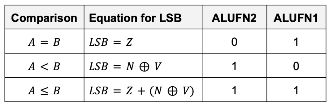
The inputs to the compare unit are:
- The
ALUFNcontrol signals (used to select the comparison to be performed), in particular:ALUFN[2:1] - The
Z,V, andNbits. They’re the output of the adder/subtractor unit. The adder must be in subtraction mode.
Think!
Why should the adder be in subtraction mode?
Performance
The Z, V and N inputs to this circuit can only be produced by the adder/subtractor unit. That means we need to first perform a 32-bit addition/subtraction between a and b before we can compare them. This means there’s some significant tpd to produce the output of the compare unit as the RCA is considerably slow.
In real life, you can speed things up considerably by thinking about the relative timing of Z, V and N and then designing your logic to minimize delay paths involving late-arriving signals. For instance, if you need to perform computations involving Z and other variables, you can compute those intermediary output involving the other variables first while “waiting” for Z. We do not need to worry much about it in this Lab as Vivado will do all sorts of optimisation for you.
Detailed Compare Unit Schematic
Here’s the detailed schematic of the compare unit. Pay close attention to the bit selector and the corresponding inputs at the mux:
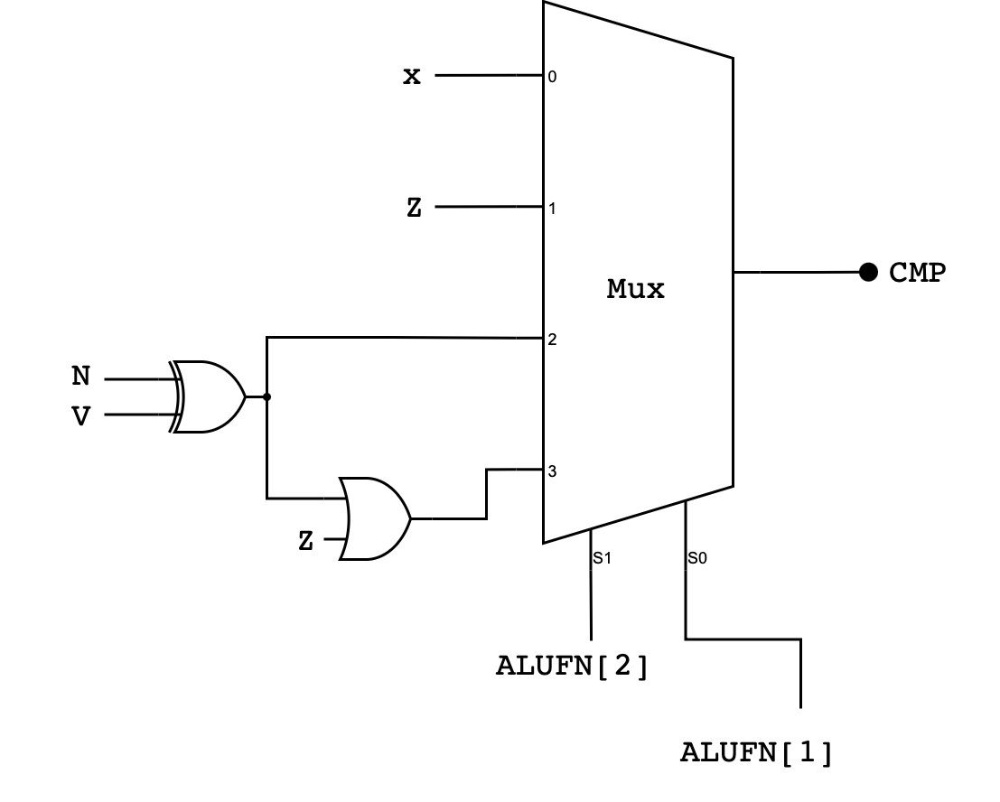
Implementation Tips
Since you are not allowed to use Lucid’s math and comparison operators to implement this lab, it will be beneficial for you if you create a mux_4 unit first:
// mux_4.luc
module mux_4 (
    input s0,  // selectors
    input s1,
    input in[4], // inputs
    output out
  ) {

  always {
    case (c{s1, s0}){
      b00: out = in[0];
      b01: out = in[1];
      b10: out = in[2];
      b11: out = in[3];
      default:
        out = 0;
    }
  }
}
You can then utilise this inside compare.luc to implement the compare truth table above.
Test
Test your compare unit manually before proceeding to the next section.
- Edit
alu.lucand make all the necessary connection between theadderand thecompareunit, - Supply the
Z, V, Ninputs to thecompareunit appropriately, - Set
adder.alufn_signal = 1as the adder must be subtracting in order for theZ, V, Nsignal to be usable by the compare unit
You should connect the out signal of alu.luc to the output of the compare unit instead of the adder unit for now.
Since the alu must produce a 32-bit output, you should set the higher 31 bits to 0, and set the LSB to the output of the compare unit as follows:
// alu.luc body
  out = c{31x{b0}, compare.cmp}; // concatenation
Again, your test cases must be comprehensive, and think of possible edge cases such as comparing two negative numbers together, or comparing zeroes.
It is very important to test each of your modules incrementally before proceeding to the next section. Debugging HDL is extremely difficult (no straightforward and convenient print statements or debugger to “pause” execution), so we shall minimise propagation of errors by testing each small module carefully.
Task 3: Boolean Unit
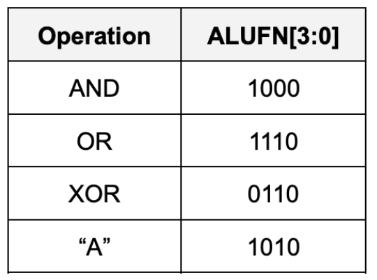
Implement a 32-bit Boolean unit that performs bitwise boolean operation between a and b. The unit should receive 32-bits of a and b as inputs, as well as 4-bit ALUFN[3:0] input, and produce a 32-bit output. In particular it should perform either AND, OR, XOR, or A bitwise boolean operations, depending on the ALUFN signals supplied:
Detailed Boolean Unit Schematic
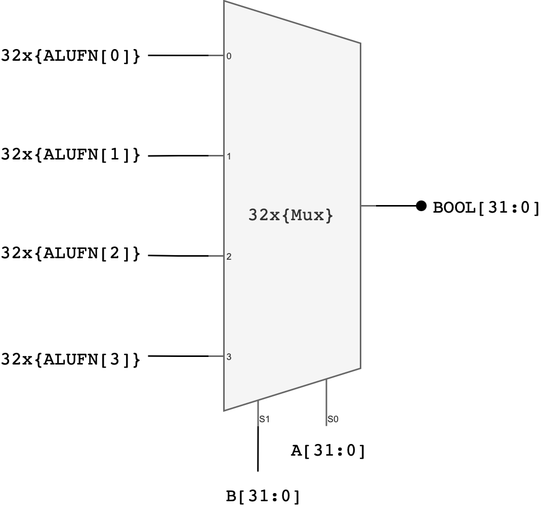
Here’s the general schematic of the Boolean Unit:
Explanation:
One possible implementation of a 32-bit boolean unit uses 32 copies of a 4-to-1 multiplexer where ALUFN0, ALUFN1, ALUFN2, and ALUFN3 hardcode the operation to be performed, and Ai and Bi are hooked to the multiplexer SELECT inputs. This implementation can produce any of the 16 2-input Boolean functions; but we will only be using 4 of the possibilities: AND, OR, XOR, and A.
In total, you should utilise 32 4-to-1 multiplexers to build the boolean unit. You can utilise the earlier created mux_4.luc module to implement this.
Implementation Tips
You will need 32 copies of ALUFN signals as you will be plugging them into the input ports of each mux_4. To do this, you can use the duplication operator in lucid, for instance:
// boolean.luc
  // module declaration

  // declaration of modules utilised in boolean unit
  mux_4 mux_4_32[32];

  always{
    // create 32 copies of ALUFN signal as input to each mux_4 unit
    // the double curly brackets are intentional because
    // we are creating 2D array: 32 by 4 bits
    mux_4_32.in = 32x{{alufn_signal[3:0]}};
    // the rest of boolean.luc body

  }
Test
Please test the boolean.luc module by making appropriate connections in alu.luc before proceeding. For now, connect the output of the boolean unit to the output of the alu unit, as follows:
// alu.luc body

  boolean.a = a;
  boolean.b = b;
  boolean.alufn_signal = alufn_signal;

  out = boolean.bool
Don’t forget to think of useful test cases that test not only the functionality of each boolean operation, but also edge cases (e.g: A and B are all 0 or 1).
Task 4: Shifter
Implement a 32-bit shifter unit that is able to perform a shift left (SHL), shift right (SRA), or shift right arithmetic (SRA) operation on A:
- The
A[31:0]input supplies the data to be shifted - The low-order 5 bits of the
B[4:0]are used as the shift count (i.e., from 0 to 31 bits of shift) - We do not use the high 27 bits of the
Binput (meaning thatB[31:5]is ignored in this unit)
For example, if A: 0x0000 00F0 and we would like to shift A to the left by FOUR bits, the B input should be 0x0000 0004
The desired operation will be encoded on ALUFN[1:0] as follows:
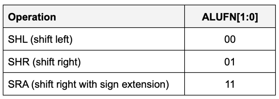
With this encoding, the control signal ALUFN0 controls whether we are performing a left shift or a right shift (SHR). ALUFN1 decides whether we apply the sign extension logic on right shift.
- For
SHLandSHR,0s are shifted into the vacated bit positions. - For
SRA(“shift right arithmetic”), the vacated bit positions are all filled withA31, the sign bit of the original data so that the result will be the same as arithmetically dividing the original data by the appropriate power of 2.
Detailed Shifter Unit Schematic
The simplest implementation is to build three separate shifters: one for shifting left, one for shifting right, and one for shifting right arithmetic.

Notice how a multi-bit shift can be accomplished by cascading shifts by various powers of 2.
- For example, a 13-bit shift can be implemented by a shift of 8, followed by a shift of 4, followed by a shift of 1.
- Each shifter unit is just a cascade of multiplexers each controlled by one bit of the shift count.
Afterwards, we can use a 4-way 32-bit multiplexer to select the appropriate answer as the unit’s output.
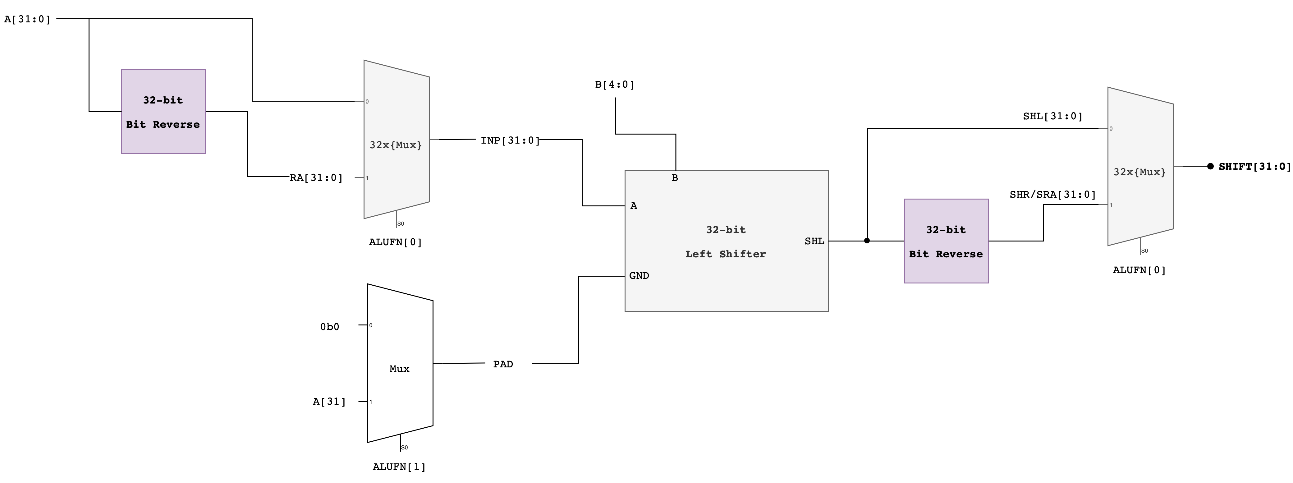
Alternative Approach: Compact Shifter
Another approach that adds latency but saves gates is to use the left shift logic for both left and right shifts, but for right shifts, reverse the bits of the
Ainput first on the way in and reverse the bits of the output on the way out.Here’s the schematic of this compact shifter.
Implementation Tips
You might want to create a mux_2.luc module here to help your implementation:
module mux_2 (
    input s0,
    input in[2], // note: you can put input as an array, or declare them separately, e.g: input d0, input d1
    // it will affect how you utilise this mux
    output out
  ) {

  always {
    case (s0) {
      0: out = in[0];
      1: out = in[1];
      default:
        out = 0;
    }
  }
}
Then, you might want to implement x_bit_left_shifter.luc unit, where x is a variable value. You can supply a parameter to a module that can be “instantiated” during declaration time.
module x_bit_left_shifter #(
  // parameter declaration, to be set during module instantiation
  // default value given is 8
  SHIFT = 8 : SHIFT > -1 & SHIFT < 32
  )(
    input a[32],
    input shift,
    input pad,
    output out[32]
  ) {

  // module declarations
  // declare your mux_2 (32 of them)
  // other useful variables, e.g: shifted_bits[32]

  always {
    // assign value to shifted_bits[32] depending on the value of SHIFT
    // connect the selector of each mux_2 with shift
    //
    // use a for-loop to:
    // connect input[0] of each mux_2 with a[i]
    // connect input[1] of each mux_2 with the shiftedbits[i]xs
  }
}
Warning: Instance Connections
Be cautious when connecting inputs and parameters using instance connections. They are duplicated across modules.
For example:
pipeline pipe [8] (#DEPTH(16));instantiate 8 pipe modules, each withDEPTH = 16. As of now, we have not find a direct way to set differentDEPTHparameter values for eachpipe(in verilog, we can do this withgenerate).Here’s what the documentation say: You can also specify an array size for the instance. If you do this, that module will be duplicated in your design for each element in the array. Any connections or parameters specified at instantiation will be connected to each instance separately. For example, if your module has a single-bit input
clkand you connect a signal to it, that single-bit signal will be duplicated and connected to each module.However, this behaviour is not observed in
dff(special type). You can do:dff ctr [32] (#INIT(32d15), .clk(clk));andctr[0]will take the least significant bit of32d15asINIT, which is1, andctr[31]will take the most significant bit of32d15as itsINIT, which is0.
Performance
The shifter unit is made by cascading various multiplexers together to shift A in stages. Suppose you know the tpd of each mux_2, could you compute the tpd of the shifter unit output?
Of course it depends on your design and which shift operation is done (e.g: SHR vs SRA). Compute the
tpdfor each design (regular vs compact shifter) and shift operation.
Test
Please test the shifter.luc module by making appropriate connections in alu.luc before proceeding. For now, connect the output of the shifter unit to the output of the alu unit, as follows:
// alu.luc body

  shifter.a = a;
  shifter.b = b[4:0];
  shifter.alufn_signal = alufn_signal;

  out = shifter.shift;
Please be mindful when testing this unit, it should be as comprehensive as the tests you’ve done for the other 3 units above.
Summary
You are free to implement each module in whichever way you deep fit, or even come up with a new schematic as long as you don’t use Lucid’s math operators and compare operators to implement any of these 13 functionalities. You can however use them for indexing purposes or conditional loops.
Remember to always test each module separately.
In the next lab, we will implement the multiplier module and attempt to assemble each module together to form a complete 32-bit ALU unit.
When you’re done with the implementation of these 4 modules, head to eDimension to complete this week’s lab quiz.