 50.002 CS
- Starter Code
- Related Class Materials
- Introduction
- Memory Unit
- Part A: PC Unit
- Part B: REGFILE Unit
- Part C: CONTROL Unit
- ALU + WDSEL Unit
- Part D: Assemble Completed Beta
- Compile and Run
- Observed Output
- A Better Test Instruction
- What’s Next?
50.002 Computation Structures
Information Systems Technology and Design
Singapore University of Technology and Design
Written by: Natalie Agus (2023)
Lab 4: Beta Processor with FPGA (Part 1)
Starter Code
Please clone the starter code from this repository, then open it with Alchitry Lab.
git clone https://github.com/natalieagus/beta-starter.git
Then, you shall paste the implementation of your 32-bit ALU unit created in Lab 3: ALU. Be sure to include all files required by your alu.luc.
Since there’s only 1 FPGA per group, you need to work through this lab as a 1D group during class and obtain checkoff as a group by the end of the Lab next week. However each person must still submit the lab questionnaire individually. For the checkoff next week, only group members who are present gain the marks (unless valid LOA).
You are not required to submit your code for this lab, only to show your implementation to your TA and instructors by the end of the Lab next week. Simply head to eDimension and do the lab questionnaire by the stipulated due date.
Related Class Materials
The lecture notes on Building the Beta CPU, and Designing an Instruction Set are closely related to this lab.
This lab will reinforce your understanding on how the Beta CPU works, and all data paths for OP, OPC, Control Transfer, and Memory Access operations.
Related sections in Designing an Instruction Set:
- The Von Neumann model: CPU, Memory, IO
- Programmability of a Von Neumann Machine: basics of programmable control systems (using control signals like
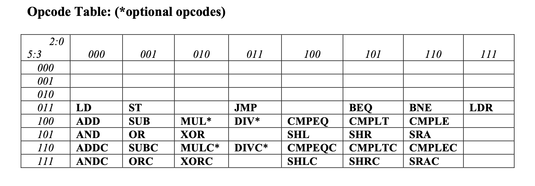
OPCODEto activate different data paths in the Beta CPU). - Beta ISA Format
- Beta Instruction Encoding
Related sections in Beta CPU:
- OP datapath
- OPC datapath
- Memory Access datapath
- Control transfer datapath
- Interrupt handling
- By the end of this lab, you should know how to build the schematic of the entire Beta CPU based on its ISA (blueprint). This lab will also help you to familiarise yourselves with core Beta instructions
Introduction
The goal of this lab is to build a fully functional 32-bit Beta Processor on our FPGA so that it could simulate simple programs written in Beta Assembly Language. It is a huge device, and to make it more bearable we shall modularise it into four major components:
- (Part A) PC Unit: containing the PC register and all necessary components to support the ISA
- (Part B) REGFILE Unit: containing 32 32-bit registers, WASEL, and RA2SEL mux, plus circuitry to compute Z
- (Part C) CONTROL Unit: containing the ROM and necessary components to produce all Beta control signals given an
OPCODE - ALU+WDSEL Unit: containing the ALU and WDSEL, ASEL, BSEL muxes (given to you)
- (Part D) Assemble the entire Beta CPU using all subcomponents above
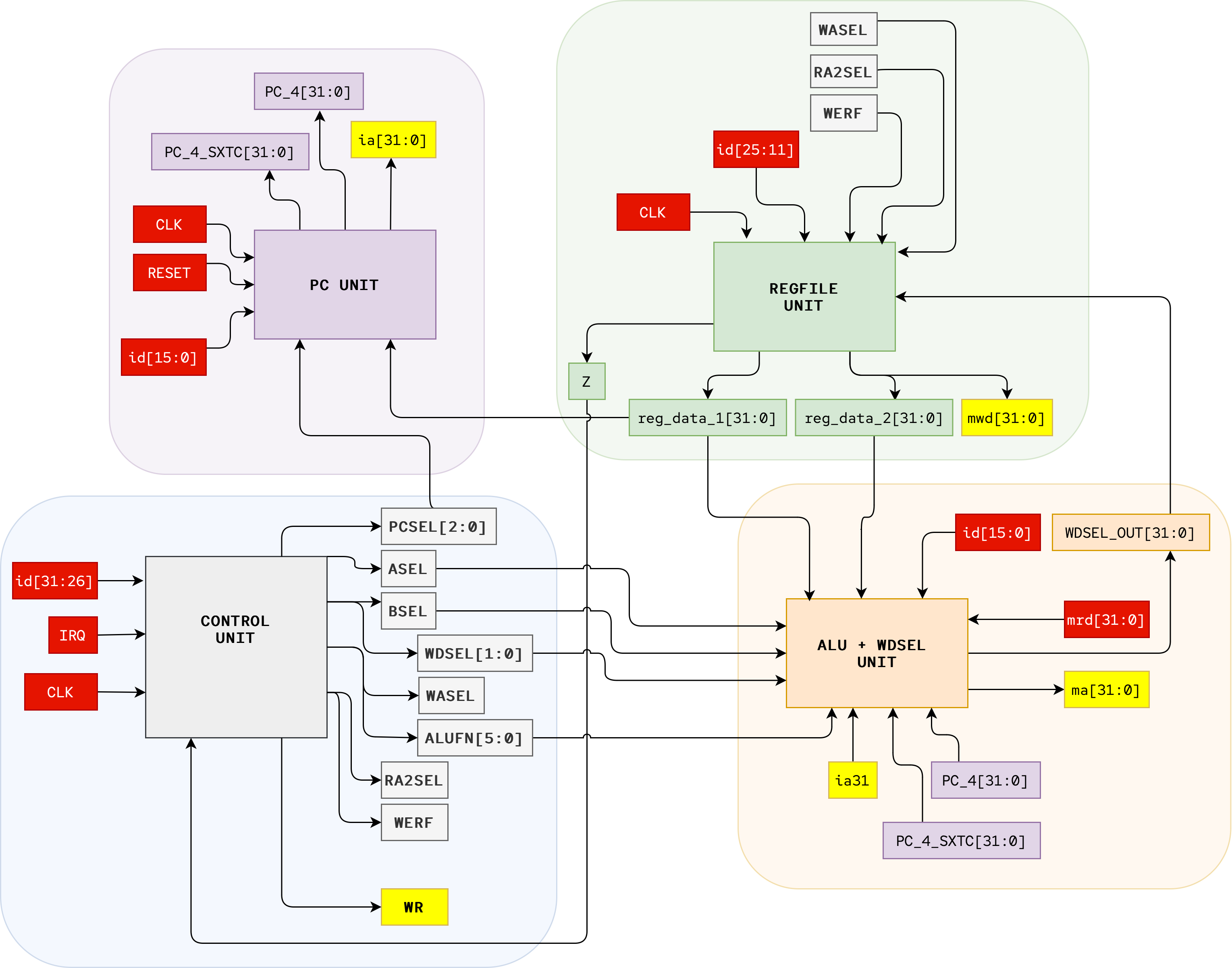
The signals indicated in red refers to external INPUT to our Beta, supplied by the Memory Unit. The signals illustrated yellow refers to our Beta’s OUTPUT to the Memory Unit.
Please study each section carefully as this will be beneficial not only for your 1D Project and Exam, but also to sharpen your knowledge in basics of computer architecture which might be useful in your future career as a computer science graduate.
Memory Unit
The Memory Unit is implemented in the file memory_unit.luc. It is physically separated into two sections for ease of explanation and implementation:
- the instruction memory and
- the data memory
In practice, the data segment of the memory and the instruction segment of the memory is only logically segregated. They still share the same physical device we know as RAM.
The schematic of the memory unit is as follows:
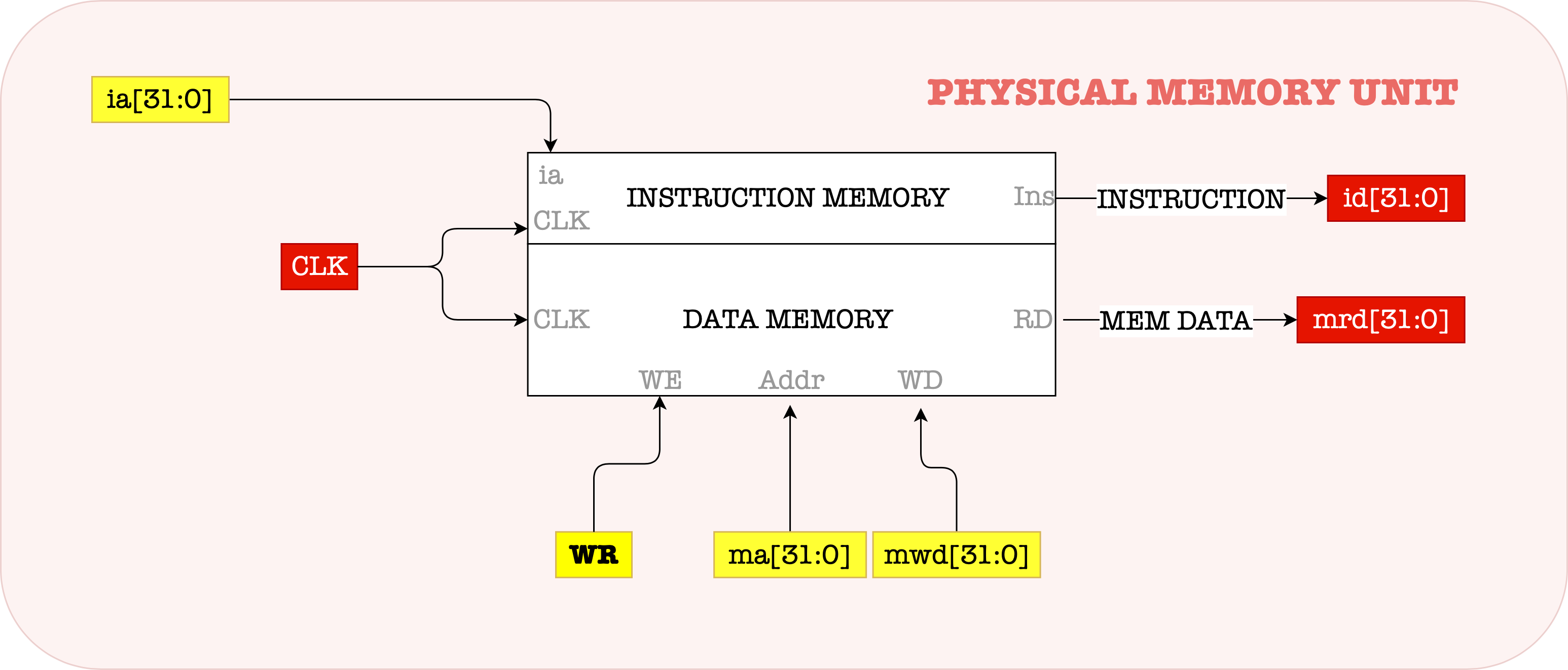
Instruction Memory
The instruction memory is implemented using the simple_ram.v component. See this file under the Components folder in your alchitry project to read more about how to use it. In short:
read_dataport of thesimple_ramwill output the value of the entry pointed byraddrin the previous clock cycle. If you want to read addressEA, you shall setraddr = EAand then wait for one FPGA clock cycle forMem[EA]to show up.- If you read and write to the same address, you will get the value of the old output at
read_datain the second clock cycle, and on the third clock cycle, the newly updated value will be produced atread_data.
The input to the instruction memory supplied by the Beta is: instruction address (ia[31:0]). This contains the address of the next instruction to be executed. This will cause the instruction memory to output instruction data (id[31:0]) for the Beta CPU. Since we never need to write to this instruction memory during program execution, we implement it as a single port ram (only read or write can be done one at a time in one clk cycle)
The instruction memory unit receives input address ia[31:0] and outputs instruction data id[31:0]. After a certain propagation delay, the memory unit will supply the Beta with the contents of address ia[31:0]. We symbolically illustrate this content as Mem[EA], where EA = ia[31:0].
The interface of the instruction memory is given to you inside memory_unit.luc:
    // for instruction memory
    input ia[$clog2(WORDS)+2], // byte addressing expected
    input instruction_write_enable,
    input instruction_towrite[32],
    output id[32]
Data Memory
The Beta CPU can read or write to the Data Memory. For ease of demonstration data memory is implemented as a dual port ram (read and write can be done independently in the same clk cycle). That is why we have two address ports raddr and waddr inside memory_unit.luc instead of addr like illustrated in our diagram above, but in principle they work the same way. See simple_dual_ram.v in the Components folder in your Alchitry project for more information. In short:
read_dataport of thesimple_ramwill output the value of the entry pointed byraddrin the previous clock cycle. If you want to read addressEA, you shall setraddr = EAand then wait for one FPGA clock cycle forMem[EA]to show up.- We should avoid reading and writing to the same address simultaneously because the
read_datawill be undefined.
The interface for the data memory is given to you inside memory_unit.luc:
    // for data memory
    input raddr[$clog2(WORDS)+2], // byte addressing expected
    input waddr[$clog2(WORDS)+2], // byte addressing expected
    input wd[32], // write data
    input we,
    output mrd[32],
Memory Read
The Data Memory Unit receives one input from the Beta:
- data memory address (
ma[31:0]). This is the address of data memory location where we want to read (load) from or write (store) to. - We often know this as
EAin our lecture notes as well.
When the Beta wants to load (read) data from the memory, it needs to supply the above ma[31:0] to the memory unit. Then, the data memory will output mrd[31:0] (otherwise known as Mem[EA]) for the Beta CPU.
Memory Write
If the Beta wants to store (write) data to the memory, it needs to supply two signals to the data memory:
- memory write data (
mwd[31:0]): the 32-bit data to be stored to the memory unit, and, - memory write enable (
wr) signal. Set to 1 when the Beta wants to store into the memory location specified byma[31:0]at the end of the current cycle.
The signal wr should ALWAYS have a valid logic value (either 1 or 0) at the RISING edge of CLK otherwise the contents of the memory will be affected. If signal wr is 1, the data mwd[31:0] will be written into memory at the end of the current cycle. Otherwise, if wr = 0, then the data at mwd[31:0] will be ignored.
Addressing Convention
We expect byte addressing to be supplied at raddr, waddr, and ia. However, since we would naturally declare our simple_ram with #SIZE(32), it expects word addressing. Hence, we need to ignore the lower two bits of ia, raddr, and waddr when using them.
instruction_memory.address = ia[$clog2(WORDS)+2-1:2];
Given memory capacity of WORDS, we need to take log2 of it to find the minimum number of bits to address this many WORDS of data. When declaring ia, we state that ia contains $clog2(WORDS)+2 bits. Thus when indexing, we want to start from index $clog2(WORDS)+2-1 (this is MSB). Since we only want word addressing when actually using the simple_ram, we simply start from index $clog2(WORDS)+2-1 and end at index 2 (inclusive).
Note that we can declare our simple_ram with #SIZE(4), #DEPTH(WORDS*4) if we want it to strictly be byte addressable, but we will need additional logics to extract 4 bytes at a type.
Part A: PC Unit
PC Unit Schematic
Here is the suggested PC Unit schematic that you can implement. Take note of the input and output notes. This will come in very useful when creating the module for your PC Unit.
Task 1: PCSEL Multiplexers
Implement the PCSEL mux section inside pc_unit.luc. You can follow the following guide, and read each of its relevant sections below.
    case (pcsel){
      // consider all cases of pcsel signals
      // for JMP, make sure to compute the supervisor bit properly
      // for ILLOP and IRQ handlers, ensure that the supervisor bit is set to 1

      default: // just a default case to silence warnings
        pcsel_out_sig = pc.q;
     }

    // advance the PC only when slowclk is 1
    if (slowclk){
      // set the content of pcreg to be its next value only when slowclk == 1

    }
The 32-bit 5-to-1 PC mux selects the value to be loaded into the PC register at the next rising edge of the clock depending on the PCSEL control signal.
XAddr and ILLOP
XAddr and ILLOP in the Beta diagram in our lecture notes represents constant addresses used when the Beta services an interrupt (triggered by IRQ) or executes an instruction with an illegal or unimplemented opcode. For this assignment assume that XAddr = 0x80000008 and ILLOP = 0x80000004 and we will make sure the first three locations of main memory contain BR instructions that branch to code which handle reset, illegal instruction traps and interrupts respectively. In other words, the first three locations of main memory contain:
Mem[0x80000000] = BR(reset_handler)
Mem[0x80000004] = BR(illop_handler)
Mem[0x80000008] = BR(interrupt_handler)
Lower Two Bits of PC
You also have to force the lower two bits of inputs going into the PC+4, PC+4+4*SXTC, and JT port of the mux to be b00 because the memory is byte addressable but the Beta obtains one word of data/instructions at each clock cycle. You can do this with appropriate wiring.
Example:
pc.d = c{pcsel_out[31:2], b00};
Task 2: RESET Multiplexer
Implement the RESET multiplexer in the space provided under RESET mux section inside pc_unit.luc.
Remember that we need to add a way to set the PC to zero on RESET. We use a two-input 32-bit mux that selects 0x80000000 when the RESET signal is asserted, and the output of the PCSEL mux when RESET is not asserted.
We will use the RESET signal to force the PC to zero during the first clock period of the simulation. This can be found inside motherboard.luc:
// motherboard.luc

   case(motherboard.q){
        // instruction loading
        motherboard.INSTRUCTIONLOAD:
            beta.rst = 1;
            writer_counter.d = writer_counter.q + 1;
            instruction_unit.addr = writer_counter.q;
            memory_unit.instruction_towrite = instruction_unit.out;
            memory_unit.instruction_write_enable = b1;
            memory_unit.ia = writer_counter.q<<2; // pad with two zeroes to make it byte addressable because memory_unit expects byte addresing ia
            if ((writer_counter.q + 1) == MEMORY_SIZE){
                motherboard.d = motherboard.RUN; // wait one more clock cycle to allow the last instruction to be loaded before start execution
        }

         motherboard.RUN:
            // only load output and update input at the the beginning of each "next" instruction cycle
            // LOAD_OUTPUT will hijack EA for 2 cycles. At this point, the CPU is not receiving a legitimate Mem[EA] if it is doing a LD/LDR
            // However since "next" is more than 2 cycles, it will be fixed by the third cycle (actual EA coming out from beta is plugged into memory unit
            if (slowclk){
                motherboard.d = motherboard.LOAD_OUTPUT;
            }
            else{
                motherboard.d = motherboard.RUN;
            }
      ...
Task 3: 32-bit PC Reg
The PC is a separate 32-bit register that can be built using the dff component. We have declared it above the always block:
dff pc[32](#INIT(0),.clk(clk)); // PC Register
Increment-by-4
Conceptually, the increment-by-4 circuit is just a 32-bit adder with one input wired to the constant 4. It is possible to build a much smaller circuit if you design an adder optimized knowing that one of its inputs is 0x00000004 constant. In Lucid, this can be done very easily by just stating:
    // increment pc by 4
    pc_4_sig = c{pc.q[31], pc.q[30:0] + 4};
Task 4: Shift-and-add
The branch-offset adder adds PC+4 to the 16-bit offset encoded in the instruction id[15:0]. The offset is sign-extended to 32-bits and multiplied by 4 in preparation for the addition. Both the sign extension and shift operations can be done with appropriate wiring—no gates required!
Implement the shift-and-add unit inside pc_unit.luc. Ensure to set the right signals declared as shown:
    pc_4_sxtc_32_sig = // implement intermediary signal: pc + 4 + SXT(C)
    pc_4_sxtc_sig = // preserve the supervisor bit
Task 5: Supervisor Bit
The highest-order bit of the PC (PC31/ia31) is dedicated as the supervisor bit (see section 6.3 of the Beta Documentation).
- The
LDRinstruction ignores this bit, treating it as if it were zero. - The
JMPinstruction is allowed to clear the Supervisor bit or leave it unchanged, but cannot set it, - No other instructions may have any effect on
PC31
Setting the Supervisor Bit
Only
RESET,exceptions(ILLOP) andinterrupts(XAddr) cause the Supervisor bit of the BetaPCto become set.
This has the following three implications for your PC unit design:
-
0x80000000,0x80000004and0x80000008are loaded into the PC duringreset,ILLOPandIRQrespectively. This is the only way that the supervisor bit gets set. Note that afterresetthe Beta starts execution in supervisor mode. This is equivalent to when a regular computer is starting up. -
Bit 31 of the
PC+4and branch-offset inputs to the PCSEL mux should be connected to the highest bit of the PC Reg output,ia31; i.e., the value of the supervisor bit doesn’t change when executing most instructions. -
You need to add additional logic to bit 31 of the
JTinput to the PCSEL mux to ensure that JMP instruction can only clear or leave the supervisor bit unchanged. Here’s a table showing the new value of the supervisor bit after aJMPas function of JT31 and the current value of the supervisor bit (PC31):
| old PC31 (ia31) | JT31 (ra31) | new PC31 |
|---|---|---|
| 0 | – | 0 |
| 1 | 0 | 0 |
| 1 | 1 | 1 |
Think!
You have implemented quite a fair bit of answers to complete
pc_unit.luc. Which part(s) protects the supervisor bit?
Part B: REGFILE Unit
REGFILE Unit Schematic
Here is the suggested REGFILE Unit schematic that you can implement.
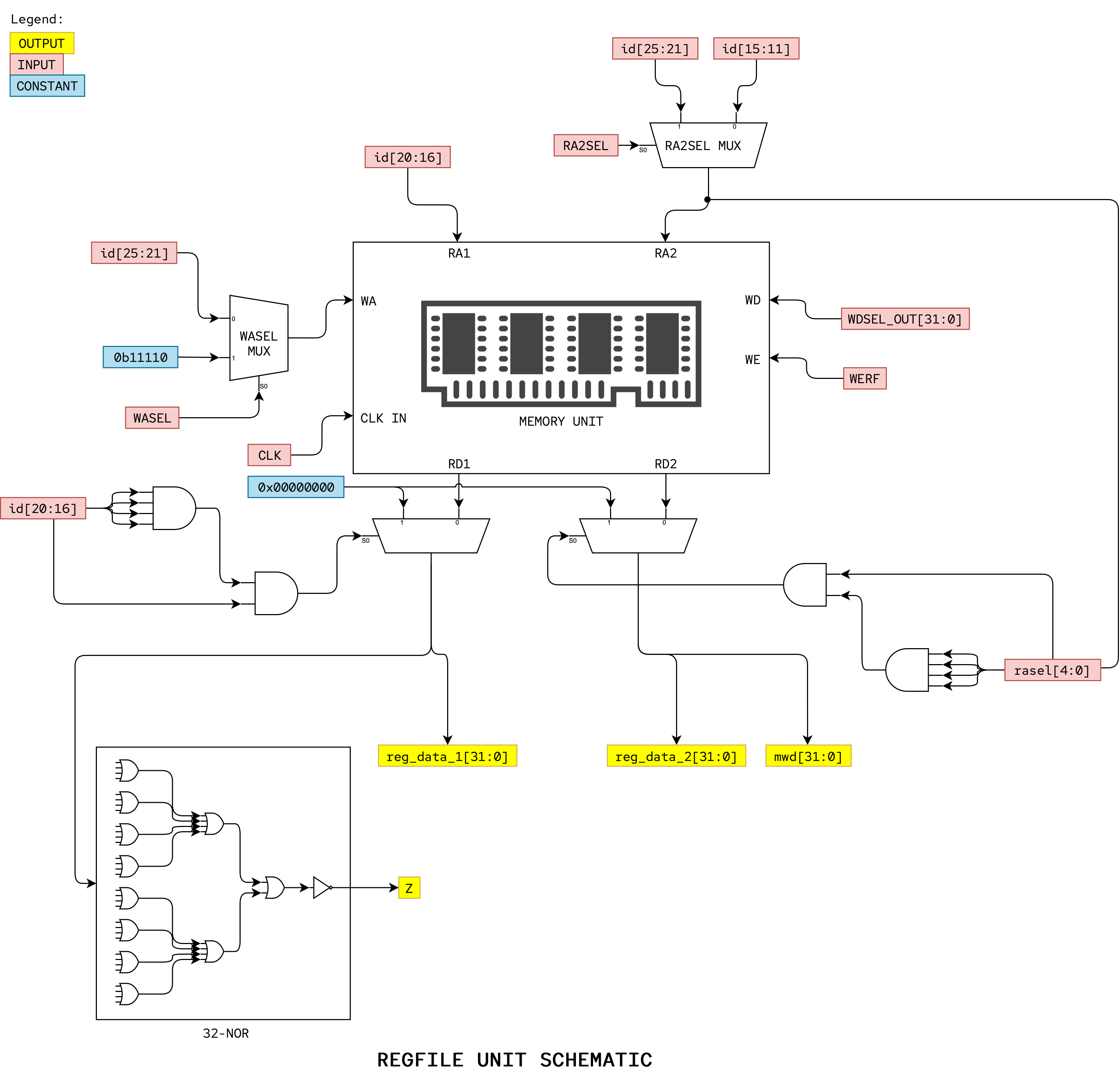
Open regfile_unit.luc and observe that the module interface has been provided for you. We follow the Regfile Unit Schematic above for the declaration of the input and output.
Task 6: RA2SEL and WASEL Mux
You will need a mux controlled by RA2SEL to select the correct address for the B read port. The 5-bit 2-to-1 WASEL multiplexer determines the write address for the register file.
Implement the RA2SEL mux and WASEL mux sections inside regfile_unit.luc.
    // RA2SEL mux
    case(ra2sel){
      // implement the RA2SEL mux logic here
      default:
        ra2sel_out = rb; // default case to silence warnings
    }

    // WASEL mux
    case(wasel){
      // implement the WASEL mux logic here
      default:
        wasel_out = rc; // default case to silence warnings
    }
Task 7: Regfile Memory
The register file is a 3-port memory. It should be implemented in regfile_memory.luc, which is then utilised by regfile_unit.luc.
Implement the workings of the REFGILE unit inside the always block in regfile_memory.luc.
    // implement two output read ports

    // implement one write port
    // check if(write_en) and that we are not writing to R31

    // always give out 0 if we are reading R31 (from either RA ports)
The RD1 port output producing reg_data_1[31:0] is also wired directly as the third (for JMP) input of the PCSEL multiplexer. Remember we already force the low-order two bits to zero and to add supervisor bit logic to bit 31 in the PCSEL Unit, so we do not have to do it here anymore.
Task 8: Z Logic
Z logic can be added to the output of the RA1/RD1 port of the register file memory above. The value of Z must be 1 if and only if reg_data_1[31:0] is 0x00000000. Z must be 0 otherwise. This is exactly a NOR logic. You can create a reduction NOR logic gate very easily in Lucid (well, actually Verilog), but of course you’re welcome to follow the schematic above.
Implement the commpute Z section inside regfile_unit.luc. You can use reduction NOR for this.
Task 9: mwd[31:0] Output
Finally, we need to connect the output of the RD2 port of the register file memory above to produce mwd[31:0].
Implement Task 9 section inside regfile_unit.luc that connects mwd with regfile.reg_data_2.
Part C: CONTROL Unit
CONTROL Unit Schematic
Here is the suggested CONTROL Unit schematic that you can implement.
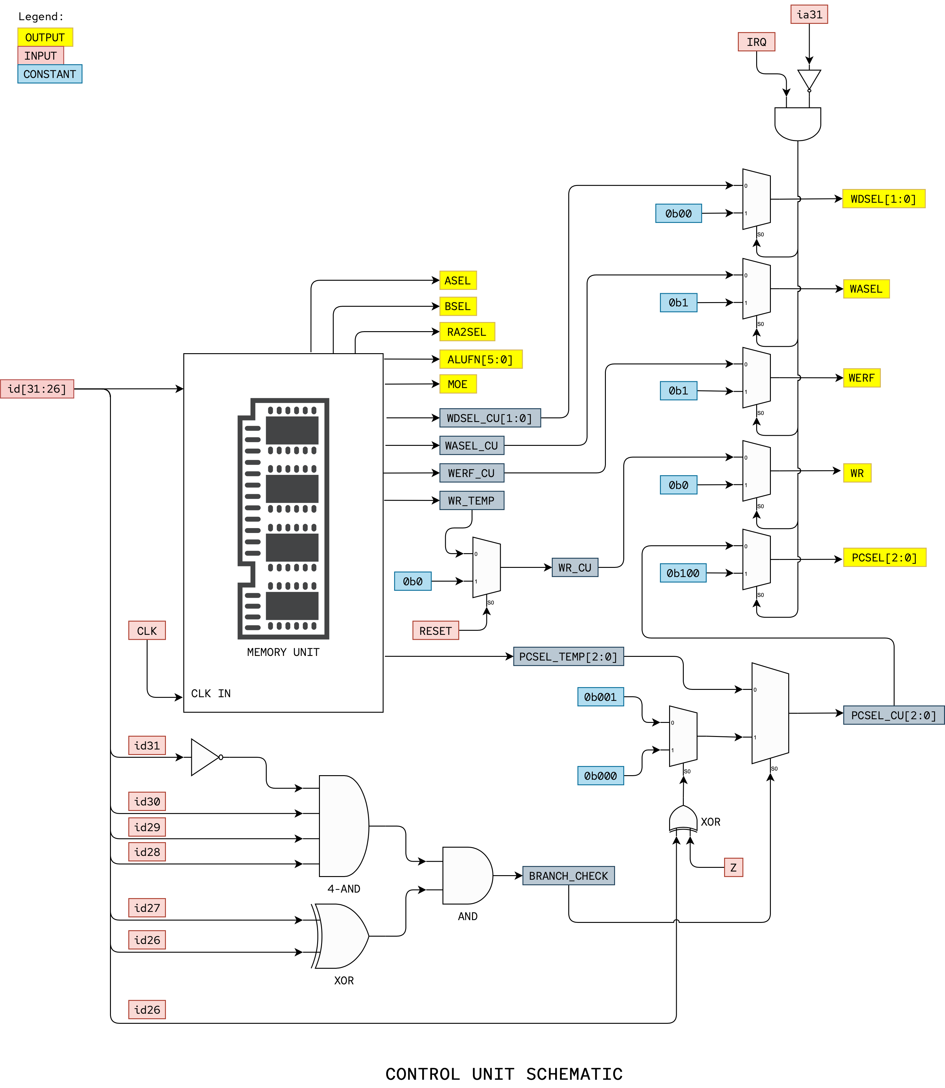
Open control_unit.luc and observe that the module interface has been provided for you. We follow the Control Unit Schematic above for the declaration of the input and output.
ROM
The control logic should be tailored to generate the control signals your logic requires, which may differ from what’s shown in the diagram above. Note that a ROM can be built by simply declaring a CONST array in Lucid.
  const CU_ROM = {
    b01110000000000010,
    b00000011000110110,
    b00000011000010110,
    b00000011000000110,
    b01110000000000010,
    b00000010101100110,
    b00000010111100110,
    b00000010110000110,
    b01110000000000010,
    b00000011101110110,
    ...
Some of the signals can connect directly to the appropriate logic, e.g., ALUFN[5:0] can connect directly to the ALUFN inputs of your ALU, however some signals like PCSEL[2:0] requires some degree of post-processing depending on the value of other signals like Z.
We have already provided you with the bare Control Unit ROM as shown in the schematic above. It gives out control signals, excluding the optional opcodes:
If you need to implement MUL or DIV in your Beta CPU for your 1D, please modify the ROM yourself.
For this lab, further processing for control signals: PCSEL, wasel, wdsel, werf, wr are needed, let’s do this.
WR and WERF
We do need to be careful with the write enable signal for main memory (WR) which needs to be valid even before the first instruction is fetched from memory. WR is an input to the main memory, and recall that ALL inputs need to be VALID (0 is also a valid value!) in order for the main memory to give a valid output data. You should include some additional logic that forces wr to b0 when reset is 1. This takes highest priority, hence it is written at the bottom of the always block in control_unit.luc.
Task 10: PCSEL
The PCSEL logic should take into account the presence of branching BNE/BEQ OPCODE, and output the correct signal depending on the value of Z if branching is indeed happening. Here’s the related OPCODE and PCSEL value:
| OPCODE | Z | PCSEL |
|---|---|---|
BEQ 011101 |
0 | 000 |
BEQ 011101 |
1 | 001 |
BNE 011110 |
0 | 001 |
BNE 011110 |
1 | 000 |
If you are using purely a ROM-based implementation without additional logic (128 words in the ROM as opposed to just 64), you can make Z an additional address input to the ROM (doubling its size). A more economical implementation might use external logic to modify the value of the PCSEL signals as defined in our schematic above.
Complete the PCSEL for BNE/BEQ section inside control_unit.luc.
    // Check of OPCODE == BEQ, and branch (PCSEL: 001) if z == 1
    // Check of OPCODE == BNE, and branch (PCSEL: 001) if z != 1
Task 11: IRQ Handling
When IRQ signal is 1 and the Beta is in “user mode” (PC31 is zero), an interrupt should occur. Asserting IRQ should have NO effect when in “supervisor mode” (PC31 is one). You should add logic that causes the Beta to abort the current instruction and save the current PC+4 in register XP (11110) and to set the PC to 0x80000008. In other words, an interrupt forces the following:
- PCSEL to
b100(select0x80000008as the nextPCvalue) - WASEL to
b1(selectXPas the register file write address) - WERF to
b1(write into the register file) - WDSEL to
b00(selectPC+4as the data to be written into the register file) - WR to
b0(this ensures that if the interrupted instruction was aSTthat it doesn’t get to write into main memory).
Note that you’ll also want to add logic to reset the Beta; at the very least when reset is asserted you’ll need to force the PC to 0x80000000 and ensure that WR is 0 (to prevent your initialized main memory from being overwritten).
Implement IRQ handling section inside control_unit.luc.
    if (irq_sampler.q & slowclk & ~ia31){
      // set all appropriate control signals
      // don't forget to clear the content of irq_sampler dff
    }
Note that the snippet above is located near the end of the always block because it shall overwrite the current instructions’ control signals defined earlier above.
ALU + WDSEL Unit
This unit is fairly straightforward to implement. In fact, it is so easy and we just implement it for you inside beta_cpu.luc.
ALU+WDSEL Unit Schematic
Here is the suggested ALU + WDSEL Unit schematic that we implemented:
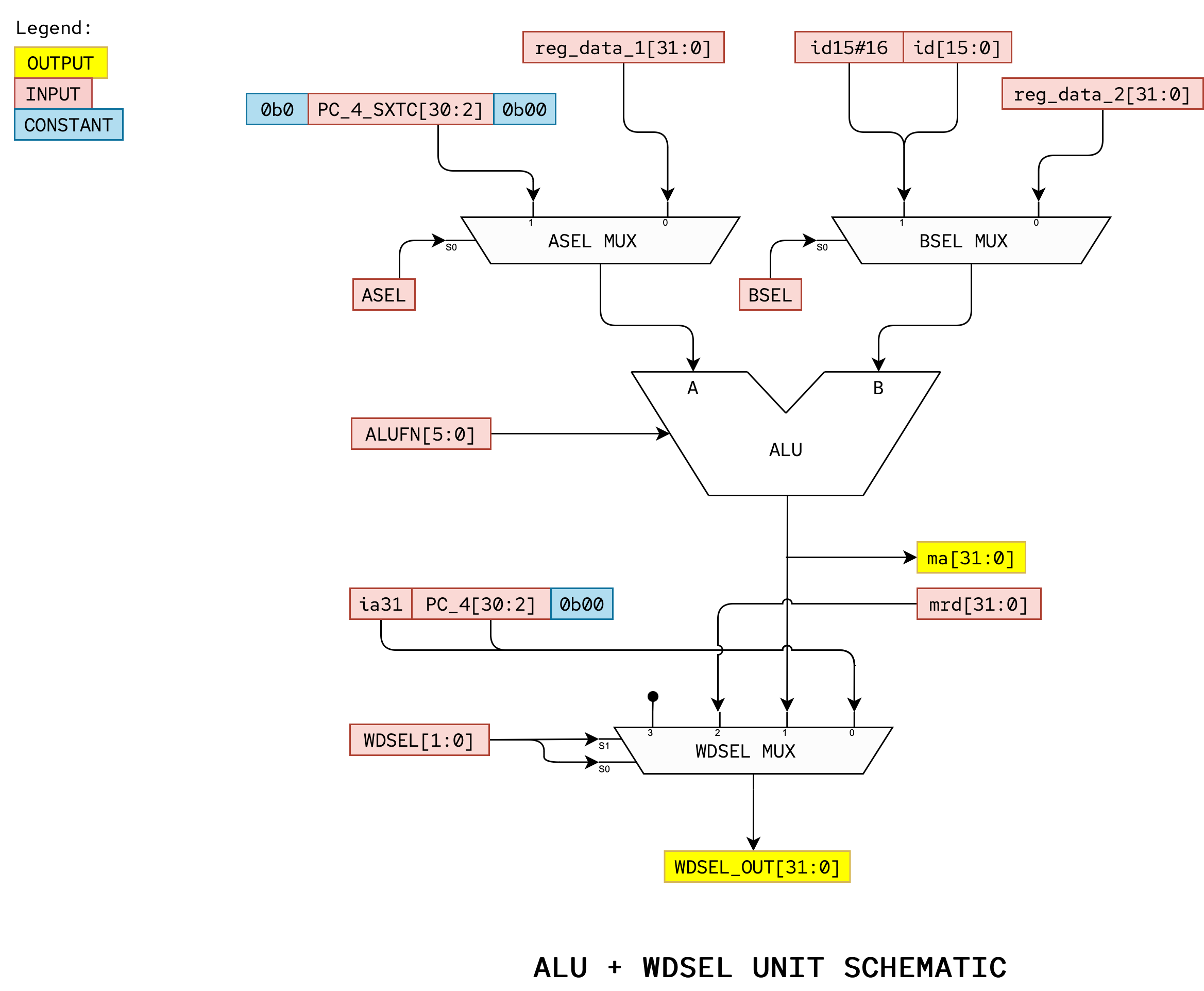
ASEL and BSEL Mux
The low-order 16 bits of the instruction need to be sign-extended to 32 bits as an input to the BSEL mux. Sign-extension is easy in hardware, no extra components needed as you have known already when creating the shift + add component in PC Unit.
Also, Bit 31 of the branch-offset input to the ASEL mux should be set to 0. This means that the supervisor bit is ignored when doing address arithmetic for the LDR instruction.
WDSEL Mux
Bit 31 of the PC+4 input to the WDSEL mux should connect to the highest bit of the PC Reg output, ia31, saving the current value of the supervisor whenever the value of the PC is saved by a branch instruction or trap. This is already handled in the PC unit. You don’t need to do anything else here.
Part D: Assemble Completed Beta
Task 12
The complete schematic of the Beta is (you might want to open this image in another tab):
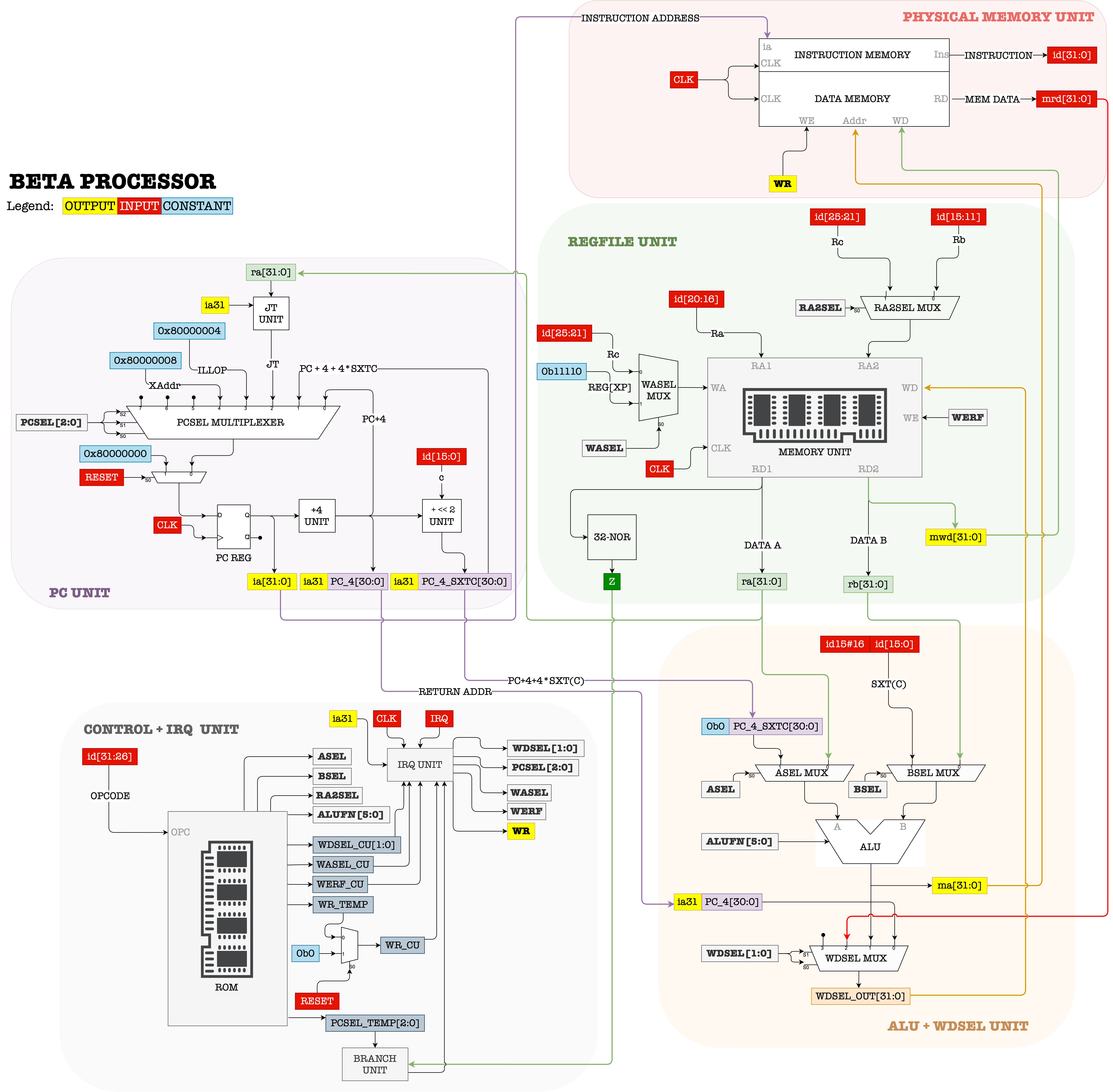
Open beta_cpu.luc and study the starter code. The 4 major components of the Beta has been instantiated for you.
  control_unit control_system(.clk(clk), .rst(rst));
  alu alu_system;
  regfile_unit regfile_system(.clk(clk), .rst(rst));
  pc_unit pc_system(.clk(clk));
Complete Task 12 section that defines connections to the control unit, PC unit, and regfile unit respectively.
    //***** CONTROL unit ******//
    // connect all input terminals of Control Unit to IRQ, pc_system, instruction, regfile_system, and slowclk accordingly

    //***** PC unit ******//
    // connect all input terminals of pc_system to slowclk, REGFILE, Control System, and instruction
    // connect ia to pc_system.ia so we can use that for other parts of the datapath


    //***** REGFILE unit *****//
    // connect all regfile input ports accordingly, all read addresses and write addresses, as well as slowclk, and control signals
Finally, we need our beta to produce appropriate output signals. Complete theoutput connections section in beta_cpu.luc.
    // connect alu_system with asel_out and bsel_out
    // connect regfile_system with wdsel_out
    // connect signals mem_data_address with the output of the ----------
    // connect mem_data_output with regfile_system
    // finally, connect wr sig with control_system
Connect Debug Signals
It is really hard to debug your FPGA and it takes a long time to compile your Lucid code. As such, it always helps to create additional debug output so that we can “inspect” the content of each crucial component in the Beta CPU during each instruction execution.
Paste the debug code below under debug signals section in beta_cpu.luc.
    debug[0][15:0] = pc_system.pc_4_sxtc[15:0];
    debug[1][15:0] = asel_out[15:0];
    debug[2][15:0] = bsel_out[15:0];
    debug[3][15:0] = wdsel_out[15:0];
You may change it to suit your use case if you wish.
Compile and Run
Congratulations! 🎉
You have made a working Beta CPU. Please take your time to understand how each component works. You shall now compile, run the program and then vary io_dip[0] switches to inspect each state. In au_top.luc, we have linked up the io_led[1:0] to various debug signals.
io_dip[0] can be changed to “view” various states presented at io_led[1] and io_led[0] (16 bits of values at once). Simply set it to represent the values below, e.g: 0x3 means that io_dip[0] is set to 00000011 (turn the rightmost two switches on). Here is the exhaustive list:
0x0: MSB 16 bits of current instruction (id[31:16])0x1: LSB 16 bits of current instruction (id[15:0])0x2: LSB 16 bits of instruction address (ia[15:0])0x3: LSB 16 bits of EA (this is also ALU output) (ma[15:0])0x4: MSB 16 bits of EA (this is also ALU output) (ma[31:16])0x5: LSB 16 bits of Mem[EA] (mrd[15:0])0x6: MSB 16 bits of Mem[EA] (mrd[31:16])0x7: LSB 16 bits of RD2 (mwd[15:0])0x8: MSB 16 bits of RD2 (mwd[31:16])0x9: LSB 16 bits of pcsel_out0xA: LSB 16 bits of asel_out0xB: LSB 16 bits of bsel_out0xC: LSB 16 bits of wdsel_out0xD: MSB 16 bits of instruction address. Useful to see PC31 (kernel/user mode) (ia[31:16])0xE: LSB 16 bits of beta input buffer. This is a dff that’s hardwired to reflect Mem[0x10]0xF: LSB 16 bits of beta output buffer. This is a dff that’s hardwired to reflect Mem[0xC]
We have also provided all this information in the repository’s readme.
Observed Output
Initial State
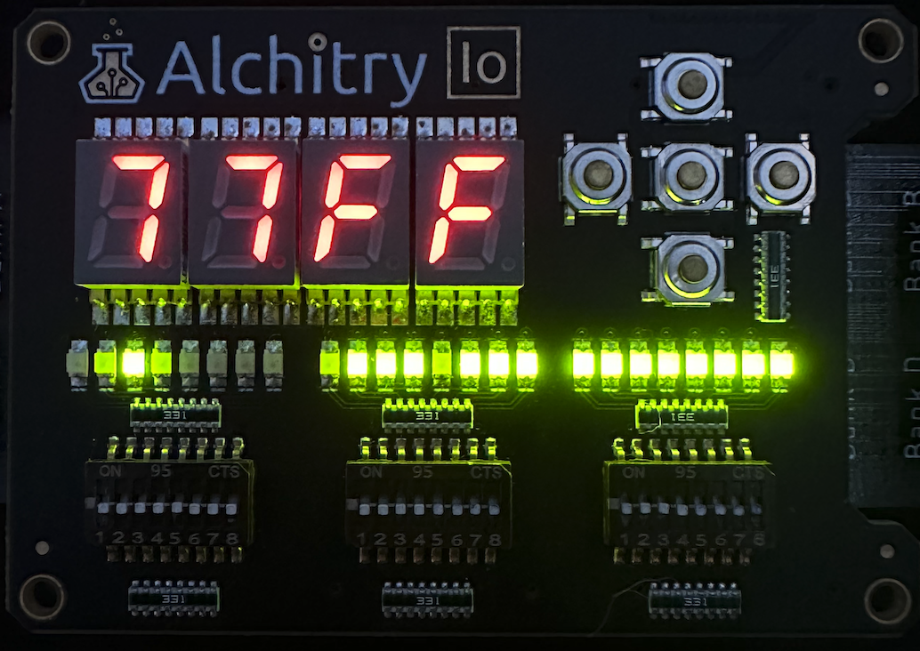
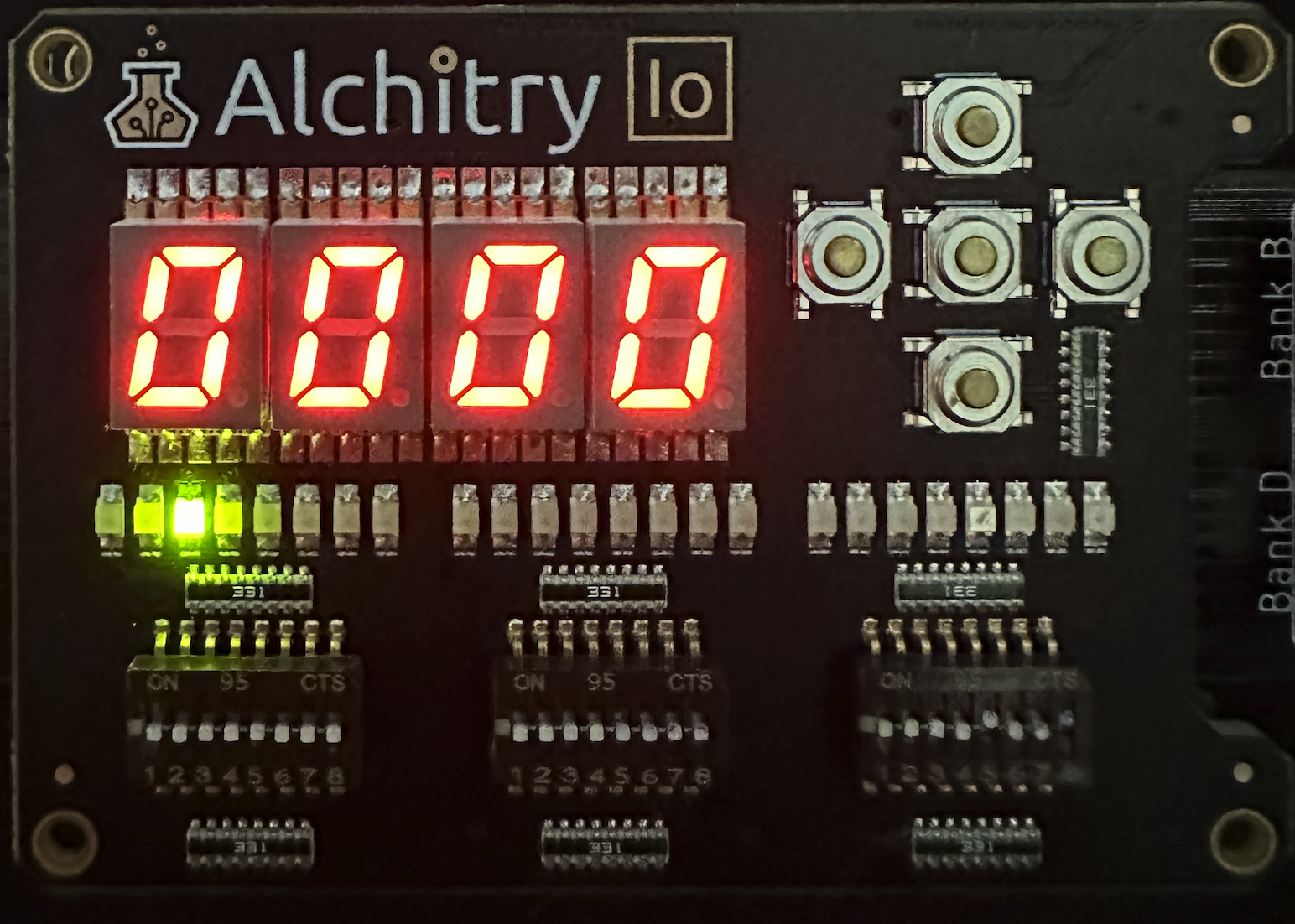
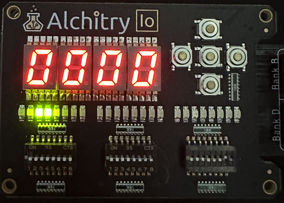
Upon flash to the FPGA, with ALL switches down, you should see the following.
io_led[1:0] is showing MSB 16 bits of current instruction (id[31:16]) which is BEQ(R31, 0, R31): 0x77FFFFFF.
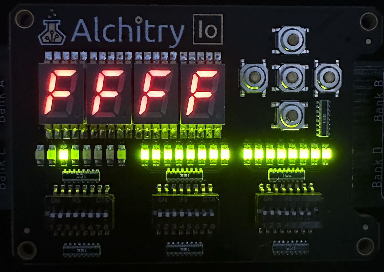
io_dip[0] to 0x01
Then, set io_dip[0] to 0x01 (rightmost switch up). You shall see the LSB 16 bits of current instruction.
io_dip[0] to 0x02
Confirm that the current PC is pointing at address 0x80000000. Observe its last 16 bits value:
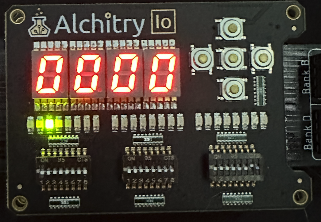
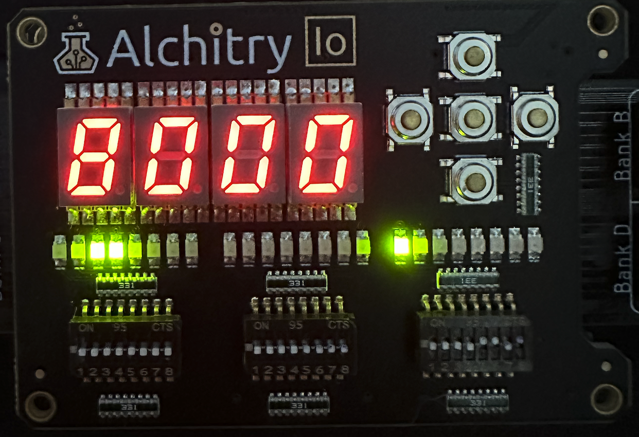
io_dip[0] to 0x0D
Then, observe PC first 16 bits value:
Kernel Address Space
Note that PC is set to
0x80000000instead of0x00000000because uponreset, we shall technically execute the reset handler, which part of the Kernel program that “prepares” your machine upon start up. A kernel program must be placed in the Kernel address space (address space with MSB of1) instead of user address space.
io_dip[0] to 0x9
Finally, observe that the last 16 bits of pcsel_out (the next PC value) still points to 0 (as per the instruction).
A Better Test Instruction
Now we need to test it by giving it a simple starter code (well, should’ve tested each and every component up above, but we don’t have enough time in class).
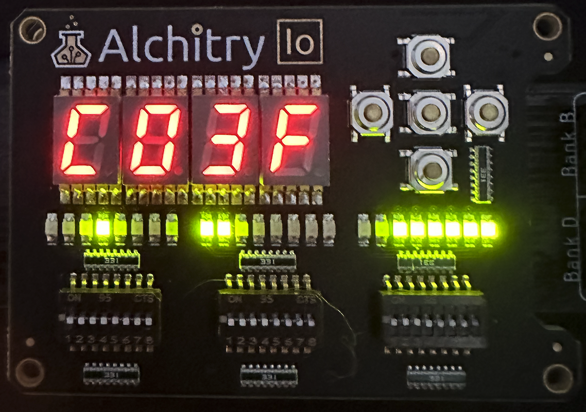
Paste the following simple driver code inside instruction_rom.luc, under const INSTRUCTIONS, replacing the existing instruction. You will need this for your Checkoff for this lab (due lab time, Week 10).
    32h7BE3FFFB, // 0x010 BNE(R3, main, R31)
    32h607F0020, // 0x00C LD(R31, 32, R3)
    32h643F0020, // 0x008 ST(R1, 32, R31)
    32h90410800, // 0x004 CMPEQ(R1, R1, R2)
    32hC03F0003 // 0x000 ADDC(R31, 3, R1) --- main
Compile, and run the Beta FPGA again while observing that the states: id, ia, pcsel_out, etc should match the truth.
What is the true value for all these states? Well, you learned the Beta ISA in the first half of the semester, didn’t you? You should know how it works.
You can also paste this equivalent program in bsim and observe its states, ensure that it matches the FPGA’s (yes, manual observation).
.include beta.uasm

ADDC(R31, 3, R1)
CMPEQ(R1, R1, R2)
ST(R1, 32, R31)
LD(R31, 32, R3)
BNE(R3, 0, R31)
Observed Output
Ensure to put all switches down at first.
Upon compilation and flashing of the new 5-line instructions for the first time, we are met with a new instruction ADDC(R31, 3, R1): 0xC03F0003.
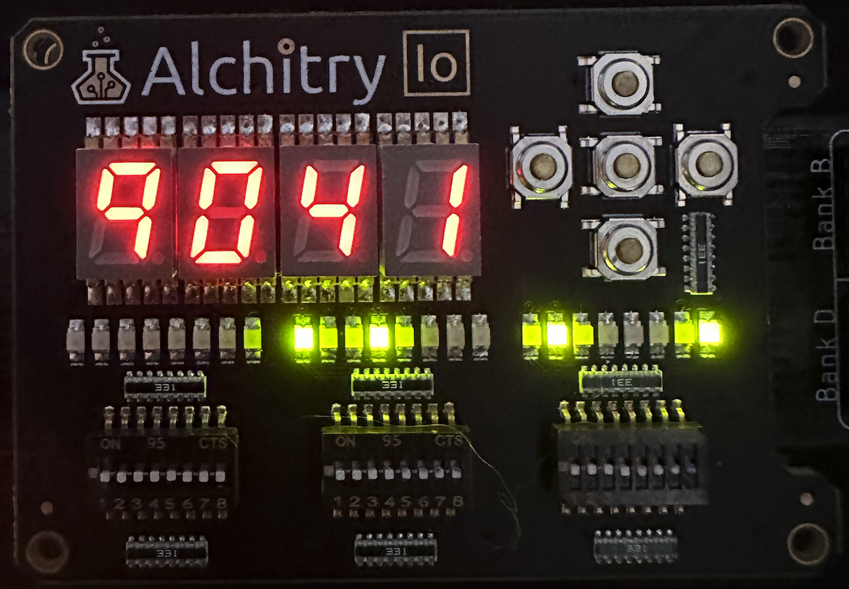
To advance to the next instruction, press the RIGHT io button (io_button[4]). You shall see the first 16 bits of the second instruction (CMPEQ) now:
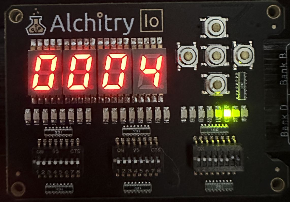
Set io_dip[0]: 0x02 to confirm that you’re indeed pointing at address 4:
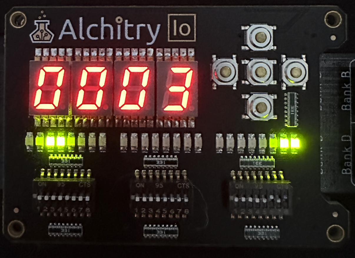
Press RIGHT io button once again to advance until the third instruction (ST) at address 0x8. At this point, we are about to store the content of R1 to the memory device.
You can confirm that this value is indeed 3 in the next instruction (LD, press RIGHT io button one more time), by setting your io_dip[0]: 0x5 to view mrd[15:0]:
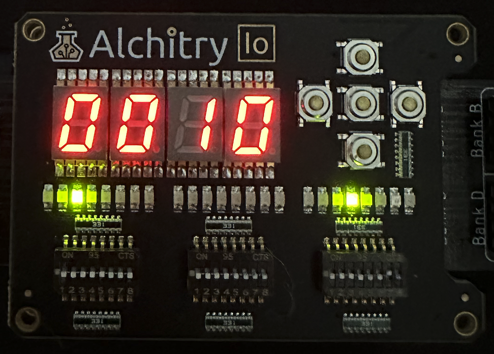
Finally, when you reach the fifth instruction at address 0x10 (BNE), confirm that you will loop back to execute the first instruction at address 0x0. Don’t forget to set your io_dip[0]: 0x02 to view ia[15:0].
Before:
After:
Checkoff
As stated in the beginning of this document, you need to complete all the above tasks and demonstrate a working Beta CPU using the “better test instructions” above by the end of next week’s lab. You can checkoff as a group. Only group members who are present gain the marks (unless valid LOA).
Checkoff
You need to demonstrate that your FPGA works as the above with the test instruction to your TA/instructor by the end of next week’s lab (during lab hour).
What’s Next?
In the next lab, we will study more on how motherboard.luc works and drive the Beta CPU, and how to handle special events like irq, illop, and reset properly. We will connect I/O to interact with our Beta, kinda like connecting a keyboard and a screen to our computer (but a way simplied version of it).