- TOC
50.002 Computation Structures
Information Systems Technology and Design
Singapore University of Technology and Design
Modified by: Kenny Choo, Natalie Agus, Oka Kurniawan (2021)
Lab 4: Beta Processor
Starter Code
The following files inside your /50002/ folder are what you’re going to open and modify or study for this lab, then submit (unless otherwise stated):
lab4_pc.jsimlab4_regfile.jsimlab4_control.jsimlab4_aluwdsel.jsim(for study only, no submission of this file is required)lab4_beta.jsim
Related Class Materials
The lecture notes on Building the Beta CPU, and Designing an Instruction Set are closely related to this lab.
This lab will reinforce your understanding on how the Beta CPU works, and all data paths for OP, OPC, Control Transfer, and Memory Access operations.
Related sections in Designing an Instruction Set:
- The Von Neumann model: CPU, Memory, IO
- Programmability of a Von Neumann Machine: basics of programmable control systems (using control signals like
OPCODEto activate different data paths in the Beta CPU). - Beta ISA Format
- Beta Instruction Encoding
Related sections in Beta CPU:
- OP datapath
- OPC datapath
- Memory Access datapath
- This lab will help you to familiarise yourselves with all Beta instructions
- Control transfer datapath
- Exception handling
- By the end of this lab, you should know how to build the schematic of the entire Beta CPU based on its ISA (blueprint)
Introduction
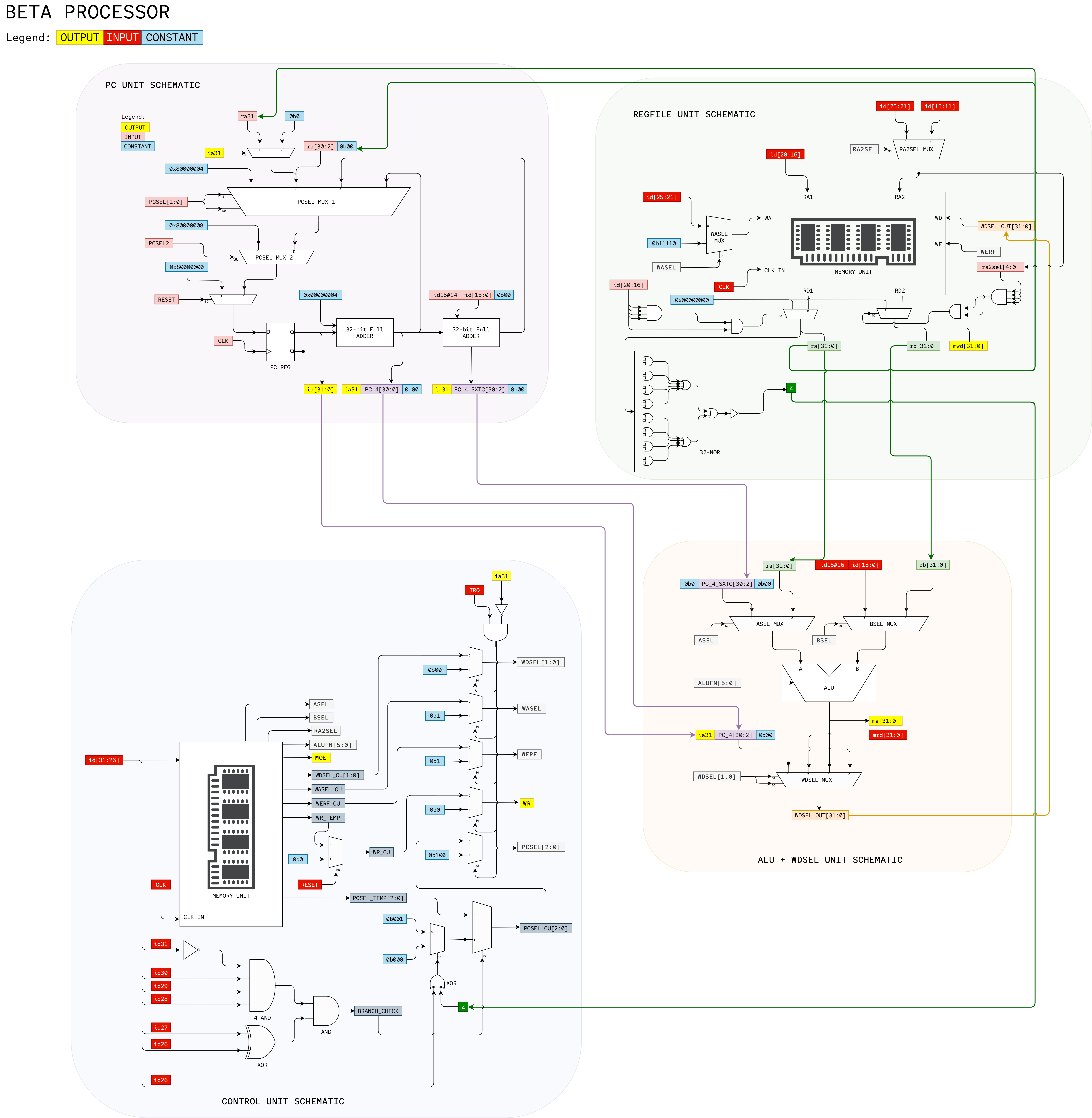
The goal of this lab is to build a fully functional Beta Processor. It is a huge device, and to make it more bearable we shall modularise it into four major components:
- (Task A) PC Unit: containing the PC register and all necessary components to support the ISA
- (Task B) REGFILE Unit: containing 32 32-bit registers, WASEL, and RA2SEL mux, plus circuitry to compute Z
- (Task C) CONTROL Unit: containing the ROM and necessary components to produce all Beta control signals given an
OPCODE - ALU+WDSEL Unit: containing the ALU and WDSEL, ASEL, BSEL muxes (given to you)
- (Task D) Assemble the entire Beta CPU using all subcomponents above
The signals indicated in red refers to external INPUT to our Beta, supplied by the Memory Unit defined in our checkoff file:lab4checkoff.jsim. The signals indicated in yellow refers to our Beta’s OUTPUT to the Memory Unit defined in lab4checkoff.jsim.
Bus unit
There exist the bus unit inside stdcell.jsim that will come in handy to duplicate certain nodes for you with a different name. It is defined as such:
1
2
3
.subckt bus a b
.connect a b
.ends
Therefore if you want to duplicate node a[31:0] into node b[31:0], simply state (position of a and b can be interchangeable, it does not matter):
1
Xbusab a[31:0] b[31:0] bus
Then you can utilise node b[31:0] afterwards.
Memory Unit
The Memory Unit is broken into two sections for clarity:
- the instruction memory and
- the data memory
The schematic of the memory unit is as follows:
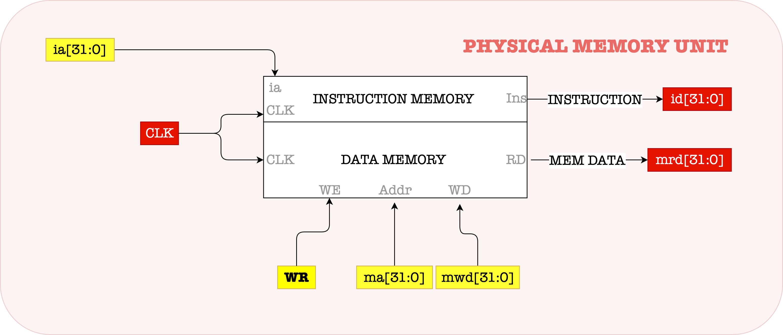
These two will be supplied by lab4checkoff.jsim, a file inside 50002; you just need to set the Beta to supply the appropriate signals to each unit.
Instruction Memory
The input to the instruction memory supplied by the Beta is: instruction address (ia[31:0]). This contains the address of the next instruction to be executed.
This will cause the instruction memory to output the following for the Beta CPU: instruction data (id[31:0]) from lab4checkoff.jsim.
Note: After the appropriate propagation delay, the memory unit will supply the Beta with the contents of its memory location specified by
ia[31:0].
Data Memory
The Beta CPU can read or write to the Data Memory.
Read
The Data Memory Unit receives two input from the Beta:
- data memory address (
ma[31:0]). This is the address of data memory location where we want to read (load) from or write (store) to. - memory output enable (
moe). This is set to1when the Beta wants the memory to fetch the data at the memory location specified byma[31:0]. Otherwise it is set to0, causingma[31:0]to be0x00000000.
When the Beta wants to load (read) data from the memory, it needs to supply the above two things to the memory unit. Supplying the two things above will cause the data memory to output the following for the Beta CPU: memory read data (mrd[31:0]).
Write
If the Beta wants to store (write) data to the memory, it needs to supply two signals to the data memory:
- memory write data (
mwd[31:0]) – the 32-bit data to be stored to the memory unit, and, - memory write enable (
wr). Set to 1 when the Beta wants to store into the memory location specified byma[31:0]at the end of the current cycle.
Task A: PC Unit
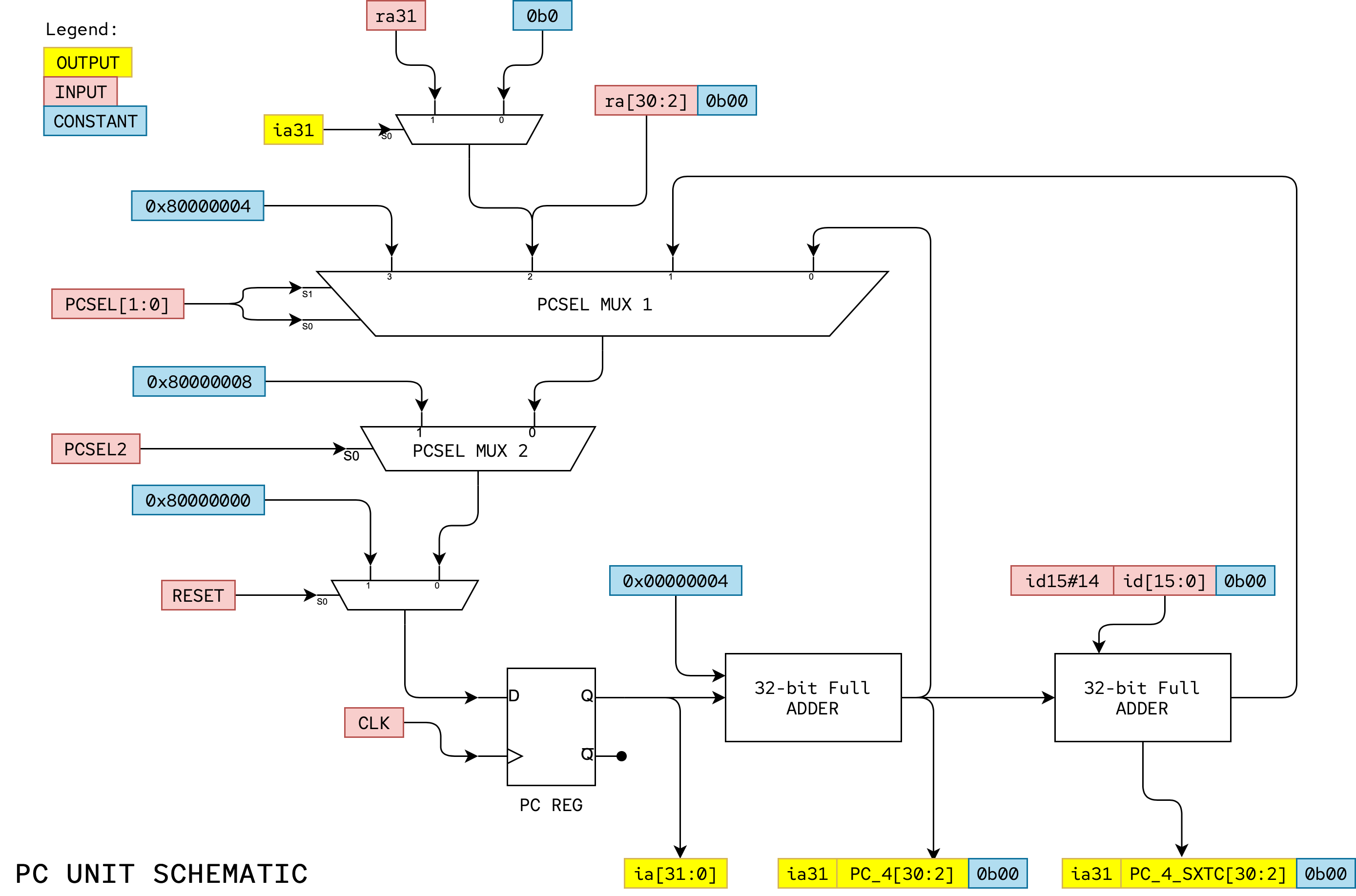
PC Unit Schematic
Here is the suggested PC Unit schematic that you can implement. Note the input and output nodes. This will come in very useful when creating the modules for your jsim subckt.
Open lab4_pc.jsim and observe that the module interface has been provided for you. We follow the PC Unit Schematic above for the declaration of the input and output (they are positional arguments):
1
2
3
.subckt PC_UNIT clk reset id[15:0] PCSEL[2:0] ra[31:0] ia[31:0] PC_4_SXTC[31:0] PC_4[31:0]
...
.ends
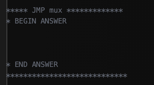
Your job is to fill up each blanks between BEGIN ANSWER and END ANSWER
PCSEL Multiplexers
The 32-bit 5-to-1 PC multiplexer (mux) selects the value to be loaded into the PC at the next rising edge of the clock depending on the PCSEL control signal.
Since the parts library doesn’t have any 5-input multiplexers, you will have to construct the logic that selects the next PC using other components (mux2 and mux4) and adjust the control logic accordingly (see schematic above).
In short, here’s the declaration:
1
Xid S0 S1 d0 d1 d2 d3 z mux4
And it means as follows:
| S0 | S1 | z |
|---|---|---|
| 0 | 0 | d0 |
| 1 | 0 | d1 |
| 0 | 1 | d2 |
| 1 | 1 | d3 |
Hence the order of S0 and S1 matters very much.
XAdr and ILLOP in the Beta diagram in our lecture notes represents constant addresses used when the Beta services an interrupt (triggered by IRQ) or executes an instruction with an illegal or unimplemented opcode. For this assignment assume that XAdr=8 and ILLOP=4 and we will make sure the first three locations of main memory contain BR instructions that branch to code which handle reset, illegal instruction traps and interrupts respectively. In other words, the first three locations of main memory contain:
1
2
3
Mem[0x80000000] = BR(reset_handler)
Mem[0x80000004] = BR(illop_handler)
Mem[0x80000008] = BR(interrupt_handler)
We have given you the nodes for constant 0x80000008 and 0x80000004 called XAddr[31:0] and ILLOP[31:0], please utilise that.
You also have to force the lower two bits of inputs going into the PC+4, PC+4+4*SXTC, and JT port of the mux to be 0b00. You can do this with appropriate wiring.
Example:
1
Xmux_unit control_signal#32 input_signal_a[31:2] 0#2 input_signal_b[31:2] 0#2 output_signal[31:0] mux2
- In the example above, we create 32 bit 2-to-1 multiplexers, so we have to duplicate the
control_signal32 times - Instead of using all 32 bits of
input_signal_a[31:0], we can just use the upper 30 bits, and append the lower two bits with two zeros using0#2. - The same is done for the second input signal to the mux:
input_signal_b[31:2] 0#2 - JSim will automatically segment each signals to create 32 2-to-1 muxes. It is equivalent to writing:
1
2
3
4
5
6
Xmux_unit31 control_signal input_signal_a31 input_signal_b31 output_signal31 mux2
Xmux_unit30 control_signal input_signal_a30 input_signal_b30 output_signal30 mux2
...
Xmux_unit2 control_signal input_signal_a2 input_signal_b2 output_signal2 mux2
Xmux_unit1 control_signal 0 0 output_signal1 mux2
Xmux_unit0 control_signal 0 0 output_signal0 mux2
RESET Multiplexer
Remember we need to add a way to set the PC to zero on reset. We use a two-input 32-bit mux that selects 0x80000000 when the RESET signal is asserted, and the output of the PCSEL mux when RESET is not asserted. We will use the RESET signal to force the PC to zero during the first clock period of the simulation.
We have given you the nodes for constant 0x80000000 called RESET[31:0], please utilise that.
32-bit PC Reg
The PC is a separate 32-bit register that can be built using the dreg component from the standard cell library, see Appendix.
You should include hardware for the bottom two bits of the PC even though they are always 0 anyway in this simulation; this will make debugging traces easier to interpret.
Increment-by-4
Conceptually, the increment-by-4 circuit is just a 32-bit adder with one input wired to the constant 4. You can reuse the 32-bit FA circuit that you have created in Lab 3. However, it is possible to build a much smaller circuit if you design an adder optimized knowing that one of its inputs is 0x00000004 constant.
We have given you the nodes for constant 4 called FOUR[31:0] and implemented the add-4 unit for you as follows in lab4_pc.jsim:
Please study the code as it will help you implement the shift-add-4 unit next.
Shift-and-add
The branch-offset adder adds PC+4 to the 16-bit offset encoded in the instruction id[15:0]. You can use adder32 again here. The offset is sign-extended to 32-bits and multiplied by 4 in preparation for the addition. Both the sign extension and shift operations can be done with appropriate wiring—no gates required!
Supervisor Bit
The high-order bit of the PC is dedicated as the “Supervisor” bit (see section 6.3 of the Beta Documentation). The LDR instruction ignore this bit, treating it as if it were zero. The JMP instruction is allowed to clear the Supervisor bit or leave it unchanged, but cannot set it, and no other instructions may have any effect on it. Only reset, exceptions and interrupts cause the Supervisor bit to become set. This has the following implications for your Beta design:
-
0x80000000,0x80000004and0x80000008are loaded into the PC duringreset,ILLOPandIRQrespectively. This is the only way that the supervisor bit gets set. Note that after reset the Beta starts execution in supervisor mode. -
Bit 31 of the
PC+4and branch-offset inputs to the PCSEL mux should be connected to the highest bit of the PC Reg output,ia31; i.e., the value of the supervisor bit doesn’t change when executing most instructions.- Please ensure your answer in shift-and-add section takes this into account.
- We gave a sample implementation under add-4 unit:
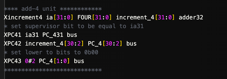
-
You’ll have to add logic to bit 31 of the
JTinput to the PCSEL mux to ensure that JMP instruction can only clear or leave the supervisor bit unchanged. Here’s a table showing the new value of the supervisor bit after aJMPas function of JT31 and the current value of the supervisor bit (PC31):old PC31 (ia31) JT31 (ra31) new PC31 0 – 0 1 0 0 1 1 1
Testing
You can uncomment the headers inside lab4_pc.jsim and run the gate-level simulation:
1
2
3
4
.include "nominal.jsim"
.include "stdcell.jsim"
.include "lab4_adder.jsim"
.include "lab4_testpc.jsim"
You should see the plot window pops up as such:
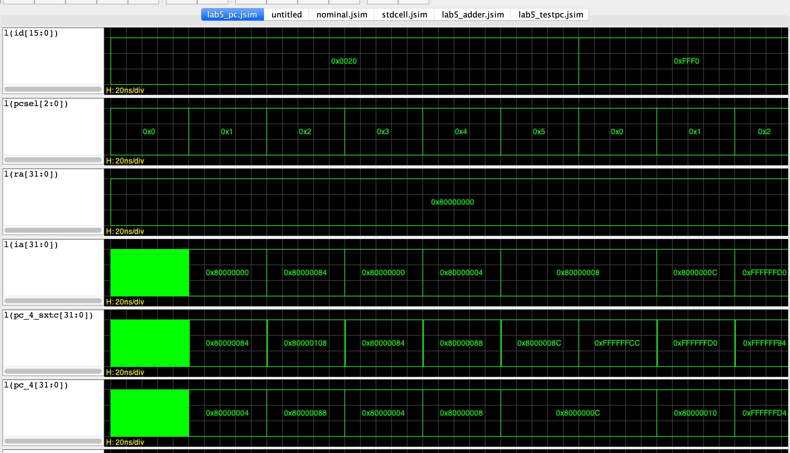
Study the output to ensure that you have the intended signals. You can click on the tick button, and if there’s no error you shall see the following verification window for the pc unit:
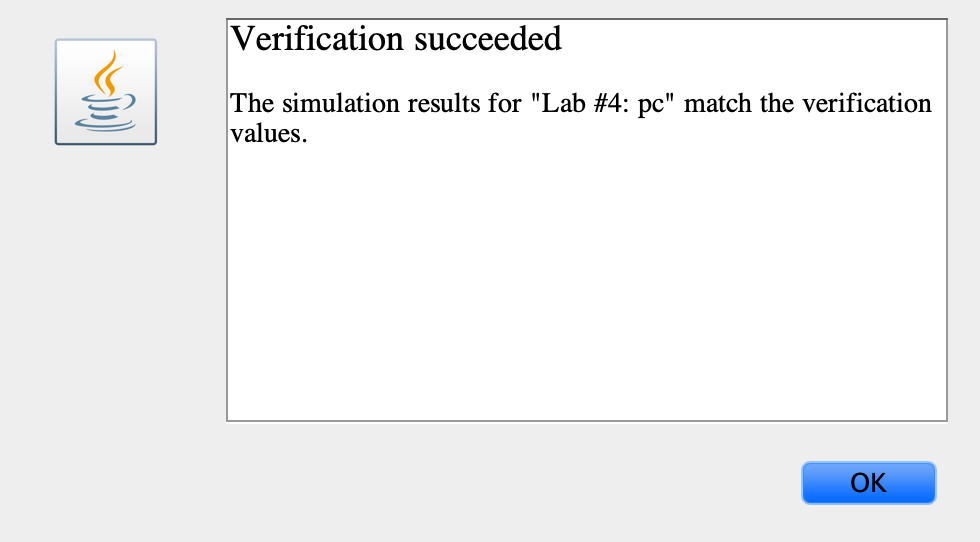
IMPORTANT: comment back the header and the test instructions after you are done. The file lab4_pc.jsim should only contain the definition of your pc unit subcircuit only. We will import it later inside lab4_beta.jsim.
Task B: REGFILE Unit
REGFILE Unit Schematic
Here is the suggested REGFILE Unit schematic that you can implement.
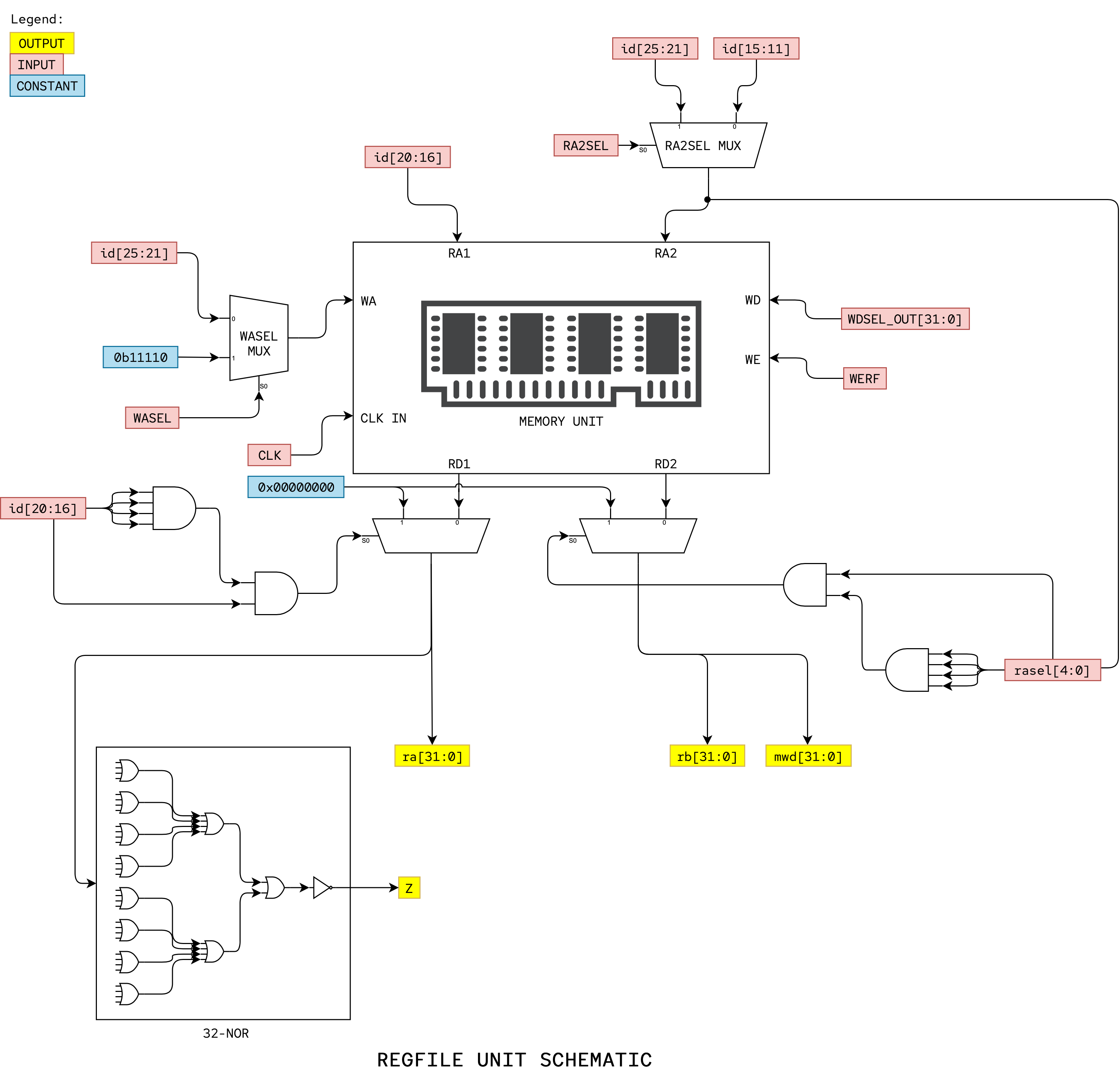
Open lab4_regfile.jsim and observe that the module interface has been provided for you. We follow the Regfile Unit Schematic above for the declaration of the input and output (they are positional arguments):
1
2
3
.subckt REGFILE_UNIT clk wasel ra2sel werf id[25:11] WDSEL_OUT[31:0] ra[31:0] rb[31:0] mwd[31:0] z
...
.ends
Again, your job is to fill up each blanks between BEGIN ANSWER and END ANSWER
WASEL and RA2SEL Mux
You will need a mux controlled by RA2SEL to select the correct address for the B read port. The 5-bit 2-to-1 WASEL multiplexer determines the write address for the register file.
We have provided the address for Reg XP for you, that is the 5-bit constant 30: 0b11110. Please utilise that in your implementation.
Memory
The register file is a 3-port memory. Here’s a template netlist for specifying the 3-port register file using JSim $memory component:
1
2
3
4
5
Xregfile
+ vdd 0 0 ra[4:0] adata[31:0]     // A read port
+ vdd 0 0 ra2mux[4:0] bdata[31:0] // B read port
+ 0 clk werf rc[4:0] wdata[31:0]  // write port
+ $memory width=32 nlocations=31
See Appendix 2 at the end of this handout for a more complete description of how to use the
$memoryJSim component.
Note that the memory component doesn’t know that location 31 of the register file should always read as 0x00000000, so you’ll have to add additional logic around the memory that makes this happen. You can use muxes or ANDs to force the register data for each read port to “0” when the port address = 0b11111 (i.e., R31).
Recall that the RA1/RD1 port output producing
ra[31:0]is also wired directly to theJTinputs of thePCSELmultiplexer (remember we already force the low-order two bits to zero and to add supervisor bit logic to bit 31 in the PCSEL Unit, so we do not have to do it here anymore).
Z Logic
Z logic can be added to the output of the RA1/RD1 port of the register file memory above. The value of Z must be 0b1 if and only if ra[31:0] is 0x00000000. Z must be 0b0 otherwise. This is exactly a NOR logic, but we do not have a 32-bit NOR gate. Hence we can use a fan-in OR gates and place an inverter at the end as shown in the schematic above.
mwd[31:0] Output
Finally, connect the output of the RD2 port of the register file memory above to produce mwd[31:0]. You can use the bus connection provided inside stdcell as explained above. For instance, if the output of the RD2 port of your regfile memory is called rb[31:0], we can create mwd[31:0] as such:
1
Xmwdout mwd[31:0] rb[31:0] bus
Testing
You can uncomment the headers inside lab4_regfile.jsim and run the gate-level simulation to verify that your unit works perfectly:
1
2
3
.include "nominal.jsim"
.include "stdcell.jsim"
.include "lab4_testregfile.jsim"
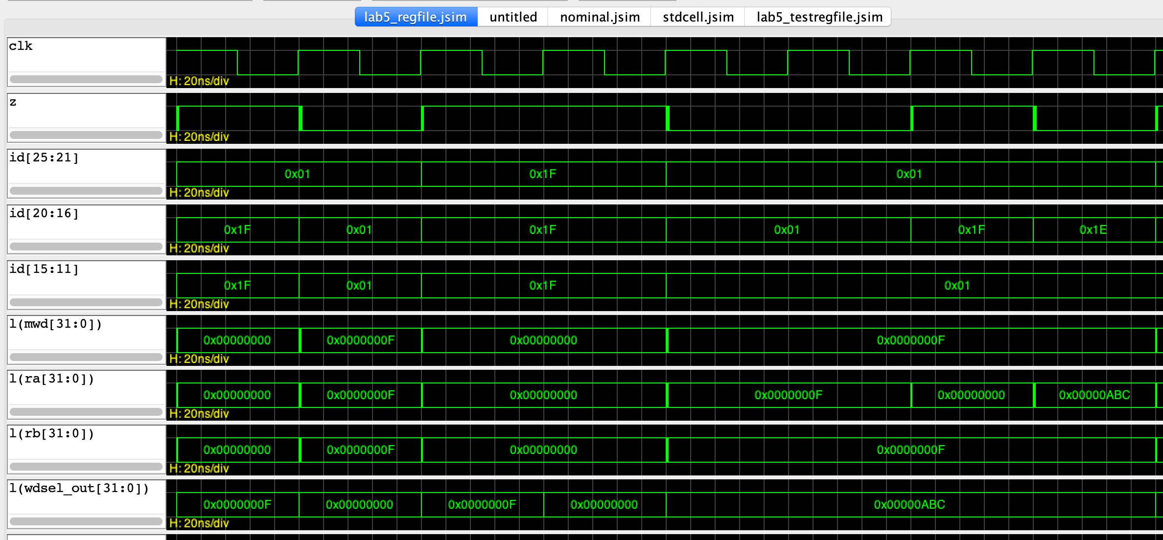
If everything works as expected, you should see the following message when you click the green tick:
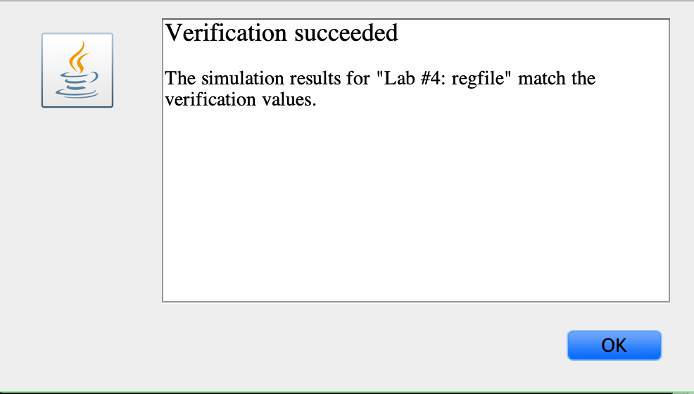
IMPORTANT: comment back the header and the test instructions after you are done. The file lab4_regfile.jsim should only contain the definition of your pc unit subcircuit only. We will import it later inside lab4_beta.jsim.
Task C: CONTROL Unit
CONTROL Unit Schematic
Here is the suggested CONTROL Unit schematic that you can implement.
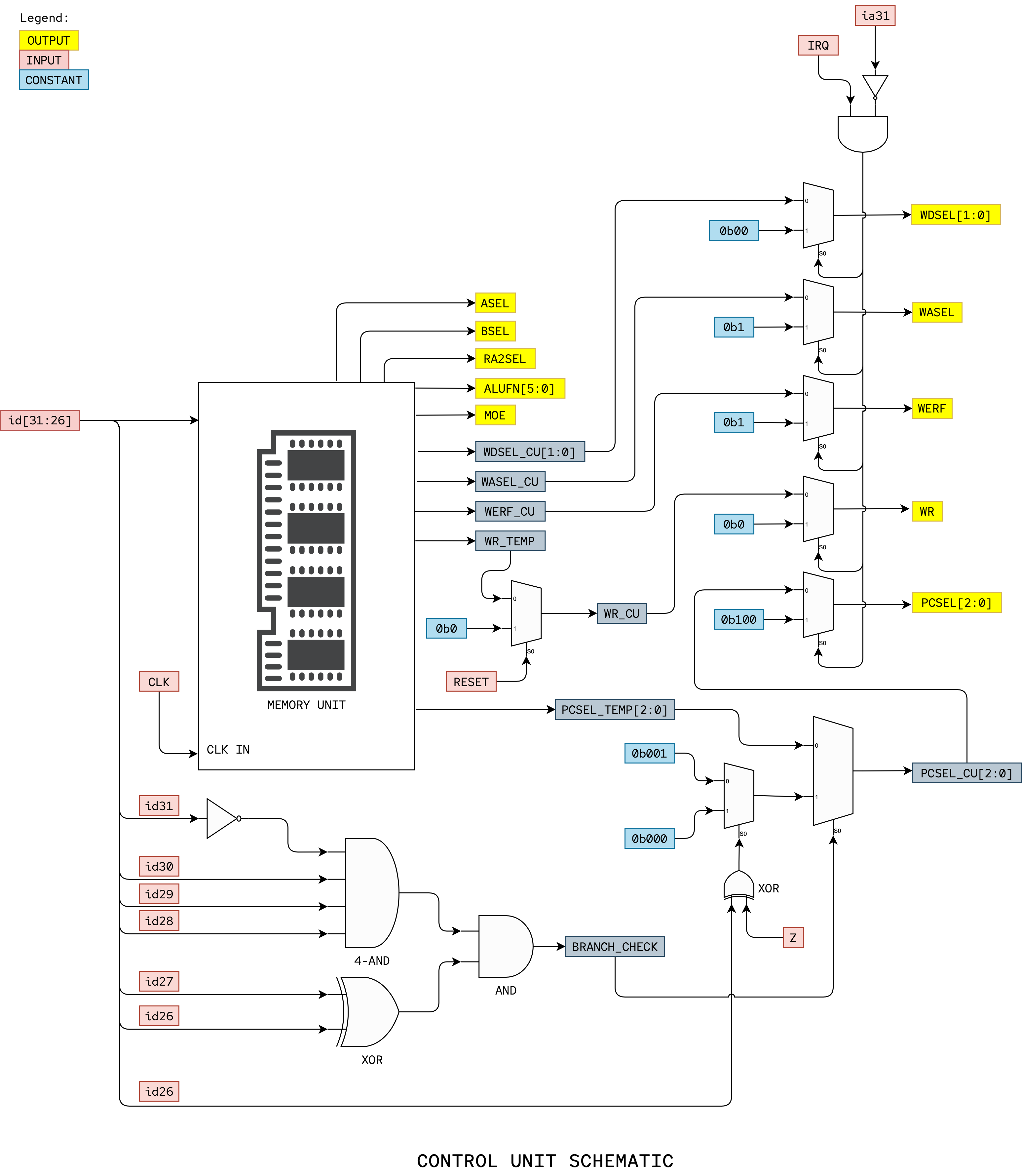
Open lab4_control.jsim and observe that the module interface has been provided for you. We follow the Control Unit Schematic above for the declaration of the input and output (they are positional arguments):
1
2
3
.subckt CONTROL_UNIT z reset irq ia31 id[31:26] asel bsel ra2sel alufn[5:0] moe wdsel[1:0] wasel werf wr pcsel[2:0]
...
.ends
Again, your job is to fill up each blanks between BEGIN ANSWER and END ANSWER
ROM
The control logic should be tailored to generate the control signals your logic requires, which may differ from what’s shown in the diagram above. Note that a ROM can be built by specifying a memory with just one read port; the ROM contents are set up using the contents keyword in the netlist description of the memory. For example, the netlist for a ROM that uses the opcode field of the instruction to lookup the values for 18 control signals (they are positional!) looks like:
1
2
3
4
5
6
7
Xrom vdd 0 0 id[31:26] 			// one read port
+ pcsel_temp[2:0] wasel_cu asel ra2sel bsel alufn[5:0] wdsel_cu[1:0] werf_cu moe wr_temp
+ $memory width=18 nlocations=64 contents=(
+ 0b011100000000000100//opcode=0b000000
+ 0b011100000000000100//opcode=0b000001
+ …
+ )
Some of the signals can connect directly to the appropriate logic, e.g., ALUFN[5:0] can connect directly to the ALUFN inputs of your ALU. That’s why they’re named directly to match the terminals of CONTROL_UNIT subckt. The rest with the _cu or _temp suffix needs further processing.
We have already provided you with the bare Control Unit ROM as shown in the schematic above. Further processing for control signals: PCSEL, wasel, wdsel, werf, wr are needed.
WR
We do need to be careful with the write enable signal for main memory (WR) which needs to be valid even before the first instruction is fetched from memory. WR is an input to the main memory, and recall that ALL inputs need to be VALID (0 is also a valid value!) in order for the main memory to give a valid output data. You should include some additional logic that forces wr to 0b0 when reset=1. the signal XWR from the ROM needs to combine appropriately with reset to form WR.
We have provided the reset mux to handle this in lab4_control.jsim:
1
2
* reset mux
Xresetmux reset wr_temp 0 wr_cu mux2
PCSEL
The PCSEL logic should take into account the presence of branching BNE/BEQ OPCODE, and output the correct signal depending on the value of Z if branching is indeed happening. Here’s the related OPCODE and PCSEL value:
| OPCODE | Z | PCSEL |
|---|---|---|
BEQ 011101 |
0 | 000 |
BEQ 011101 |
1 | 001 |
BNE 011110 |
0 | 001 |
BNE 011110 |
1 | 000 |
If you are using a ROM-based implementation, you can make Z an additional address input to the ROM (doubling its size). A more economical implementation might use external logic to modify the value of the PCSEL signals as defined in our schematic above.
Please follow the schematic slowly and ensure that you understand that the branch-check unit implements the logic shown in the table above.
IRQ Handling
When IRQ signal is 1 and the Beta is in “user mode” (PC31 is zero), an interrupt should occur. Asserting IRQ should have NO effect when in “supervisor mode” (PC31 is one). You should add logic that causes the Beta to abort the current instruction and save the current PC+4 in register XP (11110) and to set the PC to 0x80000008. In other words, an interrupt forces the following:
- PCSEL to
0b100(select0x80000008as the next PC) - WASEL to
0b1(select XP as the register file write address) - WERF to
0b1(write into the register file) - WDSEL to
0b00(select PC+4 as the data to be written into the register file) - WR to
0b0(this ensures that if the interrupted instruction was a ST that it doesn’t get to write into main memory).
Note that you’ll also want to add logic to reset the Beta; at the very least when reset is asserted you’ll need to force the PC to 0x80000000 and ensure that WR is 0 (to prevent your initialized main memory from being overwritten).
Testing
Similarly, you can uncomment the headers and the given test signals inside lab4_control.jsim and run the test jig to make sure that the datapath works properly.
1
2
3
.include "nominal.jsim"
.include "stdcell.jsim"
.include "lab4_testcontrol.jsim"
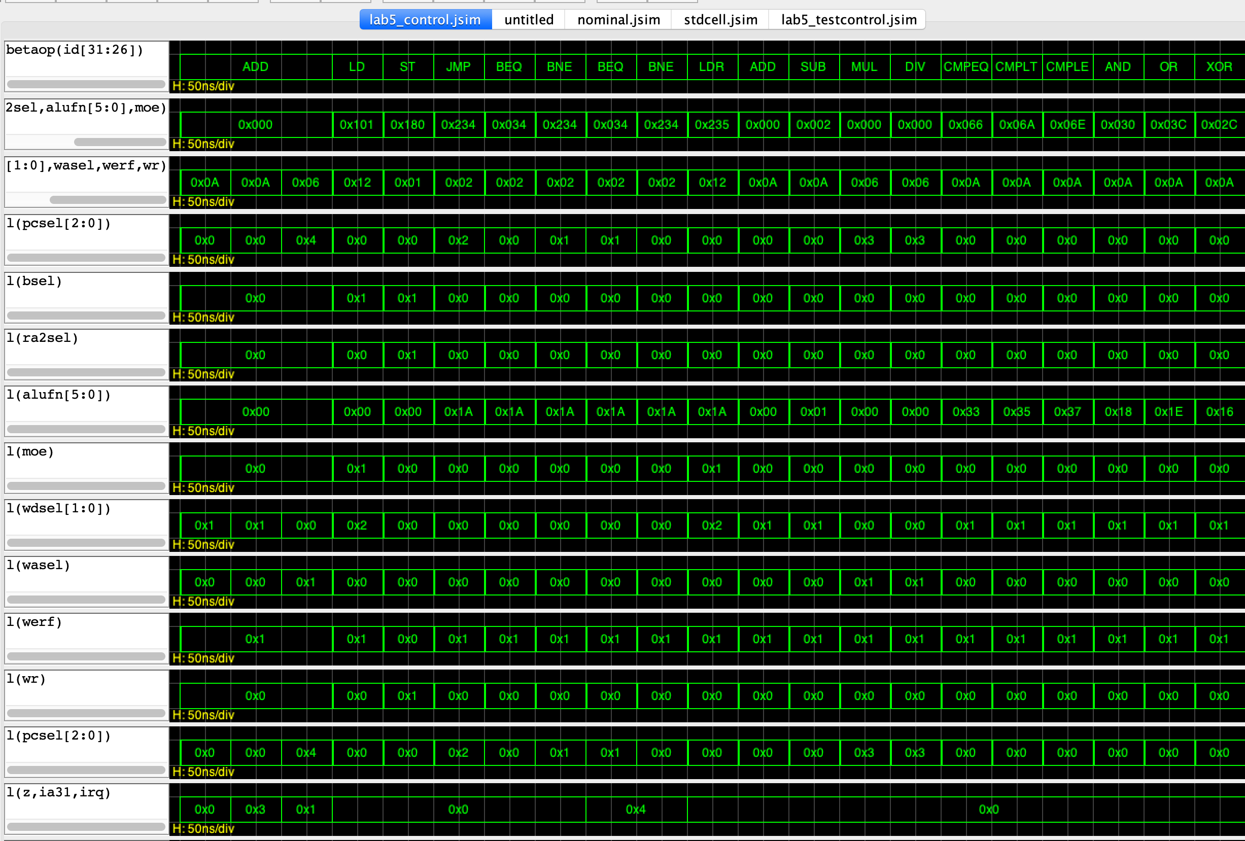
The following window should show up when everything in the control unit works as expected:
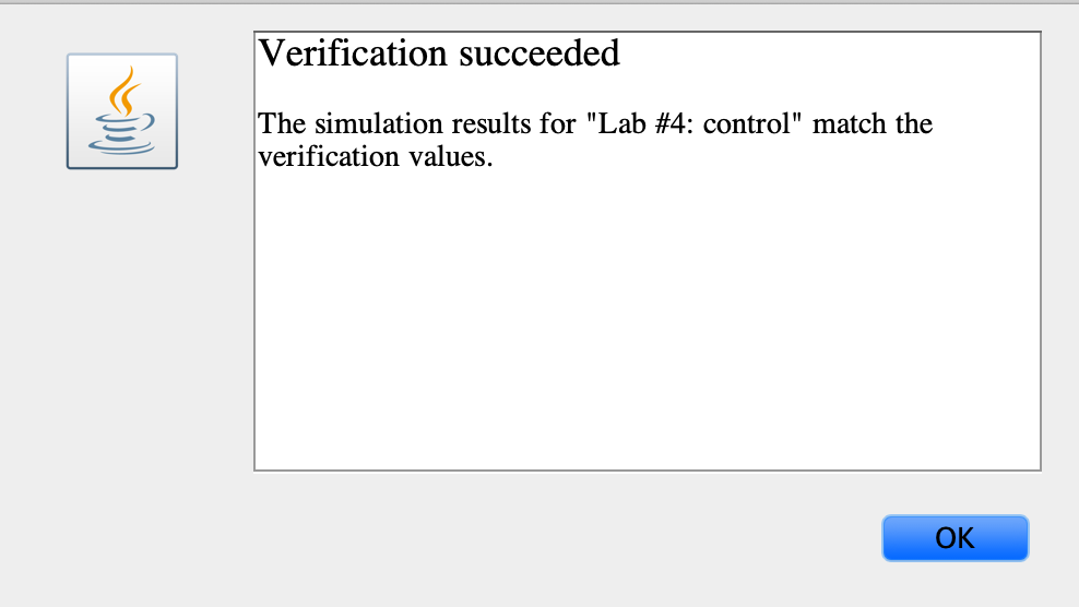
IMPORTANT: comment back the header and the test instructions after you are done. The file lab4_control.jsim should only contain the definition of your pc unit subcircuit only. We will import it later inside lab4_beta.jsim.
ALU + WDSEL Unit
This unit is fairly straightforward to implement. In fact, it is so easy and we just implement it for you inside lab4_aluwdsel.jsim. We reuse ALU implementation from Lab 3, which we have given to you inside lab4_alu.jsim.
ALU+WDSEL Unit Schematic
Here is the suggested ALU + WDSEL Unit schematic that we implement:
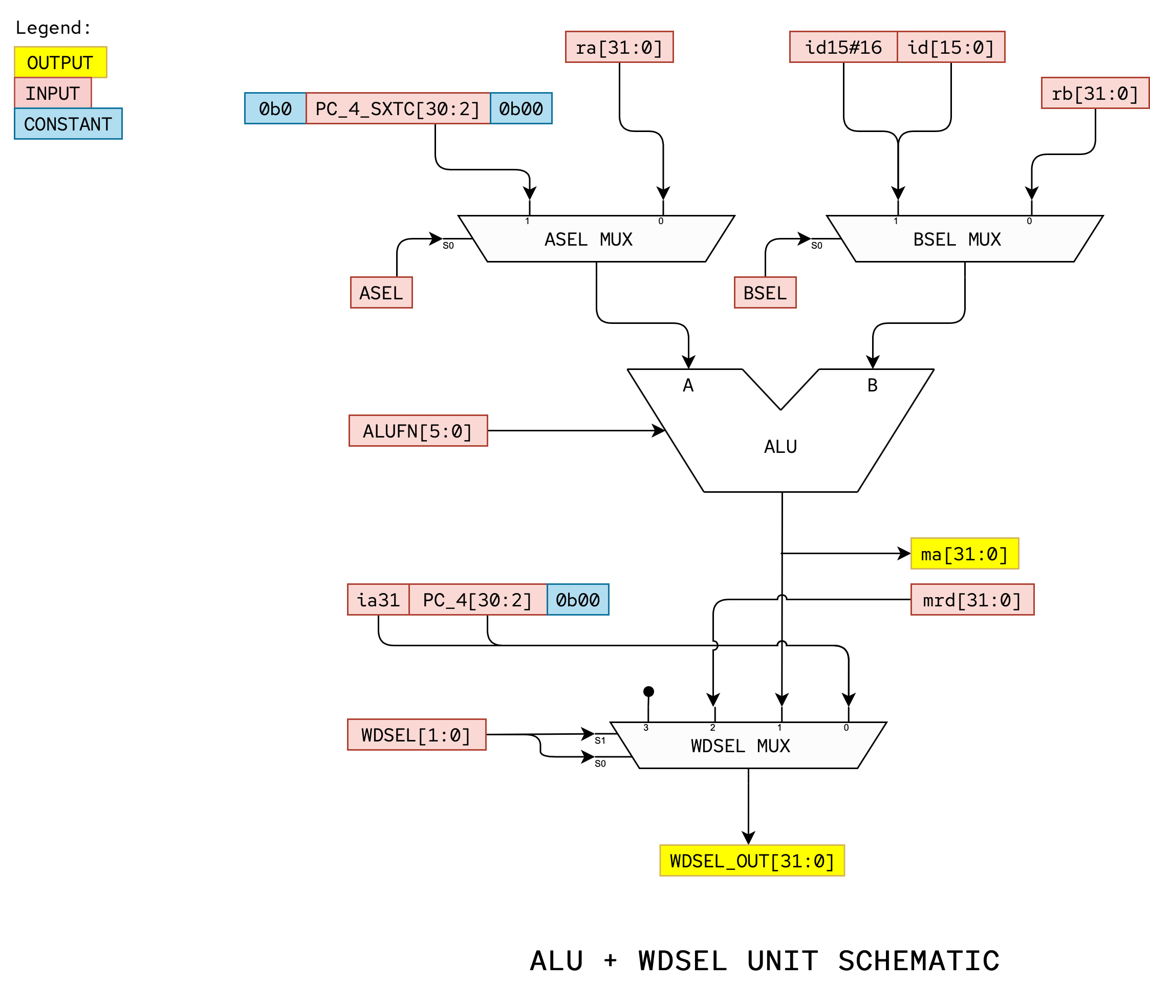
Open lab4_aluwdsel.jsim and observe that the module interface has been provided for you. We follow the ALU+WDSEL Unit Schematic above for the declaration of the input and output (they are positional arguments):
1
2
3
4
.subckt ALUWDSEL_UNIT ia31 id[15:0] ra[31:0] rb[31:0] PC_4[31:0] PC_4_SXTC[31:0] ASEL BSEL ALUFN[5:0] WDSEL[1:0] mrd[31:0] ma[31:0] WDSEL_OUT[31:0]

...
.ends
ASEL and BSEL Mux
The low-order 16 bits of the instruction need to be sign-extended to 32 bits as an input to the BSEL mux. Sign-extension is easy in hardware, no extra components needed as you have known already when creating the shift+add component in PC Unit.
Also, Bit 31 of the branch-offset input to the ASEL mux should be set to 0. This means that the supervisor bit is ignored when doing address arithmetic for the LDR instruction.
WDSEL Mux
Bit 31 of the PC+4 input to the WDSEL mux should connect to the highest bit of the PC Reg output, ia31, saving the current value of the supervisor whenever the value of the PC is saved by a branch instruction or trap.
Please study the circuitry inside
lab4_aluwdsel.jsimbefore proceeding to the next section.
Task D: Assemble Completed Beta
Open lab4_beta.jsim and notice that it should have these .include statements:
1
2
3
4
5
6
7
8
9
.include "nominal.jsim"
.include "stdcell.jsim"
.include "lab4_control.jsim"
.include "lab4_pc.jsim"
.include "lab4_regfile.jsim"
.include "lab4_aluwdsel.jsim"
.include "lab4_adder.jsim"
.include "lab4_alu.jsim"
.include "lab4checkoff.jsim"
and the following subcircuit definition:
1
2
3
4
5
6
7
8
9
10
11
12
.subckt beta clk reset irq ia[31:0] id[31:0] ma[31:0] moe mrd[31:0] wr mwd[31:0]
* BEGIN ANSWER
* initialise pc unit circuit

* initialise regfile unit circuit

* initialise control unit circuit

* initialise alu+wdsel unit circuit

* END ANSWER
.ends
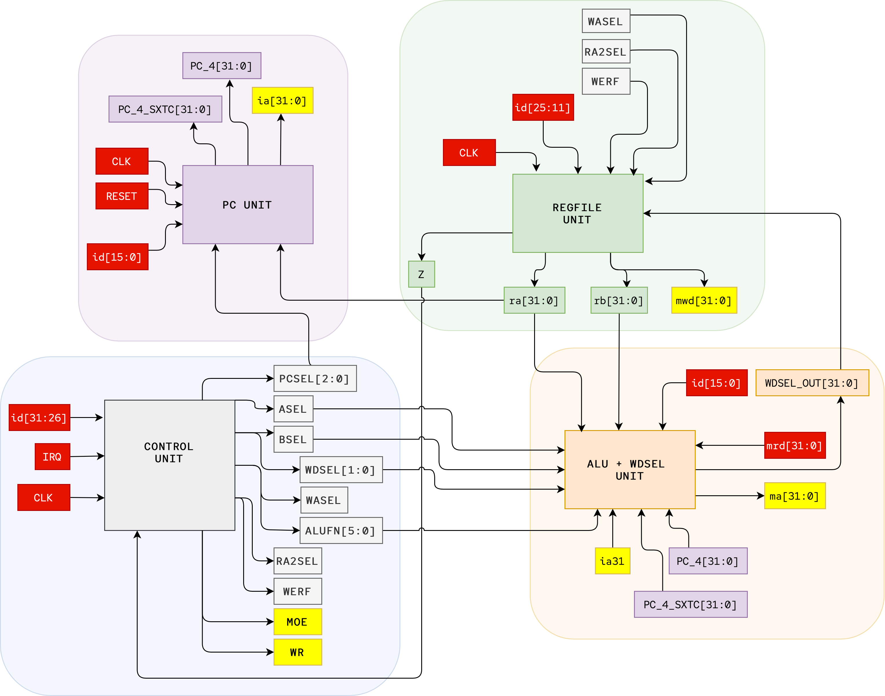
The complete schematic of the Beta is (you might want to open this image in another tab):
Note the addition of the IRQ (interrupt request) input. Your design will be tested at a cycle time of 100ns. The reset signal is asserted for the first clock edge and then deasserted to start the program running. This implementation of the Beta subcircuit has the following terminals:
1
2
3
4
5
6
7
8
9
10
	clk		input		clock (from test circuitry)
	reset		input		reset (from test circuitry)
	irq		input		interrupt request (from test circuitry)
	ia[31:0]	outputs	        instruction address (from PC register)
	id[31:0]	inputs		instruction data (from test circuitry)
	ma[31:0]	outputs	        memory data address (from ALU)
	moe		output		memory read data output enable (from control logic)
	mrd[31:0]	inputs		memory read data (from test circuitry)
	wr		output		memory write enable (from control logic)
	mwd[31:0]	outputs	        memory write data (from register file)
When you have completed your design, you can use lab4checkoff.jsim to test your circuit and complete the checkoff. lab4checkoff.jsim uses the following netlist to create the test circuitry, and checks out your design by attempting to run a test program and verifying that your Beta outputs the correct value on its outputs every cycle.
1
2
3
4
5
6
7
8
9
10
11
12
13
14
15
16
17
18
19
20
21
22
23
24
25
26
27
28
29
30
31
32
33
34
// create an instance of the Beta to be tested
Xbeta clk reset irq ia[31:0] id[31:0] ma[31:0]
+ moe mrd[31:0] wr mwd[31:0] beta

// memory is word-addressed and has 1024 locations
// so only use address bits [11:2].  moe
Xmem
+ vdd 0 0 ia[11:2] id[31:0]     // port 1: instructions (read)
+ moe 0 0 ma[11:2] mrd[31:0]    // port 2: memory data (read)
+ 0 clk wr ma[11:2] mwd[31:0]   // port 3: memory data (write)
+ $memory width=32 nlocations=1024 contents=(
+ … binary representation of /50002/lab4.uasm …
+ )

// clock has 100ns cycle time, starts as 1 so first clock
// edge happens 100ns into the simulation
Vclk clk 0 pulse(3.3,0,49.9ns,.1ns,.1ns,49.9ns,100ns)

// reset starts as 1, set to 0 just after first clock edge
Vreset reset 0 pwl(0ns 3.3v, 101ns 3.3v, 101.1ns 0v)

// interrupt request is asserted twice.  The first time (during
// cycle 10) should be ignored because the Beta is in supervisor
// mode, the second time (during cycle 273) should cause an
// interrupt.
Virq irq 0 pwl(0ns 0v, 1001ns 0v,
+ 1001.1ns 3.3v,
+ 1101ns 3.3v,
+ 1101.1ns 0v,
+ 27301ns 0v,
+ 27301.1ns 3.3v,
+ 27401ns 3.3v,
+ 27401.1ns 0v
+)
The source for the test program can be found here, a file called
lab4.uasm.You don’t need to read this if you don’t wish to.
The checkoff program attempts to exercise all the features of the Beta architecture. If this program completes successfully, it enters a two-instruction loop at locations 0x3C4 and 0x3C8. It reaches 0x3C4 for the first time on cycle 277.
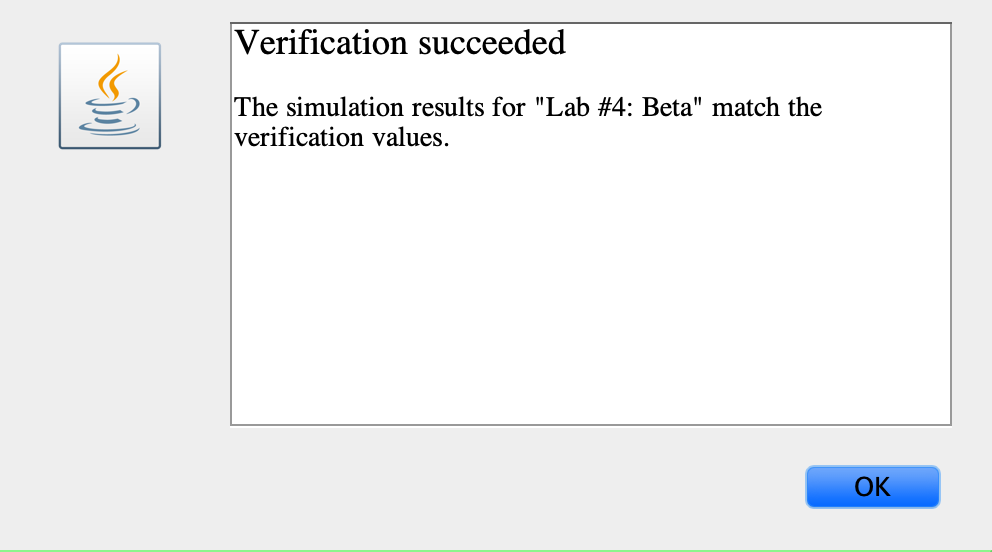
lab4checkoff.jsim will VERIFY that the instruction address (ia[31:0]), memory address (ma[31:0]), memory write data (mwd[31:0]) and the memory control signals (moe, wr) have the correct values each cycle.
You should see a window popped up as such after running the simulation.
Click the green tick on the upper right corner to see if you get all supposed output.
If all expected values are correct, you should see the following window pops up after you click the tick sign:
IMPORTANT: Ensure that you comment out any custom test circuit in the other lab4_[component].jsim files and comment out all header includes. Else you will be met with duplicate device name error if you attempt to import the same module twice in two different .jsim files.
The check is made just before the rising clock edge, i.e., after the current instruction has been fetched and executed, but just before the result is written into the register file. Note that ma[31:0] is the output of the ALU, so these checks can verify that all instructions are working correctly.
Almost nobody’s design executes the checkoff program correctly the first time! To understand what went wrong, you’ll need to retrieve the error code and compare it with the table given at the beginning of
lab4.uasm. The table will indicate at what label the program detected an error; for example if the error code is 0x288, then the checkoff program detected an error in the code just before label “bool1” in the program. Looking through lab4.uasm, you can locate the “bool1” label and see what results the program expected. Now look at the waveforms of your Beta executing the same code and you can usually track down the error in your design. It will take some effort to debug your design, but stick with it! If you’re stuck, get help from your fellow students or the course staff. When it works, congratulate yourself: the design of a complete CPU at the gate-level is a significant accomplishment. Of course, now the fun is just beginning—there are undoubtedly many ways you can make improvements, both large and small. Good luck!
Appendix 1: The cycle time of your Beta
If your design contains any registers or memories, JSim will report the “minimum observed setup time” at the end of each simulation run.
- At each rising clock edge, JSim determines the setup time for each data input to a register or memory (i.e., how long the data inputs were valid before the rising clock edge).
- JSim remembers the smallest setup time it finds, along with the simulated time it made the observation and the device involved. So, for example, JSim might report:
min observed setup = 85.235ns @ time=5.2us (device = xbeta.xregfile)
For a Beta design, the reported device is almost always the register file. This makes sense since the last signals to settle should be WDATA[31:0], the data inputs to the register file.
Since the tests are run with a clock period of 100ns, this tells us that we could have reduced the clock period to (100 – 85.235 + tMEM SETUP)ns and still expect the test program to run correctly. We can look at the waveform plots to determine what instruction had just finished executing at time 5.2us – that’s the instruction whose execution we’d have to speed up in order to reduce the cycle time of our Beta.
Typically the worst-case execution time comes from either CMPxx or LD instructions (why?).
Using this technique, investigate where the critical path(s) are in your Beta design and work to make them as short as possible. To get the fastest possible cycle time you’ll probably need to implement some of your control signals (e.g., RA2SEL) using logic gates rather than a ROM. Given that we might have to make three memory accesses in a single cycle (instruction fetch + register file access + data memory access = 10ns total assuming a 1024-location main memory), we won’t be able to do better than 100Mhz clock rates unless we pipeline our implementation.
Appendix 2: Using the JSim memory component
We will be using a new component in this lab: a multi-port memory. JSim has a built-in memory device that can be used to model memories with a specified width and number of locations, and with one or more ports. Each port has 3 control signals and the specified number of address and data wires. You can instantiate a memory device in your circuit with a statement of the form:
1
Xid ports… $memory width=w nlocations=nloc options…
The width and nlocations properties must be supplied:
- w specifies the width of each memory location in bits and must be between 1 and 32.
- nloc specifies the number of memory locations and must be between 1 and \(2^{20}\).
All the ports of a memory access the same internal storage, but each port operates independently.
Each port specification is a list of nodes:
1
oe clk wen a[naddr-1] … a[0] d[w-1] … d[0]
where:
oeis the output enable input for a READ port.- When 1, data is driven onto the data pins;
- When 0, the output pins are not driven by this memory port.
- If this port is only a write port, connect this terminal to the ground node “0”.
- If the port is only a read port and should always be enabled, connect this terminal to the power supply node “vdd”.
-
wenis the write enable input for WRITE ports.- See the description of
clkfor details about the write operation. If this port is only a read port, connect this terminal to the ground node “0”.
- See the description of
-
clkis the clock input for WRITE ports.- When
wen=1, data from the data terminals is written into the memory on the rising edge of clk. - If this port is only a read port, connect this terminal to the ground node “0”.
- When
-
a[naddr-1] … a[0]are the address inputs, listed most significant bit first.- The values of these terminals are used to compute the address of the memory location to be read or written.
- The number of address terminals is determined from the number of locations in the memory:
naddr = ceiling(log2(nloc)). - When the number of locations in a memory isn’t exactly a power of 2, reads that refer to non-existent locations return “X” and writes to non-existent locations have no effect.
d[w-1] … d[0]are the data inputs/tristate outputs, listed most significant bit first.
By specifying one of the following options it is possible to specify the initial contents of a memory (if not specified, the memory is initialized to all X’s):
-
file="filename": The memory is initialized, location-by-location, from bytes in the file.- Data is assumed to be in a binary little-endian format, using
ceiling(w/8)bytes of file data per memory location. - Bits 0 through 7 of the first file byte are used to initialize bits 0 through 7 of memory location 0, bits 0 through 7 of the second file byte are used to initialize bits 8 through 15 of memory location 0, and so on.
- When all the bits in a memory location have been filled, any bits remaining in the current file byte are discarded and then the process continues with the NEXT memory location.
- In particular, the “.bin” files produced by BSim can be used to initialize JSim memories.
For example, the following statement would create a 1024-location 32-bit memory with three ports: 2 READ ports and 1 one WRITE port. The memory is initialized from the BSim output file “foo.bin”.
- Data is assumed to be in a binary little-endian format, using
1
2
3
4
5
6
Xmem
+ vdd 0 0 ia[11:2] id[31:0]    // (read) instruction data
+ vdd 0 0 ma[11:2] mrd[31:0]   // (read) program data (LDs)
+ 0 clk wr ma[11:2] mwd[31:0]  // (write) program data (STs)
+ $memory width=32 nlocations=1024
+ file="foo.bin"
contents=( data… )- The memory is initialized, location-by-location, from the data values given in the list.
- The least significant bit (bit 0) of a value is used to initialize bit 0 of a memory location, bit 1 of a value is used to initialize bit 1 of a memory location, and so on.
- For example, to enter the short test program ADDC(R31,1,R0); ADDC(R31,2,R1); ADD(R0,R1,R2) one might specify:
1
2
3
4
5
6
Xmem
+ vdd 0 0 ia[11:2] id[31:0]    // (read) instruction data
+ vdd 0 0 ma[11:2] mrd[31:0]   // (read) program data (LDs)
+ 0 clk wr ma[11:2] mwd[31:0]  // (write) program data (STs)
+ $memory width=32 nlocations=1024
+ contents=(0xC01F0001 0xC03F0002 0x80400800)
Initialized memories are useful for modeling ROMs (e.g., for control logic) or simply for loading programs into the main memory of your Beta.
One caveat: if the memory has a write port and sees a rising clock edge with its write enable not equal to 0 and with one or more of the address bits undefined (i.e., with a value of “X”), the entire contents of the memory will also become undefined.
So you should make sure that the write enable for a write port is set to 0 by your reset logic before the first clock edge, or else your initialization will be useless.
The following options can be used to specify the electrical and timing parameters for the memory. For this lab, these should NOT be specified and the default values should be used.
-
tcd=seconds: the contamination delay in seconds. Default value = 20ps. -
tpd=seconds: the propagation delay in seconds. This is how long it takes for changes in the address or output enable terminals to be reflected in the values driven by the data terminals. Default value is determined from the number of locations: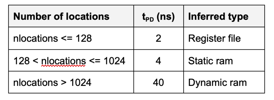
-
tr=seconds_per_farad: the output rise time in seconds per farad of output load. Default value is 1000, i.e., 1 ns/pf. -
tf=seconds_per_farad: the output fall time in seconds per farad of output load. Default value is 500, i.e., 0.5 ns/pf. -
cin=farads: input terminal capacitance in farads. Default value = 0.05pf. -
cout=farads: output terminal capacitance in farads. Default value = 0pf (additional tPD due to output terminal loading is already included in default tPD).
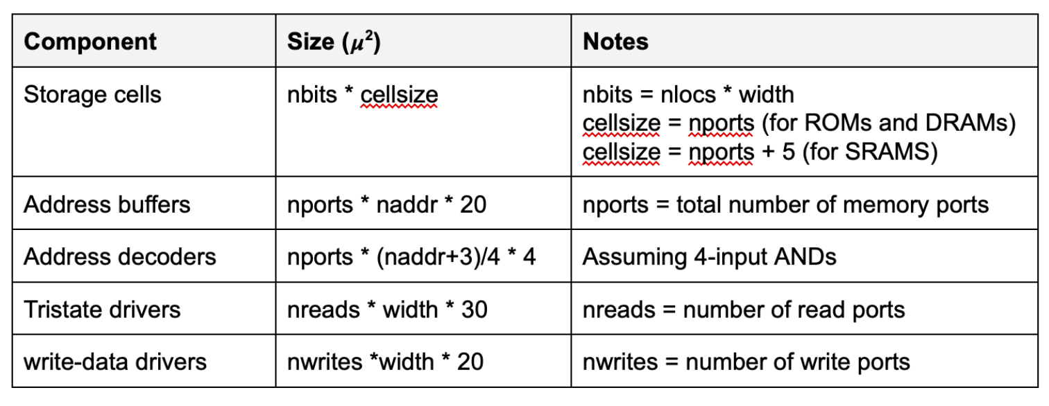
The size of a memory is determined by the sum of the sizes of the various memory building blocks shown in the following table:
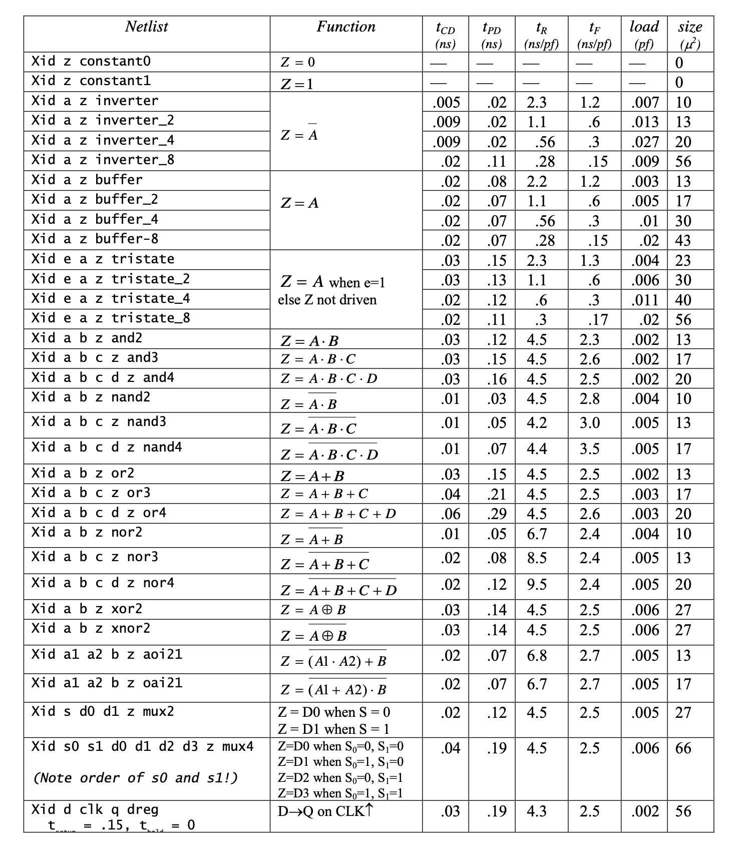
Appendix 3: Standard Cells
For your convenience, we provide to you the specs for stdcell.jsim components: