
- TOC
50.002 Computation Structures
Information Systems Technology and Design
Singapore University of Technology and Design
Modified by: Kenny Choo, Natalie Agus, Oka Kurniawan (2021)
Lab 2: Adder
Starter Code
The following files inside your /50002/ folder are what you’re going to open and modify or study for this lab, then submit (unless otherwise stated):
lab2_submit.jsimlab2_debug.jsim(for debugging only, no submission required)
Related Class Materials
The lecture notes on CMOS technology and logic synthesis are closely related to this lab.
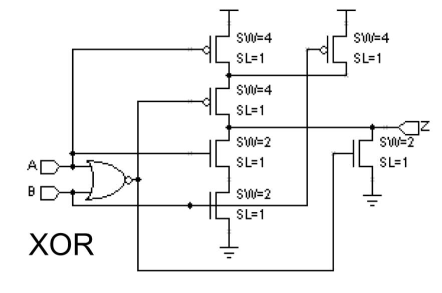
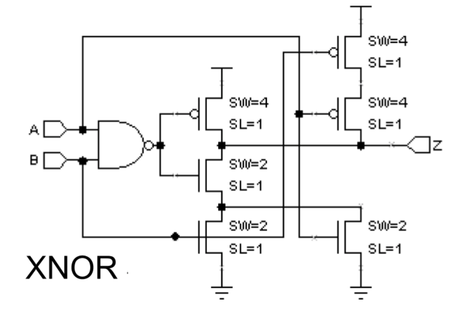
Task A: Building XOR and XNOR gate using PFETs and NFETs
Related sections in the notes:
- Logic Synthesis:
- N-input gates (other gates you can use to build a FA)
- Logic Synthesization with CMOS (you can build a XOR or XNOR using CMOS)
- CMOS Technology:
- Understand why the C in CMOS is necessary: to prevent short circuit; the PU and PD cannot both be ON.
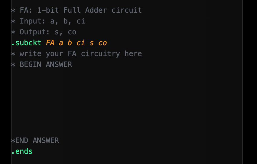
Task B: Build 1-bit Full Adder using gates you built in Task 1
Related sections in the notes: (logic synthesis)
- Sum-of-products (you can build a FA using AND, OR, and INV gates)
- Universal gates (you can build a FA using NANDs only or NORs only)
- Realise that there’s more than ONE way to construct a FA circuit. There’s no one right or best circuit.
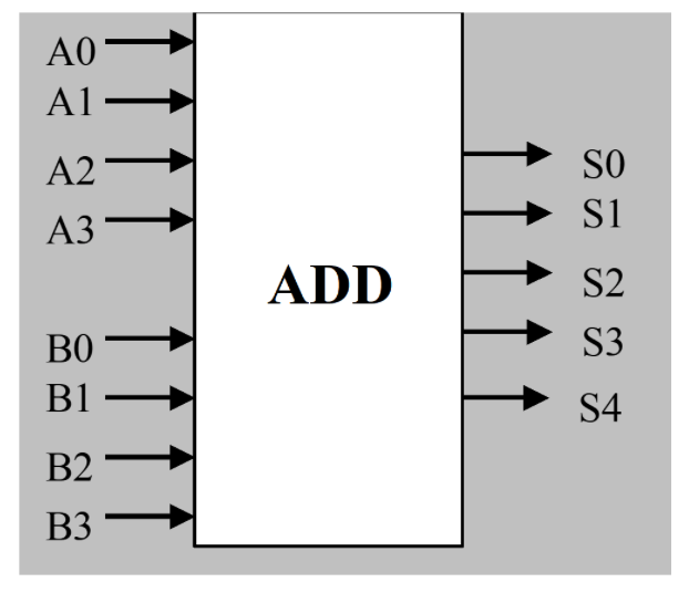
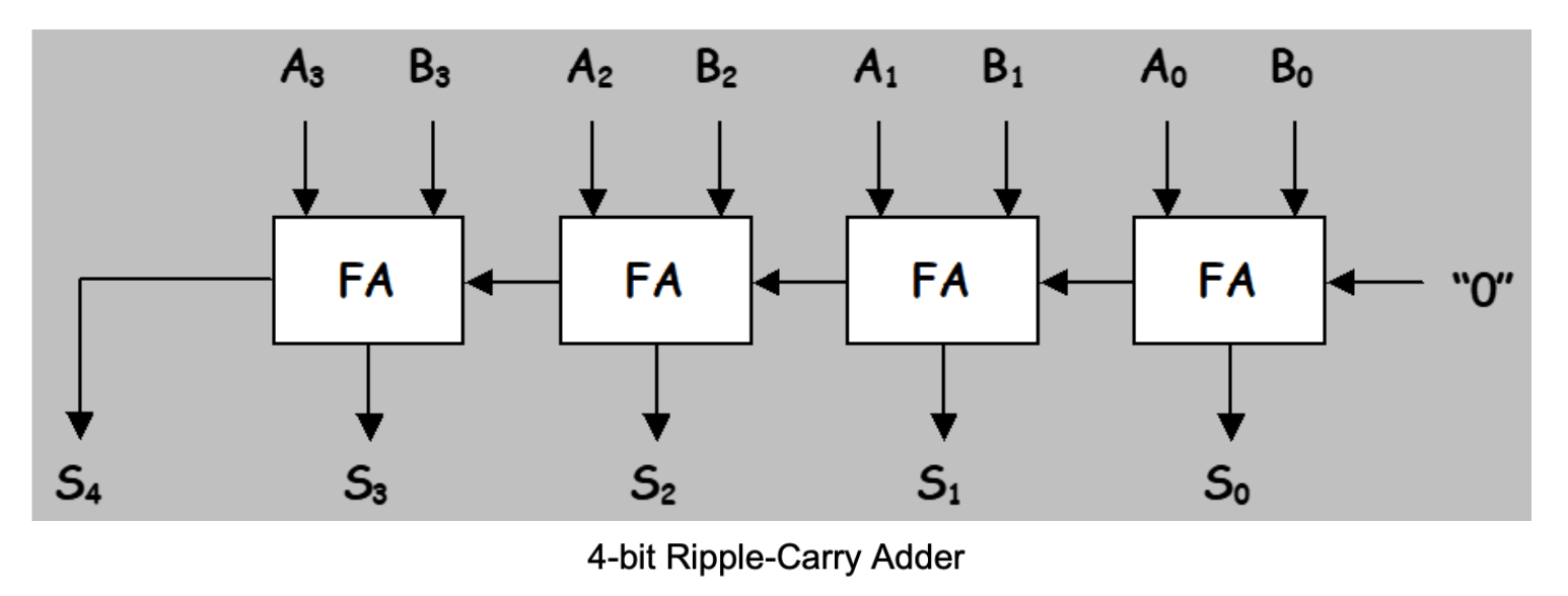
4-bit Ripple Carry Adder
Your mission this week is to design and test a CMOS circuit that performs addition on TWO UNSIGNED 4-bit inputs: A[3:0], B[3:0], producing a 5-bit output S[4:0]:
Task A: Building Logic Gates XOR and XNOR (50 mins)
Since logic gates are used to implement the logic for the full adder, a good place to start is to:
- Build your own gate library (e.g., inverter, 2-input
nand, 2-inputnor,inv, 2-inputxnor, 2-inputxor), - Test them individually, then
- Use them to implement your design.
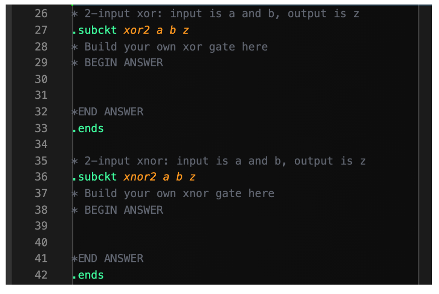
We have given you a headstart by implementing 2-input nand, 2-input nor, and inv for you inside lab2_submit.jsim. Now you just need to implement 2-input xnor and 2-input xor gates.
XOR and XNOR Gate Schematic
It’s much easier to debug your circuit module-by-module rather than as one big lump. XOR/XNOR can be challenging gates to design; here’s one suggestion for how they might be implemented. Use PFET with specs: SW as 4 and SL as 1, and NFET with specs: SW as 2 and SL as 1.
Task B: Simple 1-bit Adder (30 mins)
Let’s start a simple 1-bit full-adder module before proceeding to create a 4-bit Ripple-Carry adder. Later we will discuss higher performance adder architectures you can use in the implementation of the Beta (the computer central processing unit we will be designing in later labs).
The full adder module has 3 inputs (A, B, and Ci) and 2 outputs (S and Co). The logic equations and truth tables for S and Co are shown below.
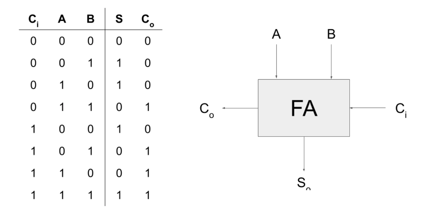
Logic Equation:
\[\begin{align} S &= A \oplus B \oplus C_{i} \\ C_{o} &= A \cdot B + A \cdot C_{i} + B \cdot C_i \end{align}\]Hints:
- S is typically implemented using two cascaded 2-input XOR gates.
- You can use three 2-input NANDs and one 3-input NAND to implement Co (remember that by De Morgan’s Law, two cascaded NANDs are logically equivalent to a cascade of AND/OR).
Ripple-Carry Adder
We can cascade FA units to form Ripple-Carry Adder. The module performs the addition of two one-bit inputs (A and B) incorporating the carry in from the previous stage (Ci). The result appears on the S output and a carry (Co) is generated for the next stage.
A possible schematic for the 4-bit adder is shown below:
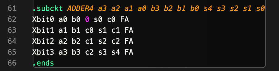
We have implemented this part for you inside lab2_submit.jsim. Please study it.
Testing your Circuit
The file lab2_debug.jsim contains code to debug and test your circuit. You DO NOT need to submit this file.
You can use the file 8clocks.jsim which can be included in your netlist to generate test waveforms for your circuits. It provides eight different square waves (50% duty cycle) with different periods:
1
2
3
4
5
6
7
8
clk1	period = 10ns
clk2  	period = 20ns
clk3  	period = 40ns
clk4  	period = 80ns
clk5  	period = 160ns
clk6  	period = 320ns
clk7  	period = 640ns
clk8  	period = 1280ns
For example, to completely test all possible input combinations for a 2-input gate, you could connect clk1 and clk2 to the two inputs and simulate for 20ns. See lab2_debug.jsim file for example. You can open lab2_debug.jsim and click the Fast Transient Analysis button. Comment out the line .include "lab2checkoff.jsim" in lab2_submit.jsim if you want to plot these debug plots instead of the checkoff plots. Don’t forget to uncomment back this line for your final submission..
Below is a screenshot on the contents of lab2_submit.jsim:
- In
lab2_debug.jsim, we useclk1,clk2, andclk3to create signals forA,B, andCiusing an inverter (you can use a buffer too, it doesn’t really matter). - Since each clock period is double the previous one, we will be able to create all 8 input combinations:
000, 001, …, 111using these three clocks. - Then we plug in
A,B, andCisignals to FA, getting its output:S, andCo. - Afterwards, we plot them (line 11-15).
Once you are somewhat confident that your circuit works properly, go to lab2_submit.jsim and click the Fast Transient Analysis (not device level simulation!) button. A window as such should pop up:
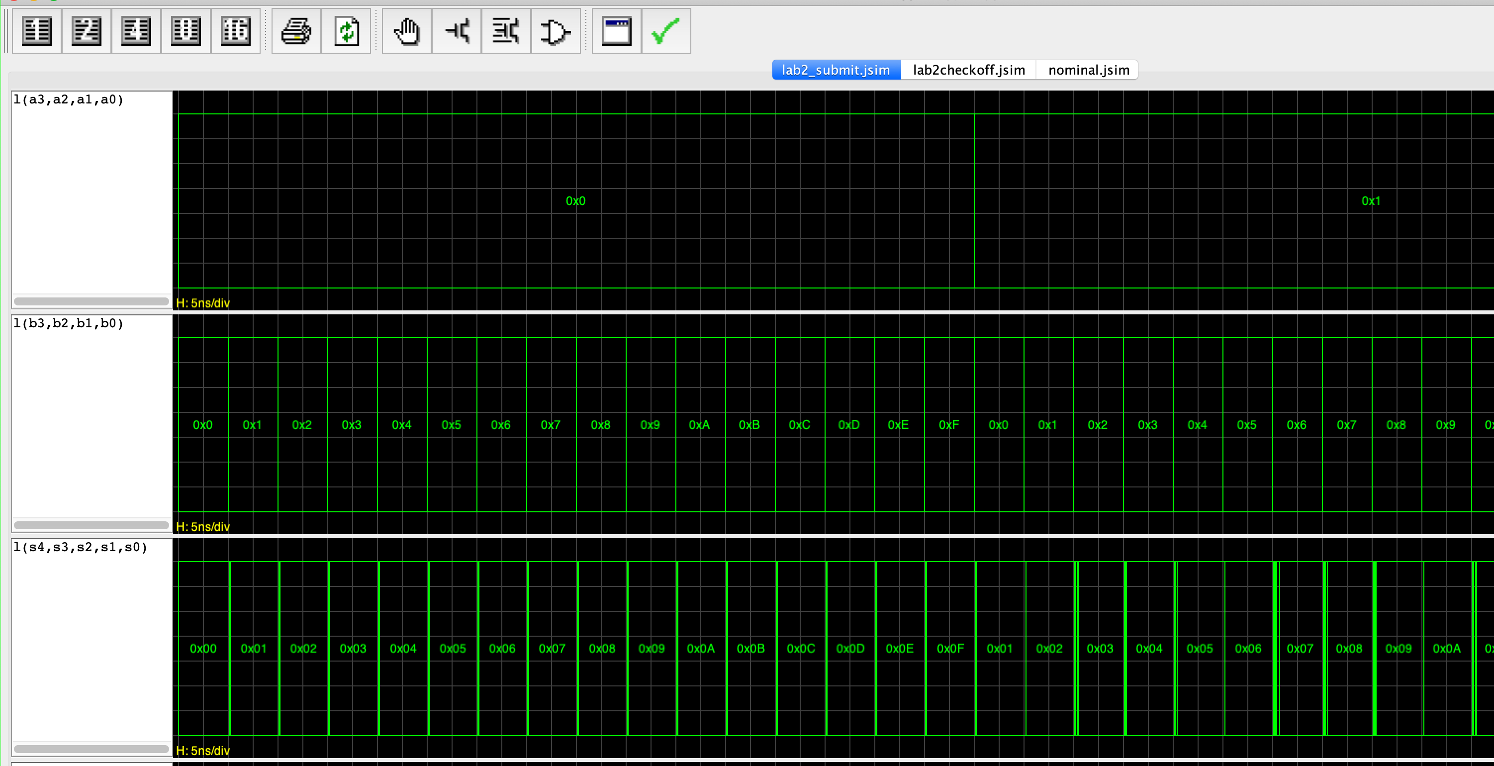 This plot represents all signals produced by
 s[4:0] given various a and b values as time progresses (time is the x-axis). You can zoom in to see the plots better.
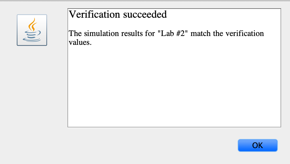
Click on the top right hand corner green tick button to check if all values are as expected. If everything works correctly, this window should pop up:
Appendix: Interpreting analogue signal levels using JSim
Interpreting analog signal levels as logic values can be tedious. For a given signal a, JSim will do it for you automatically if you ask to plot L(a) instead of just a. The logic-high and logic-thresholds are determined by the vih and vil options:
1
.options vih=2.6 vil=0.6
These values are already specified in nominal.jsim, but you can override them in your own netlist. Voltages between vil and vih are displayed as a filled-in rectangle to indicate that the logic value cannot be determined (invalid values). For example:
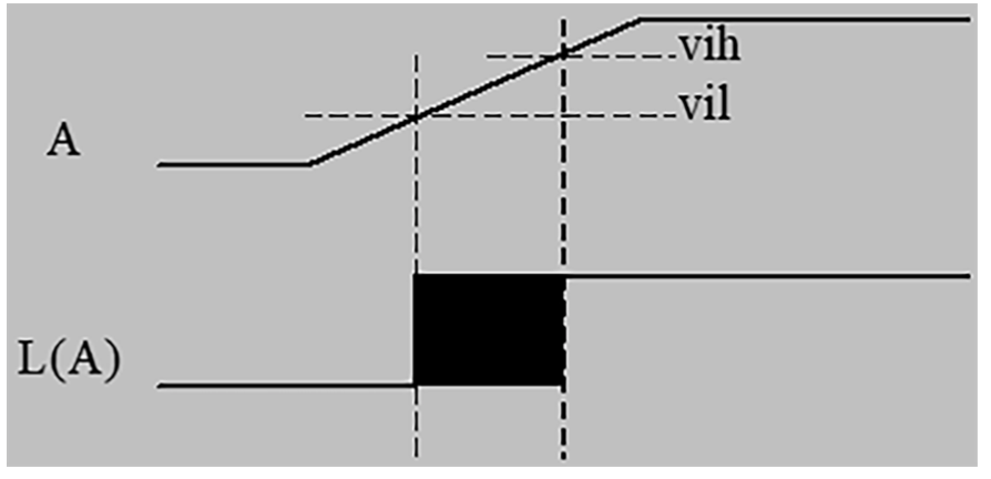
You can also ask for the values of a set of signals to be displayed as a bus, e.g., L(a3,a2,a1,a0). The signals should be listed, most-significant bit first. A bus waveform is displayed as a:
- Filled-rectangle if any of the component signals has an invalid logic level or
- As a hexadecimal value if it has a valid logic level.

There are three sections to the above plot:
- Initially, the four signals
a3,a2,a1anda0are interpreted as a 4-bit integer with initial value of1111 (0xF). - Then, since x-axis represents time, the high-order bit (
a3) is making a 1→0 transition.- The filled-in rectangle represents the period of time during which
a3transitions from Vih to Vil, rendering them ALL invalid denoted in the shaded rectangle - If one signal is invalid, all signals in the bus will be deemed invalid as a shaded box!,
- The filled-in rectangle represents the period of time during which
- After the highest bit made a transition to zero completely, and the value of L ultimately became valid
0111 (0x7).
Below is the screenshot of the JSIM plot that you will see after you complete your code and would like to test the answer. You can use the plot to check if your code implements the functional specification of a 4-bit adder correctly. Each row is a plot of the values of the terminals over time. For simplicity, they’re represented in hex instead of in binary.
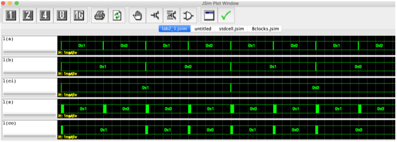
You can represent a which is just 1 bit in hex too. The value of a is periodically changed between 1 and 0 (but when represented as hex it becomes 0x1 and 0x0 respectively even though a is ONE bit).
Another example:
- If signal
bis 3 bits in length with a value of101, the hex representation is0x5 - If signal
cis 6 bits in length with a value of11111, the hex representation is0x3F
The above plot is merely a digital value representation of the signal in hex.
- The value of
bandciis initially 0 - The expected output when
a=1,b=1, andci = 1iss=1andc0=1. We know this from the truth table. - The plot confirms that this is true since the values of
sandc0are shown to indeed be 1 given that combination ofa=1,b=1, andci=1(bottom two rows)