 Computation Structures
50.002 Computation Structures
Information Systems Technology and Design
Singapore University of Technology and Design
Natalie Agus (Fall 2020)
Getting Good with FPGA: Building the Beta CPU
This document is created for the sake of enhancing our understanding in how basic CPU works by actually implementing it onto an FPGA. We will create our 32-bit $\beta$ CPU and use simple dual-port RAM to simulate some of the instructions that we have learned in class and test if they’re working properly.
You are recommended to read this document only after you’ve understood completely up until the chapter on $\beta$ datapath and are comfortable enough with HDL programming:
- You’re confident with your understanding about sequential logic and synchronization.
- You’re comfortable with how memory read and write works, and memory addressing.
- You know how to use common components like
counter,edge detector,button conditioner, andfsmproperly.
If not, please brush up your FPGA programming knowledge by starting with this document instead.
The completed project can be found here, if you want to dive into it right away.
Creating a Memory Unit
You can use a bunch of dffs as a memory unit, but its going to take a lot of the logic cells of your FPGA. Let’s do the math:
- The $\beta$ CPU is a 32-bit architecture.
- If you want your memory unit to support 128 words, then you need 32 $\times$ 128
dffs = 4096dffs. If we’re being optimistic and assume that 1dffuse 1 logic cell, that’s alot of logic cells used simply for the memory unit (about 12% of the Au’s cells).
We shall use another component instead: simple_ram or simple_dual_ram. The difference is that in simple_dual_ram you can perform read and write at the same clock cycle, whereas in simple_ram you only have 1 address port for either read or write.
To create a memory unit, you can first import the component simple_dual_ram (under memory) to your project. You can instantiate a memory unit like this:
simple_dual_ram memory_unit(#SIZE(16), #DEPTH(128), .wclk(clk), .rclk(clk)); // 128 entries (words), 16 bits each
- The parameter
#SIZE(word size) and#DEPTH(entries) can be set accordingly, depending on how many bits you want to have per entry. wclkandrclkare read and write clk. You can set it to be the same as the system clock.
You need to always supply these four inputs to the memory unit. The names are explanatory:
memory_unit.waddr = <write address>;
memory_unit.write_en = <1 or 0>; // 1 for write, 0 otherwise
memory_unit.write_data = <data to be written>;
memory_unit.raddr = <read address>;
Then it will produce the output:
out = memory_unit.read_data;
-
The memory unit is always reading, depending on what is the current
<read address>. You can simply ignore the.read_dataif you don’t need it. - Number of bits for
.raddr/waddris $\log_2$(DEPTH). - Important documentation:
.read_dataalways produces the output from.raddrsupplied in the previous clock cycle. The documentation says that if you supplied addressAatt=0, then att=1(next clock cycle),Mem[A]is produced at.read_dataport.- If you perform read and write to the same location at the same clock cycle e.g: at
t=0, the result of the data written will be observed only two clock cycles later att=2. Att=1, the old data is still produced at the read port.
You can familiarise yourself first with how the memory unit works using an fsm.
- Perform some writes onto the memory unit, and then
- Get input address
.raddrfrom one of theio_dip - Route the output
.read_dataonto one of theio_led
Refer to this RAM tester module to see how it may be done.
Then, in au_top.luc add the following code:
// instantiate the module
ramtester ram(.clk(clk));
button_conditioner buttonconditioner(.clk(clk));
edge_detector buttonedge (#RISE(1), #FALL(0), .clk(clk));

//... in always block
io_led[0] = io_dip[0]; // connect the DIP switches to the LEDs to observe read address
io_led[0][7] = io_button[0]; // use io_button[0] to "write" data

ram.read_address = io_dip[0][5:0]; // set for read address
ram.write_address = io_dip[1][5:0]; // set for write address
ram.data = c{h00, io_dip[2]}; // set for write data
buttonconditioner.in = io_button[0];  // condition button
buttonedge.in = buttonconditioner.out; // get rising edge
ram.button_enter = buttonedge.out; // pass to ram

io_led[2] = ram.out[15:8]; // show 16-bit ram content over both io_leds
io_led[1] = ram.out[7:0];
How ram_tester is used based on the setting above in au_top.luc:
-
Four data in address
b000000, b000001, b000010, b000011are pre-written by thefsminram_tester. They contain the data:hFFFF, h0FFF, h00FF, h000Frespectively. This is to demonstrate auto write at the beginning (startup). - You can use the least 5 bits of
io_dip[0]to set.radrand observe the output atio_led[2]andio_led[1]. - You can write custom data too. Set write address using
io_dip[1]and write adata usingio_dip[2](won’t be shown on any led). Then pressio_button[0]to allow the ram to “write”.Test it by reading using the same address (set
io_dip[0]to be equal toio_dip[1]when you wrote the data).
Now that we understand how the simple_ram module works, lets create a module that corresponds to this memory unit in the $\beta$ schematic shown our notes:
Note: there’s two read ports, and one write port.
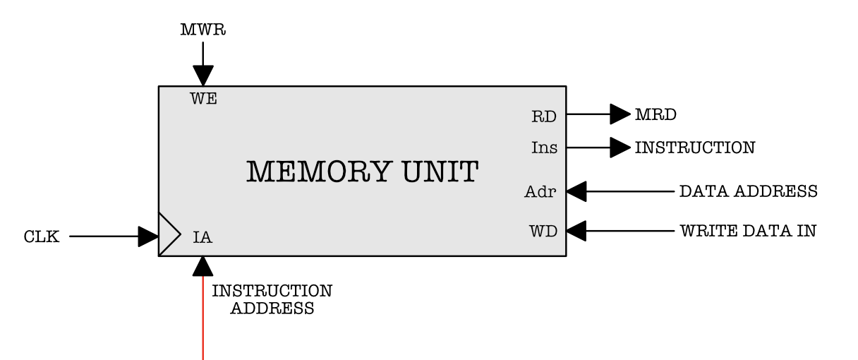
Create a new script memoryunit.luc and define the terminals as follows. The names are self explanatory.
// supports byte addressable
module memoryunit #(
  DEPTH = 16 // entries in the memory
)
(
    input clk,  // clock

    // for data memory
    input raddr[$clog2(DEPTH)+2],
    input waddr[$clog2(DEPTH)+2],
    input data_memory_input[32],
    input xwr,
    output data_memory_output[32],

    // for instruction memory
    input ia[$clog2(DEPTH)+2],
    input instruction_write_enable,
    input instruction_towrite[32],
    output instruction[32]
  )
We will create two ram units as instruction memory and data memory. In practice they’re supposed to be the same memory unit but we don’t have a ram module with two read ports by default, we have to make do with the modules that are available:
Actually since we will never perform data read and data write at the same time, we technically can use
simple_raminstead ofsimple_dual_ramfordata_memory, but we just want to illustrate the usage for both here.
{
  simple_ram instruction_memory(#SIZE(32), #DEPTH(16), .clk(clk)); // can fit 16 * 32 bits
  simple_dual_ram data_memory(#SIZE(32), #DEPTH(16), .wclk(clk), .rclk(clk)); // can fit 16 * 32 bits

  always {

    instruction_memory.write_data = instruction_towrite;
    instruction_memory.address = ia[$clog2(DEPTH)+2-1:2]; // memory_unit is word addressable in Lucid, ignore two LSB
    instruction_memory.write_en = instruction_write_enable;
    instruction = instruction_memory.read_data;

    data_memory.raddr = raddr[$clog2(DEPTH)+2-1:2]; // memory_unit is word addressable in Lucid, ignore two LSB
    data_memory.waddr = waddr[$clog2(DEPTH)+2-1:2];// memory_unit is word addressable in Lucid, ignore two LSB
    data_memory.write_data = data_memory_input;
    data_memory.write_en = xwr;
    data_memory_output = data_memory.read_data;
  }
}
Then in the always block we simply make the correct connections. One thing to pay attention to is the fact that $\beta$ assumes byte-addressable memory unit but the ram modules uses word addressing.
Therefore we need to truncate the two LSB off the addresses supplied by $\beta$: ia (instruction address), radr and wadr (read and write address to the data memory, both are supplied by the same source the output of the ALU).
The complete implementation of memory_unit.luc can be found here.
The ALU
The ALU is a combinational logic unit, so creating it is pretty straightforward.
Just remember that in this document we are recreating the original $\beta$ CPU (32-bit architecture) so we need to create a
32-bitALU instead of the16-bitwe used for 1D project.
We need to ensure that it performs the right operation given an ALUFN input. The unit should have the following input and output terminals:
Don’t forget that
zvnsignals are the also formal output of thealu.module alu ( input a[32], input b[32], input alufn_signal[6], output out[32], output zvn[3] ) )
To make it more interesting, we can follow how we create the ALU in the course lab (instead of writing a bunch of if-elses according to alufn_signal combinations). Create four modules: adder.luc, boolean.luc, shifter.luc, and compare.luc, and implement its functionalities.
The input and output terminals of each module should be exactly as defined in our Lab 3: ALU.
Refer to these completed scripts if you’re stuck: adder, boolean, shifter, compare.
Then assemble all of them in the alu.luc module where you instantiate all of them:
adder adderUnit;
boolean booleanUnit;
shifter shifterUnit;
compare compareUnit;

sig z;
sig v;
sig n;
…and implement the connections in the always block, for instance here’s the connection between the adder and the compare unit:
adderUnit.alufn_signal = alufn_signal;
adderUnit.a = a;
adderUnit.b = b;

z = adderUnit.z;
v = adderUnit.v;
n = adderUnit.n;

zvn[0] = z;
zvn[1] = v;
zvn[2] = n;

compareUnit.alufn_signal = alufn_signal;
compareUnit.z = z;
compareUnit.v = v;
compareUnit.n = n;
You can find the complete implementation of alu.luc here.
The Regfile Unit
The REGFILE unit has 32 32-bit registers, where each register is 5-bit addressable. We have 2 combinational read ports and 1 sequential write port. Also, our special register R31 should always return 32b0 when read, and writing to R31 should not change its value (it remains zero). The schematic for the REGFILE is:
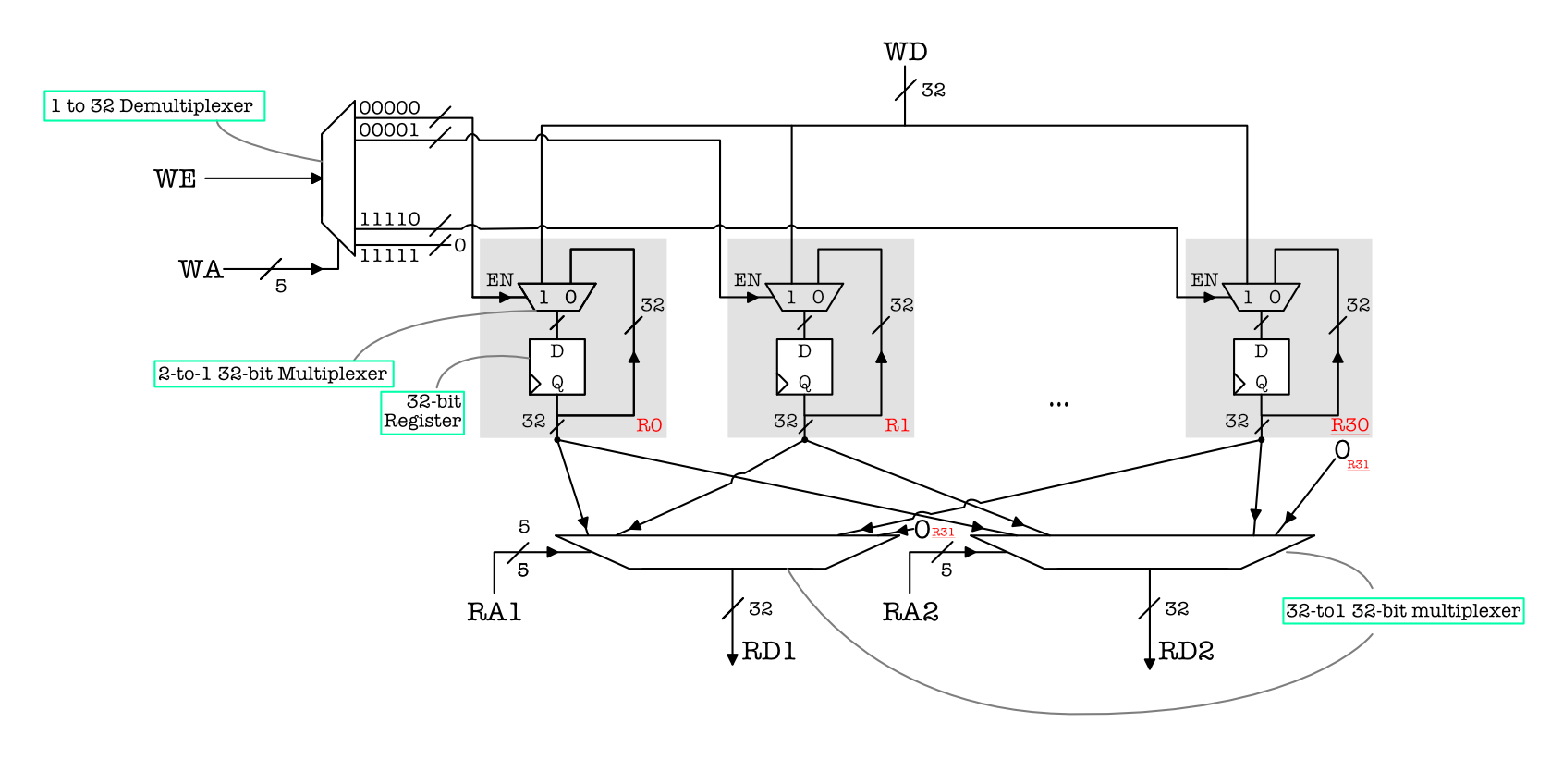
We can easily create a module for this unit using dff. Create a script called regfile.luc with the same I/O terminals:
 module regfile (
    input clk,  // clock
    input read_address_1[5],
    input read_address_2[5],
    output read_data_1[32],
    output read_data_2[32],
    input write_address[5],
    input write_data[32],
    input write_enable
  )
Then we instantiate 32 32-bit dffs to represent R1 to R31. The REGFILE always performs a read at all times, so you can always ignore its output later on if you don’t need it.
Of course we can just instantiate 31
dffinstead of 32. Its your choice. Regardless, always make sure that writing toR31doesn’t have any effect, and reading fromR31always result in32b0.
{
  dff registers[32][32](.clk(clk));
  always {
    //always read
    read_data_1 = registers.q[read_address_1];
    read_data_2 = registers.q[read_address_2];

    // check if write_en and its not R31
    if (write_address != b11111 && write_enable){
        registers.d[write_address] = write_data;
    }

    // check if its not R31
    if (read_address_1 == b11111) read_data_1 = h0000;
    if (read_address_2 == b11111) read_data_2 = h0000;
  }
}
The complete implementation of regfile.luc can be found here.
The Control Unit
Now our job is to create the control unit module. Here’s the schematic of the CU:
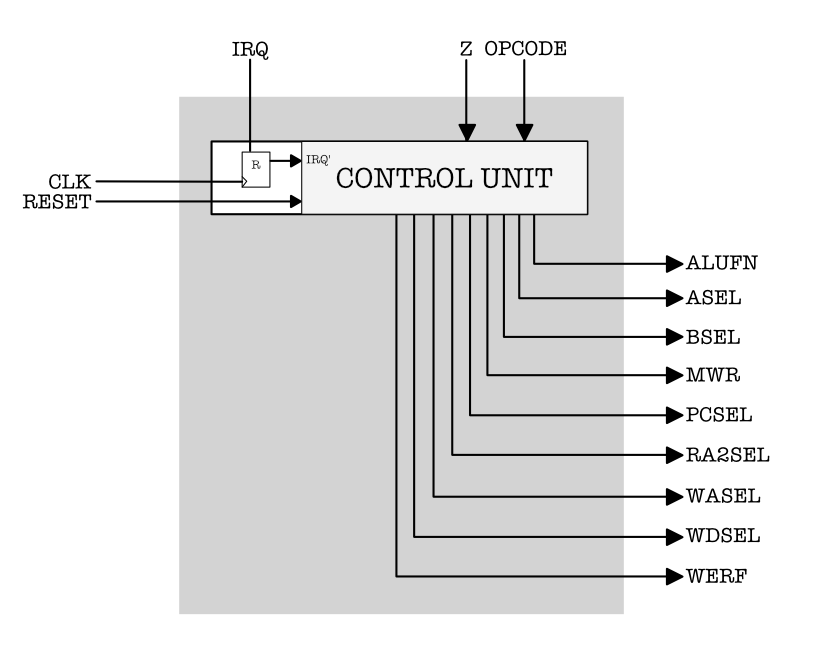
The small 1-bit register’s job is to sample an asynchronous interrupt signal. We can use a 1-bit dff for this:
{
	dff irq_sampler(#INIT(0), .clk(clk));
always {
	irq_sampler.d = irq;
	}
}
To produce the right control signals given an opcode, we can utilize a ROM (64 entries, 18 bits per entry as defined in the Beta lab handout).
Remember the addressing for a ROM in Lucid is as follows:
// usage: CU_ROM[opcode]
const CU_ROM = {
        b011100000000000100, // OPCODE 111111 (illop)
        b000000110001101100, // OPCODE 011110 (SRAC)
        b000000110000101100, // OPCODE 011101 (SHRC)
        ....
        b011100000000000100,
        b011100000000000100,// OPCODE 000001 (illop)
        b011100000000000100	// OPCODE 000000 (illop)
        };
We then need to handle the pcsel value for bne/beq case separately:
    // beq bne handling
    if (opcode == b011101 && z == 1){//BEQ, branch if z == 1
      pcsel = b001;
    }
    else if (opcode == b011110 && z == 0){ //BNE, branch if z != 1
      pcsel = b001;
    }
Similarly, reset and irq cases have to be handled separately. They have to be written at the end of the always block (highest priority).
    // force xwr = 0 when reset == 1
    if (reset){
      xwr = 0;
      werf = 0;
    }

    // interrupt checker, will overwrite everything hence we put at the bottom
    if (irq_sampler.q == 1){
      pcsel = b100;
      wasel = 1;
      werf = 1;
      wdsel = b00;
      xwr = 0;
    }
The complete implementation of control_unit.luc can be found here.
Assembling the Beta
Now that we have all the three major components: the alu, the control unit, and the regfile, we can assemble the rest of the parts together to form a complete $\beta$ CPU. Its complete schematic is shown below:
Create a new script beta_cpu.luc with the following I/O terminals:
module beta_cpu (
    input clk,  // clock
    input slowclk,
    input rst,
    input interrupt,
    input instruction[32],
    input mem_data_input[32],
    output ia[32],
    output mem_data_address[32],
    output mem_data_output[32],
    output xwr,
    // for debug, connect it to show any output
    output debug[32]
  )
The
slowclkis used to slow down the rate at which the content ofpcregis changed, so that we can have enough time to observe the output and test our device. It is an input signal that produces a1once every second and0otherwise.All the I/O terminals of the $\beta$ CPU will be connected to the memory unit later on in
au_top.luc.
Then, declare all major components for the $\beta$ CPU that we have previously created. pc register can be created as a 32-bit dff:
  control_unit control_system(.clk(clk));
  alu alu_system;
  regfile regfile_system(.clk(clk));
  dff pc[32](#INIT(0),.clk(clk));
In the always block, we can start connecting them. As we have learned in the previous tutorial, we can use case to simulate the behaviour of a multiplexer (for the asel, bsel, ra2sel, wdsel, and wasel muxes).
For example, here’s how you can create the asel mux:
    alu_system.alufn_signal = control_system.alufn;
    case(control_system.asel){
      b0:
        alu_system.a = regfile_system.read_data_1;
      b1:
        alu_system.a = pc.q + 4 + 4 * c{instruction[15], instruction[15:0]};
      default:
        alu_system.a = regfile_system.read_data_1;
    }
… and here’s how you can create the wasel mux:
    case(control_system.wasel){
      b0:
        regfile_system.write_address = instruction[25:21];
      b1:
        regfile_system.write_address = b11110;
      default:
        regfile_system.write_address = instruction[25:21];
    }
In order for us to observe the output, we need to slow down the rate of change of ia supplied by pc register. We can do this by triggering a change in pc.d only when slowclk == b1.
Note:
pcreg produces a newiaat the time whenslowclk == b1+ 1 systemclkperiod and the output of the $\beta$ stays the same until the nextslowclk == b1is triggered, hence giving us enough time to study it.
if (slowclk){
   // PCSEL mux
   case (control_system.pcsel){
      b000:
        pc.d = pc.q + 4;
      b001:
        pc.d = pc.q + 4 + 4 * c{instruction[15], instruction[15:0]};
      b010:
        // protect jump
        pc.d = c{pc.q[31] && regfile_system.read_data_1[31],regfile_system.read_data_1[30:0]};
      b011:
        pc.d = h00000008; // illop
      b100:
        pc.d = h00000004; // irq
      default:
        pc.d = pc.q;
    }
}
Some details: remember that we need to wait for 1 clk cycle after we supply the ram with some read address ia for it to produce the correct output (which is the current instruction stored at Mem[ia]).
-
The
control_unit’s output depends on the6-bitopcode embedded in the instruction. -
We need to ensure that the computation of
control_system.pcselis based on the correct current opcode, that is the opcode obtained after there’s a valid data read outMem[ia]from theram. - Therefore the
slowclkmust trigger the block above only after at least 1 period of actualclkhas passed. We can do this by ensuring thatslowclkstarts with a valid voltage low (0) – and let some cycles of systemclkrun first.A foolproof way: create an
Nbit counter and take the value of its highest bit (passed through anedge_detector) as theslowclksignal.Well, you can also try creating a
counterwith a#DIV, but you have to check beforehand whether the first signal produced by this counter is0or1. If it is a1, then there’s a chance that in the beginning the block above is triggered at the same time theclkis triggered, resulting inpcreg latching on the wrong output fromcontrol_system.pcselbecauseinstruction[31:26]is not yet ready – only ready in the followclkcycle. - Fetching/reading of instructions in the subsequent cycle will not result in any issue because new
instruction[31:26]will be ready in 1clkcycle afterslowclkis triggered, and will stay valid until the time the nextslowclkis triggered.This is assuming of course that
slowclkwill be much slower thanclk.
Finally, you can utilize the debug port to display any values that might be useful for debugging if you encounter some unexpected behaviour, for example to check if pcsel computation is correct:
//for debug
debug = control_system.pcsel;
The complete implementation of beta_cpu.luc can be found here.
Testing the Beta CPU
The final step is of course to test the Beta CPU. In order to test it, we need to first load some instructions to the memory_unit, and set beta.rst= b1 while loading is happening. Only after loading is done then we can run the CPU. We can do this easily with the help of a simple fsm.
Instruction Loading
Create a simple fsm at au_top.luc, and the beta components, along with necessary components to produce slowclk:
beta_cpu beta(.clk(clk));
counter slowclock(#SIZE(27), .clk(clk), .rst(rst));
edge_detector slowclockedge(#RISE(1), #FALL(0), .clk(clk));
memoryunit memory_unit(#DEPTH(16), .clk(clk)); // can fit 16 * 32 bits

fsm code_writer(.clk(clk)) = {INSTRUCTIONLOAD, WAIT, GO};
Suppose we want to load the following instructions to be executed by the Beta:
ADDC(R31, 7, R1)
CMPEQ(R1, R1, R2)
ST(R1, 32)
LD(R31, 32, R3)
BNE(R3, 0, R1)
You can use bsim to obtain the 32-bit machine language form for each instruction, and then store it as some constant. We also need to ensure that the instructions are loaded to the memory_unit first upon startup before we can run the beta. We can use some dff: writer_counter to keep track which instruction has been loaded to the memory unit.
The rightmost instruction will be loaded to the memory_unit address
0x0, and the leftmost instruction will be loaded at address0x10(byte addressing).
const SAMPLE_CODE = {32h7823FFFB, 32h607F0020, 32h643F0020, 32h90410800, 32hC03F0007};

const NUMBER_OF_INSTR = 5;
dff writer_counter[$clog2(NUMBER_OF_INSTR)](.clk(clk));
During instruction loading, we need to set beta.rst=1 as well to easily prevent it from running:
// write some values to RAM first, then run the beta
case(code_writer.q){
    // instruction loading
    code_writer.INSTRUCTIONLOAD:
        beta.rst = 1;
        writer_counter.d = writer_counter.q + 1;
        memory_unit.instruction_towrite = SAMPLE_CODE[writer_counter.q];
        memory_unit.instruction_write_enable = b1;
        memory_unit.ia = writer_counter.q<<2; // pad with two zeroes to make it byte addressable
        if (writer_counter.q == NUMBER_OF_INSTR){
            code_writer.d = code_writer.WAIT; // wait one more clock cycle to allow the last instruction to be loaded before start execution
        }

	// ensure the last write to the memory_unit is latched
    code_writer.WAIT:
        beta.rst = 1;
        code_writer.d = code_writer.GO;

    // run the beta
    code_writer.GO:
      code_writer.d = code_writer.GO;
}
Note: although writer_counter.q currently produces 3 bits of data, memory_unit.ia accepts 6 bits of data. The output writer_counter.q will be padded by 3 zeroes in its higher bits to make the connection match.
The line:memory_unit.ia = writer_counter.q<<2 simply shifts to the left the output of writer_counter.q, so that its output will be incremented by 4 instead of by 1 after each cycle, e.g: 000000, 000100, 001000, 01100, 10000 since memory_unit accepts byte addressing.
As an alternative, you can simply create a
writer_counterdff of size 5 bits instead of 3 bits, and simply definewriter_counter.d = writer_counter.q + 4;.
If you want to load other series of instructions, write them in const SAMPLE_CODE.
Connecting Memory Unit with the Beta
Connecting memory_unit with beta is actually pretty straightforward. We can do that in the always block of au_top.luc:
  beta.instruction = memory_unit.instruction;
  beta.mem_data_input = memory_unit.data_memory_output;
  memory_unit.ia = beta.ia[31:0];
  memory_unit.data_memory_input = beta.mem_data_output;
  memory_unit.xwr = beta.xwr;
  // same address used to read or write from data_memory in memory unit
  memory_unit.waddr = beta.mem_data_address[31:0];
  memory_unit.raddr = beta.mem_data_address[31:0];
Then take care of irq, reset, and slowclk inputs for beta:
slowclockedge.in = slowclock.value[26];
beta.interrupt = 0;
beta.slowclk = slowclockedge.out;
beta.rst = 0;
Connect to I/O
The easiest way to observe the output of beta and determining whether it wors properly is by utilizing the leds on Alchitry Io. Here’s one recommendation:
  // for debug
  io_led[0] = beta.ia[7:0]; //current pc value
  io_led[1] = beta.mem_data_address[7:0]; //output of the ALU
  io_led[2] = beta.mem_data_output[7:0]; //output of the rb_data

  led[7:2] = memory_unit.instruction[31:26]; //current instruction opcode
  led[2:0] = memory_unit.data_memory_output; //32 bit output from data memory
Instruction loading should happen pretty fast that we won’t even notice it. The first instruction to be executed is ADDC(R31, 7, R1), hence the output that you should see is as follows:
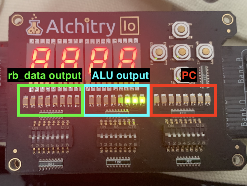
PCregister is at0x0ALUoutput is0x7- ..and
rb_dataoutput is0x0(since all registers in theREGFILEinitially contains0).
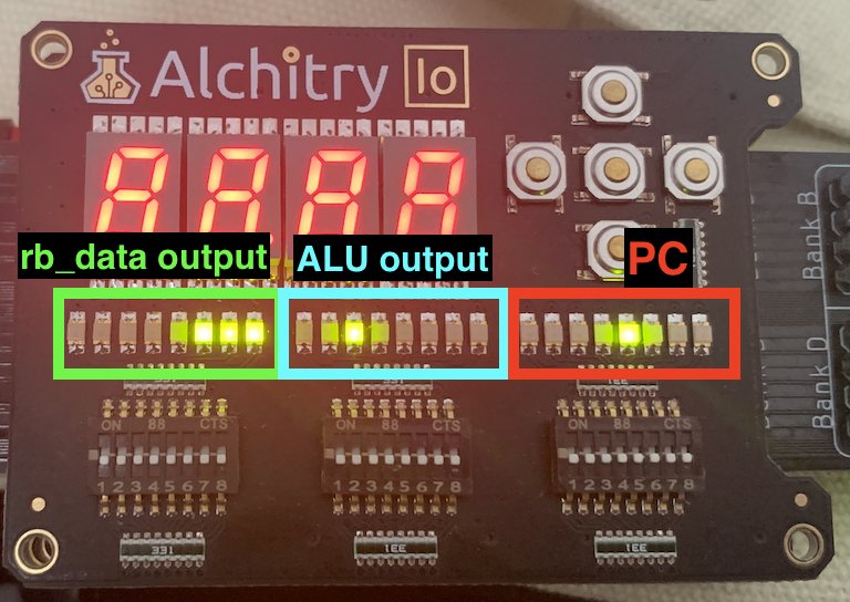
One second later, you should see this output due to instruction CMPEQ(R1, R1, R2):
PCregister is at0x4ALUoutput is0x1because comparing the same register contents should always result in a1- ..and
rb_dataoutput is0x7(showing that loading7toR1in the previous cycle is successful)
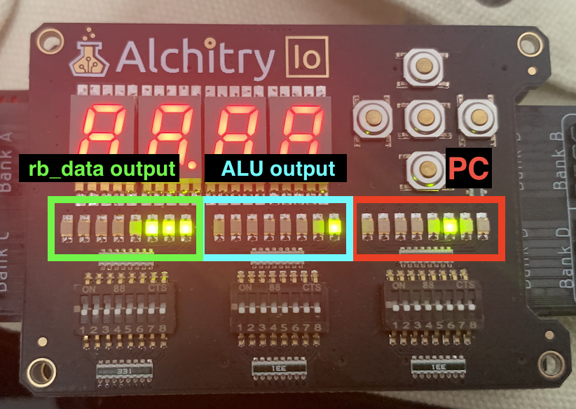
The third instruction ST(R1, 32) should result in this output:
PCregister is at0x8ALUoutput is0x20because that’s the address that we’re storing to (32in decimal)- ..and
rb_dataoutput is0x7(showing that implementation ofra2selmux is successful)
Let’s test whether the value 0x7 was properly stored to the data_memory by loading it in the next cycle with this instruction: LD(R31, 32, R3). The output that we should see is:
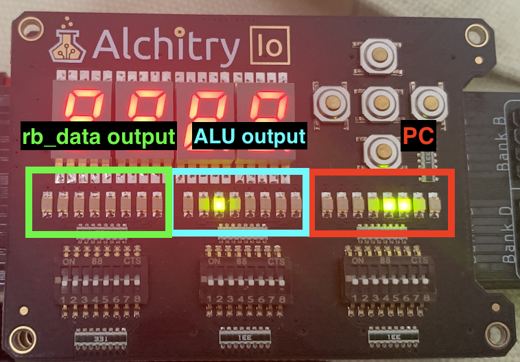
PCregister is at0xCALUoutput is0x20because that’s the address that we’re loading from (32in decimal)- ..and
rb_dataoutput is0x0(content ofR0as perinstruction[16:11])
And then perform a branch based on the content of R3: BNE(R3, 0, R1). This should result in a branch if the load was successful, as Reg[R3] will be nonzero. The output you should see is:
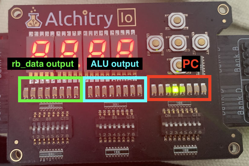
PCregister is at0x10aselis set to1duringBNE(actually it doesnt matter whataselis) and this routesPC+4+4*SXT(c)toALU’s output. The effective “target” address ifBNEis successful is0and thereforeALUoutput that shows0above is correct- ..and
rb_dataoutput is0x0(content ofR0as perinstruction[16:11])
You can try running other series of instruction to test whether other parts of the beta implemented is correct, e.g: illop triggering instructions to check if wasel mux is correctly implemented, JMP related instructions, etc.
Summary
As mentioned in the introduction, the completed project can be found here. You can carefully craft some instruction sequences to check if certain parts of the beta is correctly implemented or not.
Below are some things that each instruction in the sample above are testing:
ADDC(R31, 7, R1),CMPEQ(R1, R1, R2):- Tests if all related control signals like
wdsel,aselandbselsignals foropcoperations are correctly produced, and each muxes are correctly connected. - Tests if writing to
REGFILEis successful.
- Tests if all related control signals like
-
ST(R1, 32),LD(R31, 32, R3): tests if read and write to thedata_memorysection in externalmemory_unitis successful. BNE(R3, 0, R1): tests if branching can be done, and thecontrol_unitprocesseszproperly.
There certainly still some things that can be improved in the sample project to minimise the number of logic cells required. If you have some spare time you can try to implement beta with lesser number of logic cells, or clean up the code (eliminate some unused I/O terminal, etc). You can also try to design similar general-purpose programmable datapath for your 1D project, and run it with a series of instruction instead of hardcoding it with an fsm (but if you do choose the latter its alright as well, no penalty imposed).