 Computation Structures
50.002 Computation Structures
Information Systems Technology and Design
Singapore University of Technology and Design
Natalie Agus (Fall 2020)
Getting Started with FPGA: Part 1
This document is written to guide you with hardware coding in Lucid, a more human friendly version of Verilog – the popular but relatively difficult hardware descriptive language. Ultimately, we want to compile our code into a binary file to be loaded to our FPGA: the Alchitry Au, so that the FPGA can emulate the behavior of the machine that we describe via the code.
Some fun facts about Alchitry Au:
- It features Xilinx Artix 7 FPGA, containing 33280 logic cells (the more cells, the better. Our code can “program” these cells, so if our FPGA has more cells it means that we can implement more complex functionalities)
- On-board clock speed: 100 MHz.
- 102 IO pins (you’ll never run out of any!)
More information about the board can be found here but for now the above suffices.
It is also recommended that you read this guide at the end of week 2, after you have finished logic synthesis, otherwise you might feel a little lost.
Before you begin, please do:
- Prepare at least 50GB of free space. It goes without saying that you can use cloud storage (Dropbox, GDrive, iCloud Drive, AWS Cloud) or get an external drive.
If you’re a MacOS user, then you’d need to install Windows (dual-boot with Bootcamp is recommended, update your OS to the latest version first). You need at least 60-70 GB for this, since Windows OS alone will take up to 20GB of your space. If needed, see this step-by-step guide on how to perform bootcamp.
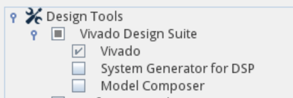
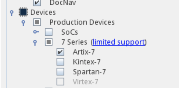
- Install Xilinx Vivado : scroll down until you see the Self-extracting Web-Installer (Windows or Linux only). Sorry Mac users, you will have to Bootcamp Windows 10 / Ubuntu.
- Sign-up for a free Xilinx account
- Then, when you obtain the installer, install the Vivado HL WebPACK Edition (this is the free edition)
- To avoid installing too many things, select just Vivado and Artix7:
- Install Java SE (Java JDK & JRE included in it), although it is likely that you already have these installed due to your other subject.
- Then, download the Alchitry Lab IDE. This is the IDE where you can write your program in Lucid and flash it to the FPGA via USB connection.
If needed, see step by step installation here.
By the end of this document, you should be able to create simple combinational logic modules and test them on Alchitry Au.
Creating Combinational Logic Modules
The purpose of using an FPGA is so that we can have an actual hardware device that realises (actually implements) certain functions or logic that we have designed.
Let’s take an example of a Full Adder unit that we did in Lab 2:
- After drawing its schematic at first, we can then test or simulate its functionalities using jsim or some other tools.
- Then you need to actually solder a bunch of things (transistors, etc) to prove your concept. This is quite a hassle.
- If you were to design a state-of-the-art full adder unit, you will want to mass-produce your design (if it works exceptionally well).
Alternatively, we can use an FPGA to prove our concept. You can load your program (describing how your Full Adder works) onto an FPGA, and now the FPGA can be an actual working Full Adder unit.
How can we write this module/unit in Lucid?
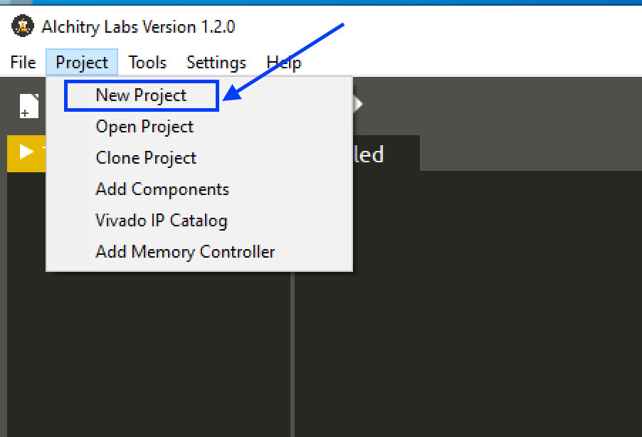
Firstly, create a project in Alchitry Lab,
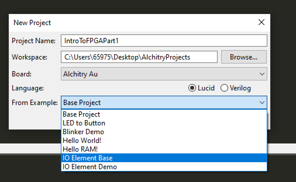
Give it some name, ensure that it is Au and Lucid. Also, use the IO Element Base template. It sets the IO Unit for you:
Now you should see that you have a project with several files:
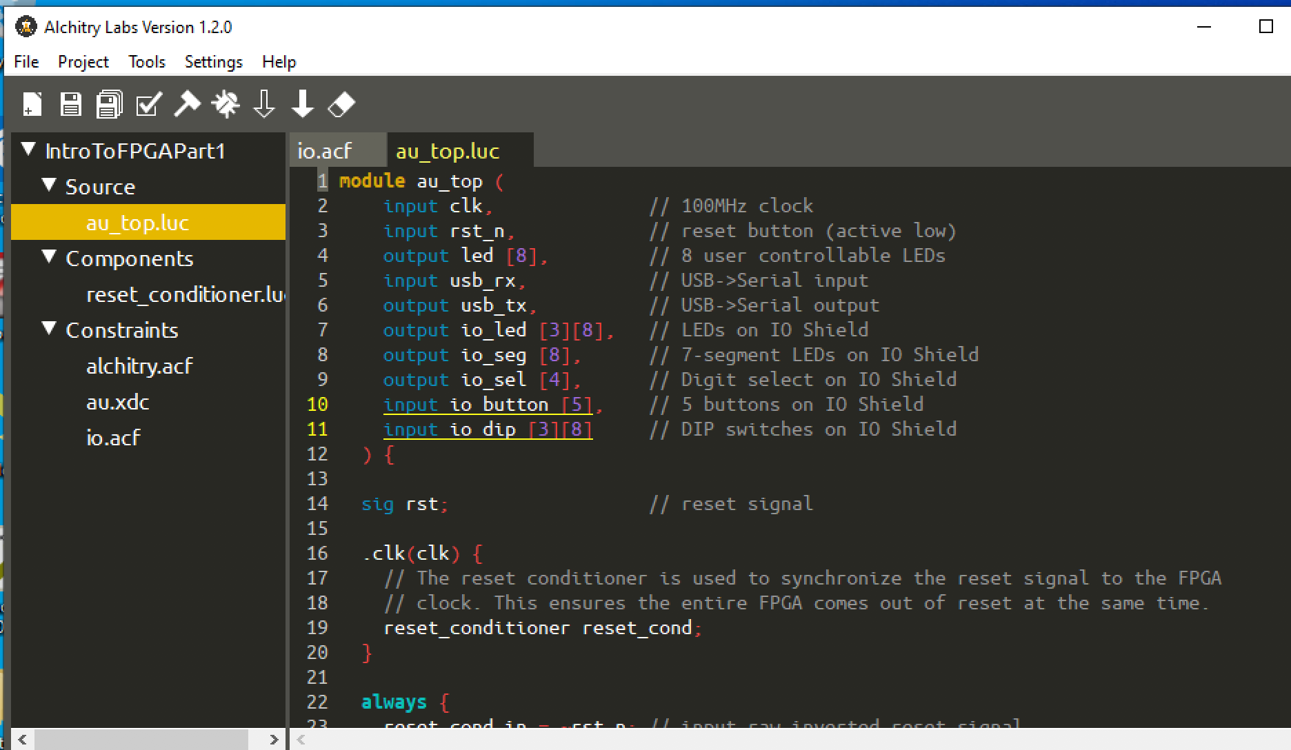
You need to do your own self-study part to fill in the gaps and understand how the code works better by reading the tutorials provided by the original developer. The course handout also provides you some useful self-study materials. This document is only made to complement and speed up your self-study process, but it doesn’t mean that you can forget about reading anything else.
If you haven’t read any tutorials about Lucid and Alchitry yet, here’s some quick information:
-
Under
Source, thats where you will write all your script.alu.lucis like themainscript, so do not delete that. alu.lucis the only script that can interface with external input and output, like LED, switches and buttons.- Each
.lucscript should describe a component (combinational / sequential). - Typically in
alu.lucwe combine all components together with input/output, forming a whole complete device. - Under
Componentsis where you can add standard components (like standard library modules). Right click on it and clickAdd Components, and you’ll be faced with a phethora of modules which you may or may not use depending on your application: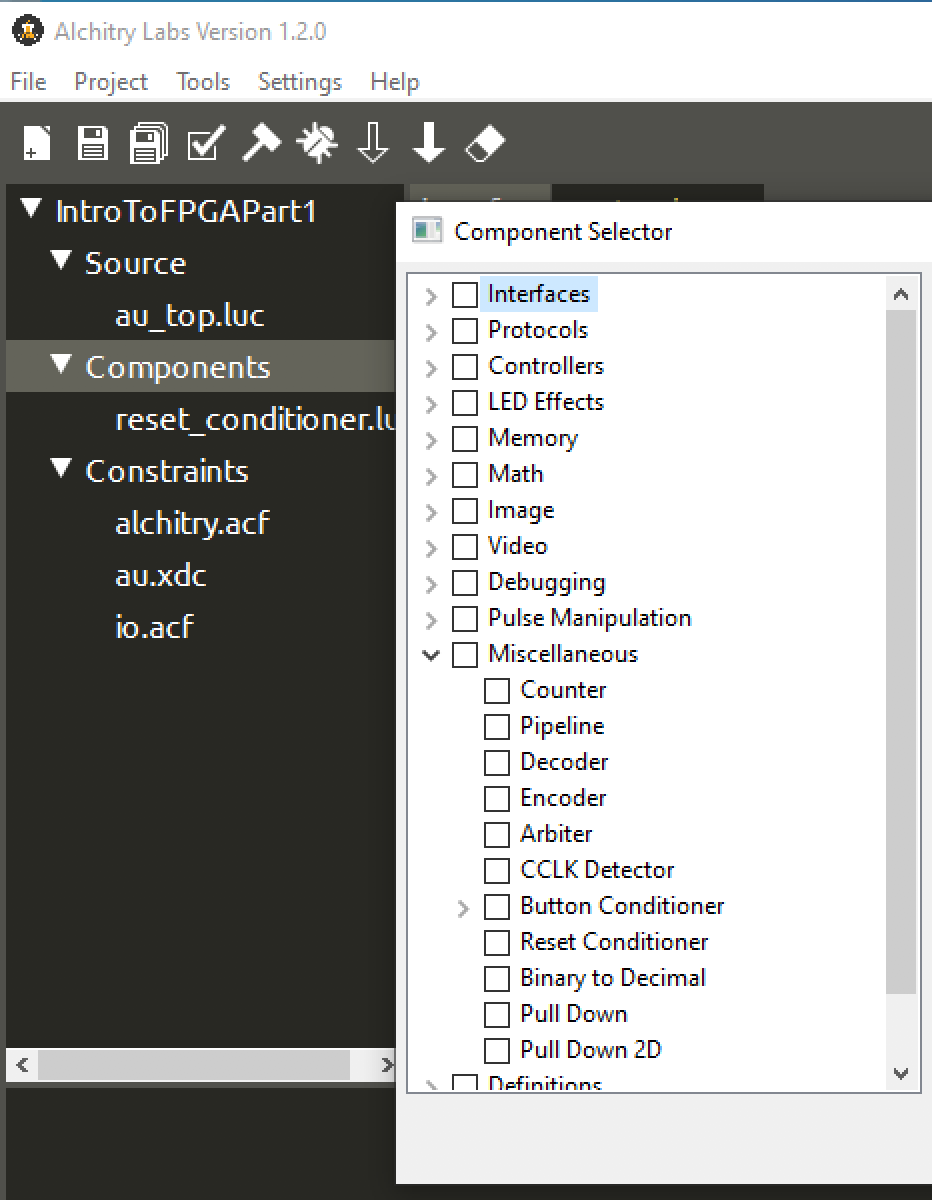
But a few important ones that you probably can’t live without are: counter, edge detector, button conditioner. We will meet them soon. - Under
Constraintsis where you can define your input and output terminals. We will come back to this later.
So now back to creating a Full Adder. By now you should know that this circuit implements a full adder functionality:
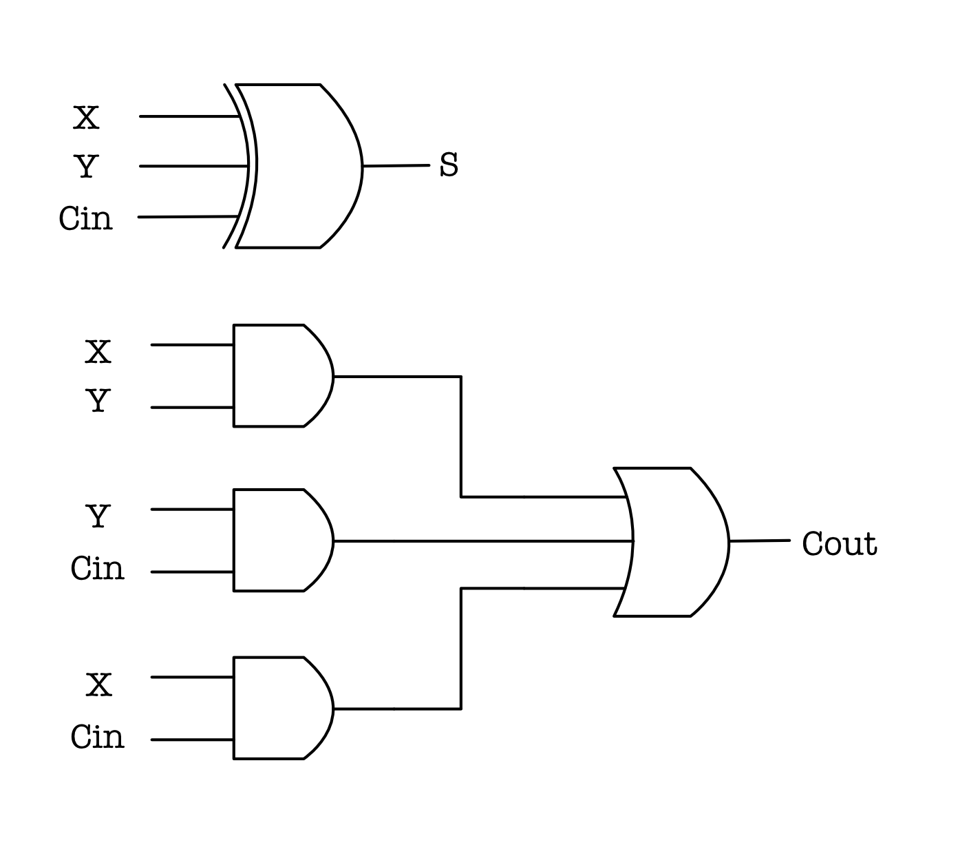
We can describe this schematic in Lucid, by first defining the input and output.
Define Input and Output terminals
Create a new source file and name it full_adder.luc. You will see that all lucid files should begin with terminals definition. In a full adder, we have 3 1-bit inputs: x, y, cin and 2 1-bit outputs: s, cout . Therefore we shall modify the header as such:
module full_adder (
	input x,
	input y,
	input cin,
	output s,
	output cout
)
Since FA is a combinational logic device, then we don’t have to use the CLK.
And then in the body, we have the always block, which as the name suggests it signifies a connection, something that is always connected.
Remember that in this block we are describing how a hardware device should behave, that is: literally describing its schematic in terms of code for Alchitry / Vivado to interpret and create an appropriate hardware description for the Au board to run.
Above the always block we can define other modules to be used, clock or reset signals, or simply intermediary connections using the keyword sig.
The following code describes the schematic of an FA. The syntax is self-explanatory. Refer to Page 2 of the documentation (Lucid Quick Reference Guide) for a summary of syntaxes.
{
sig i, j, k; // connector
always {
	s = x ^ y ^ cin;
	i = x & y;
	j = x & cin;
	k = y & cin;
	cout = i | j | k;
	}
}
The values on the right of the = sign is the value that you will assign to the connection name on its left.
You can download completed full_adder.luc here.
Connect Unit to I/O for Testing
Now let’s declare and connect the Full Adder module in au_top.luc so that we can supply an actual input and output to the unit. Add the following line below sig rst in au_top.luc:
sig rst; // reset signal
full_adder fulladder;
Then, connect the input and output terminal of the fulladder with some preset IO terminals in the always block, below the io_sel = 4hf line (keep the rest intact):
...
io_sel = 4hf; // select no digits

fulladder.x = io_dip[0][0];
fulladder.y = io_dip[0][1];
fulladder.cin = io_dip[0][2];

io_led[2][1] = fulladder.s;
io_led[2][0] = fulladder.cout;
Note: It is highly recommended that you do not implement any further combinational logic modules in au_top.luc. Your code has to be as modular as possible for the sake of easy debugging and development. As a good practice, the module au_top.luc should be only used to simply connect big module(s) to the input/output terminal.
Here’s a visual representation of the schematic. In other words, au_top.luc is the script that interfaces your custom modules with the board’s input and output unit:
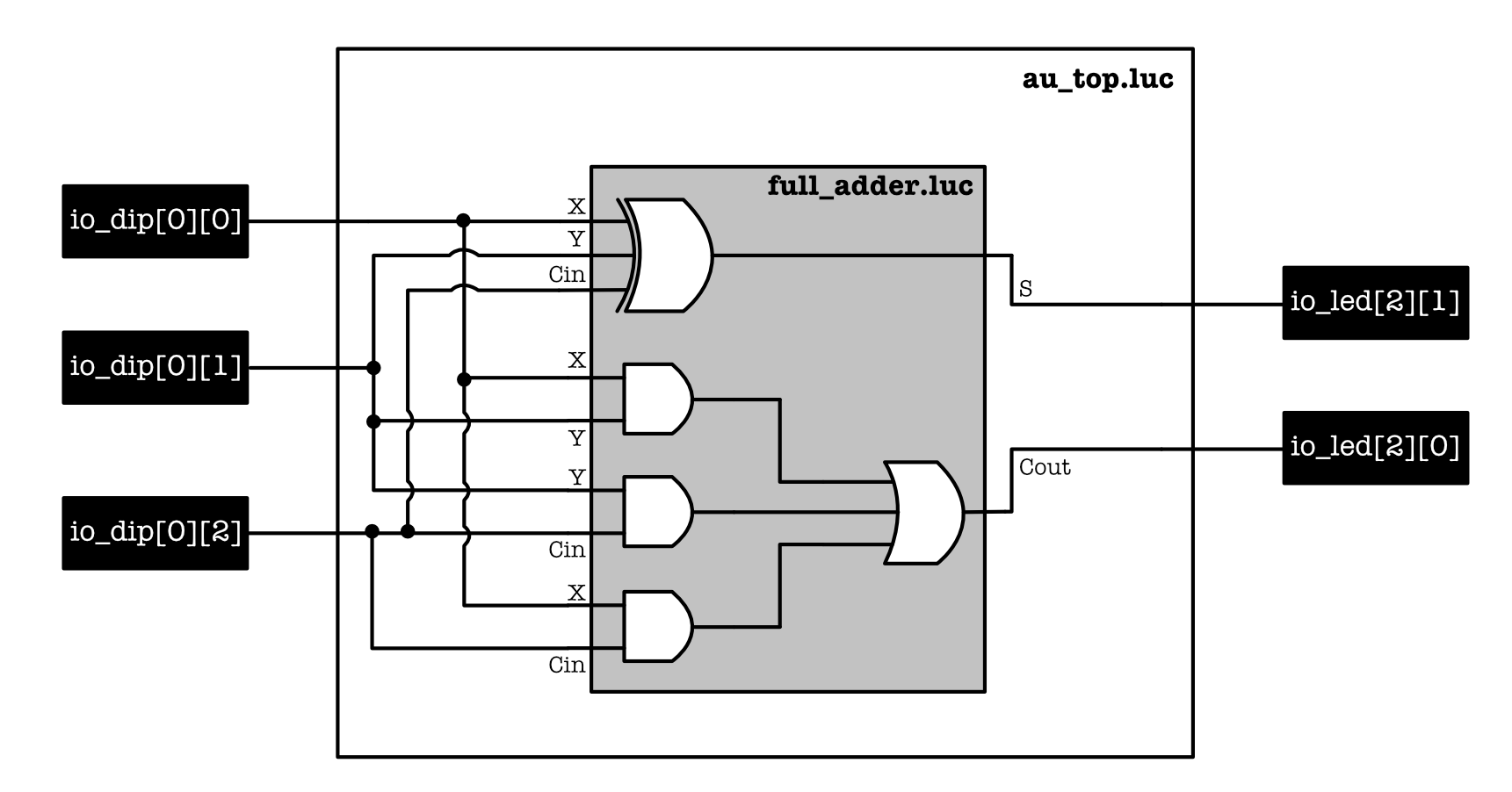
Its not as complicated as it looks, we simply want to use:
io_dip[0][0]asxio_dip[0][1]asyio_dip[0][2]ascinio_led[2][1]assio_led[2][0]ascout
Where are these stuffs on Alchitry Io? See below:
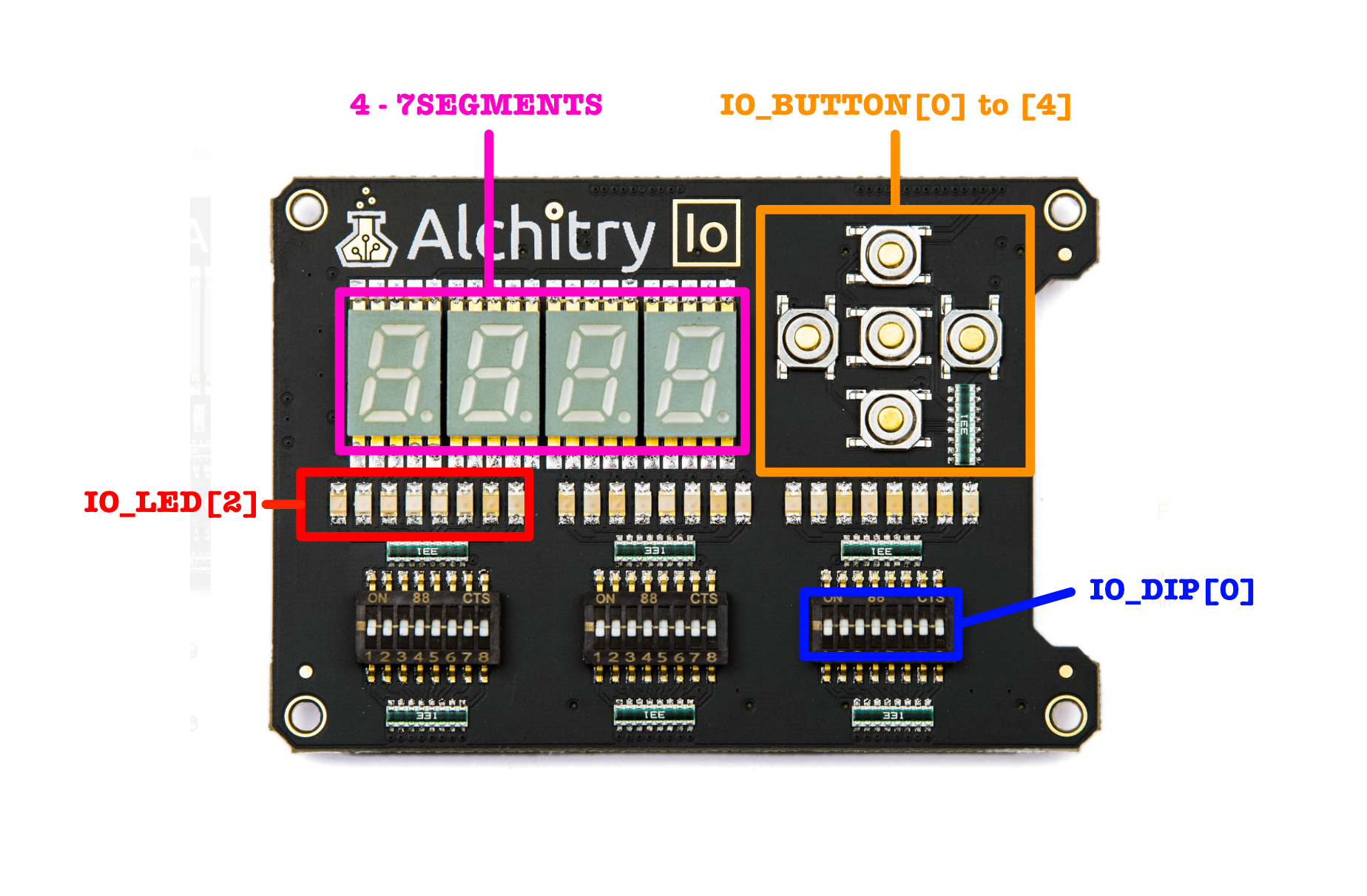
Therefore can use the dips (switch up for 1 and down for 0) to supply various combinations of input x,y,cin and observe the output at the two rightmost LED in IO_LED[2].
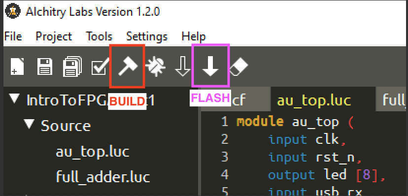
Now build your code (it may take awhile, 2-3 minutes depending on your computer stats), and flash it to the Alchitry Au:
After it is successfully loaded:
- Try using the dip switch (three rightmost of
io_dip[0]) to supply different values of input to thefulladder(all 8 combinations). - Observe the output at
io_led[2][1]andio_led[2][0]. - Convince yourself that the output conforms to the full adder’s fuctional specifications.
Alchitry Io is basically our input-output device. We use the LEDs to debug like a monitor, and buttons to supply input. yes, it is very very primitive, and it is very difficult to debug so always test each small module before integrating it!
The template Io Base already prepare these terminal namings for you, and define it under Constraints file. Open io.acf and you will see the following:
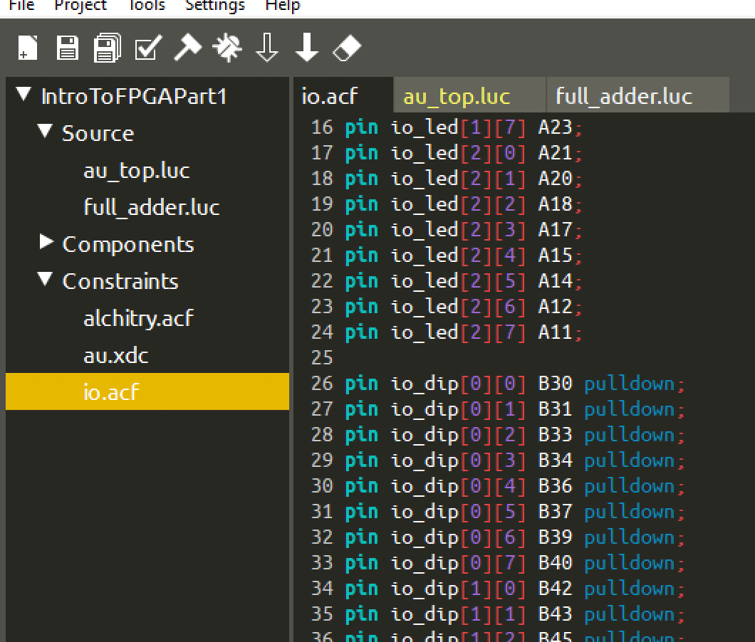
The .acf file defines input and output pins from the original schematic of Alchitry Au to its symbols to be used when we code, e.g: io_led, io_dip, etc. The ones with the keyword pulldown signifies input pins, while the rest are digital output.
An input pin with
pulldownresistor will by default give a value of0if there’s no input being supplied to prevent a floating/undefined input volrage.** It is useful to read abit about pull-down and pull-up resistors if you were to implement a unit from scratch like our Mini-Hardware Project.
This document will not teach you how to define more inputs for use on the Br board yet, or use the 7-segments to display numbers. If you’re interested to learn more, read the tutorial from the original author about Io Element
Notice how you have this part that sets the io_led to off:
Its written using the array builder, basically we set 3 sets of 8-bit values represented in hex
has 0. See Lucid Quick Reference Guide guide.
io_led = 3x{{8h00}}; // turn LEDs off
But later on we seem to overwrite two of the LED’s value to reflect s and cout:
io_led[2][1] = fulladder.s;
io_led[2][0] = fulladder.cout;
During synthesis, the setting of 0 to io_led[2][1] and io_led[2][0] is simply ignored, meaning that it wasn’t realised as a sub-circuit on the hardware. Its treated as if the assignment of these LEDs to 0 never happened.
All in all, please do not forget that:
- Anything that you write in an always block describes the behaviour (functionality) of a machine you are trying to create.
- When you click build (the hammer symbol), Xilinx Vivado and various other tools will figure out this behaviour and then create a circuit that matches this behaviour.
- This is unlike our usual Python code that is run line by line by the processor.
Building More Combinational Logic Devices
Once you have tested that your full adder works correctly, it is time to create a full-blown 8-bit ripple-carry full adder, using 8 of these units. The routine is pretty much the same. Create a file called 8_bit_full_adder.luc, and define its input/output terminals:
module eight_bit_adder (
	input x[8],
	input y[8],
	input cin,
	output s[8],
	output cout
)
Then, declare eight full adder units:
{
full_adder fulladder[8];
}
In the always block, define the connections:
{
full_adder fulladder[8];
always {
	fulladder.x = x;
	fulladder.y = y;
	fulladder.cin[0] = cin;
	fulladder.cin[7:1] = fulladder.cout[6:0];
	s = fulladder.s;
	cout = fulladder.cout[7];
	}
}
You can use the array representations to assign values in a compact way, for example:
fulladder.cin[7:1] = fulladder.cout[6:0];
is equivalent to:
fulladder.cin[7] = fulladder.cout[6];
fulladder.cin[6] = fulladder.cout[5];
fulladder.cin[5] = fulladder.cout[4];
fulladder.cin[4] = fulladder.cout[3];
fulladder.cin[3] = fulladder.cout[2];
fulladder.cin[2] = fulladder.cout[1];
fulladder.cin[1] = fulladder.cout[0];
You can download eight_bit_adder.luc here
Test with actual input/output
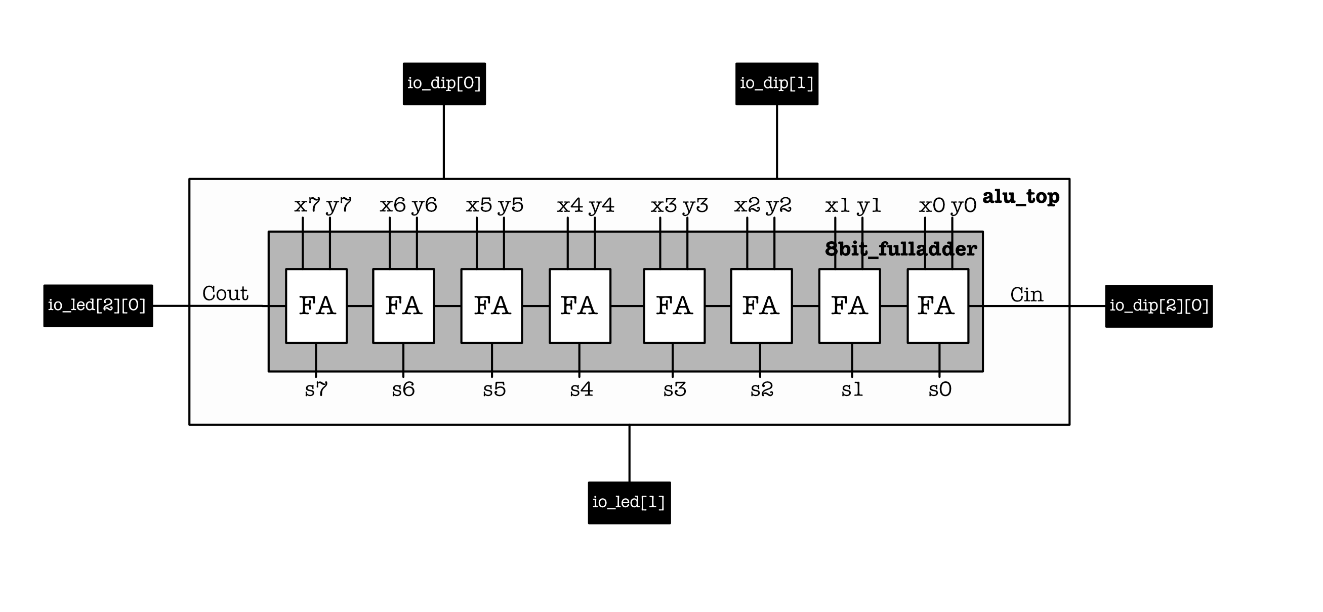
In au_top.luc, declare the 8-bit ripple carry full adder above the always block:
eight_bit_adder eightbitadder;
and connect the terminals into these IO components at the end of the always block:
eightbitadder.x = io_dip[0];
eightbitadder.y = io_dip[1];
eightbitadder.cin = io_dip[2][0];
io_led[1] = eightbitadder.s;
io_led[2][0] = eightbitadder.cout;
The simple circuit that’s described by this code is:
Build the program and flash to the Alchitry Au:
- We can use the rightmost and the middle 8
io_dipto set the8-bitxandyvalues, andio_dip[2][0]to setcin. - Observe that the output is correct, e.g: the middle 8
io_ledforsandio_led[1][0]forcoutrepresents the correct summation value.
Building ROM
Remember how we can also implement the full adder as ROM instead? Here’s how it looks like and the truth table:
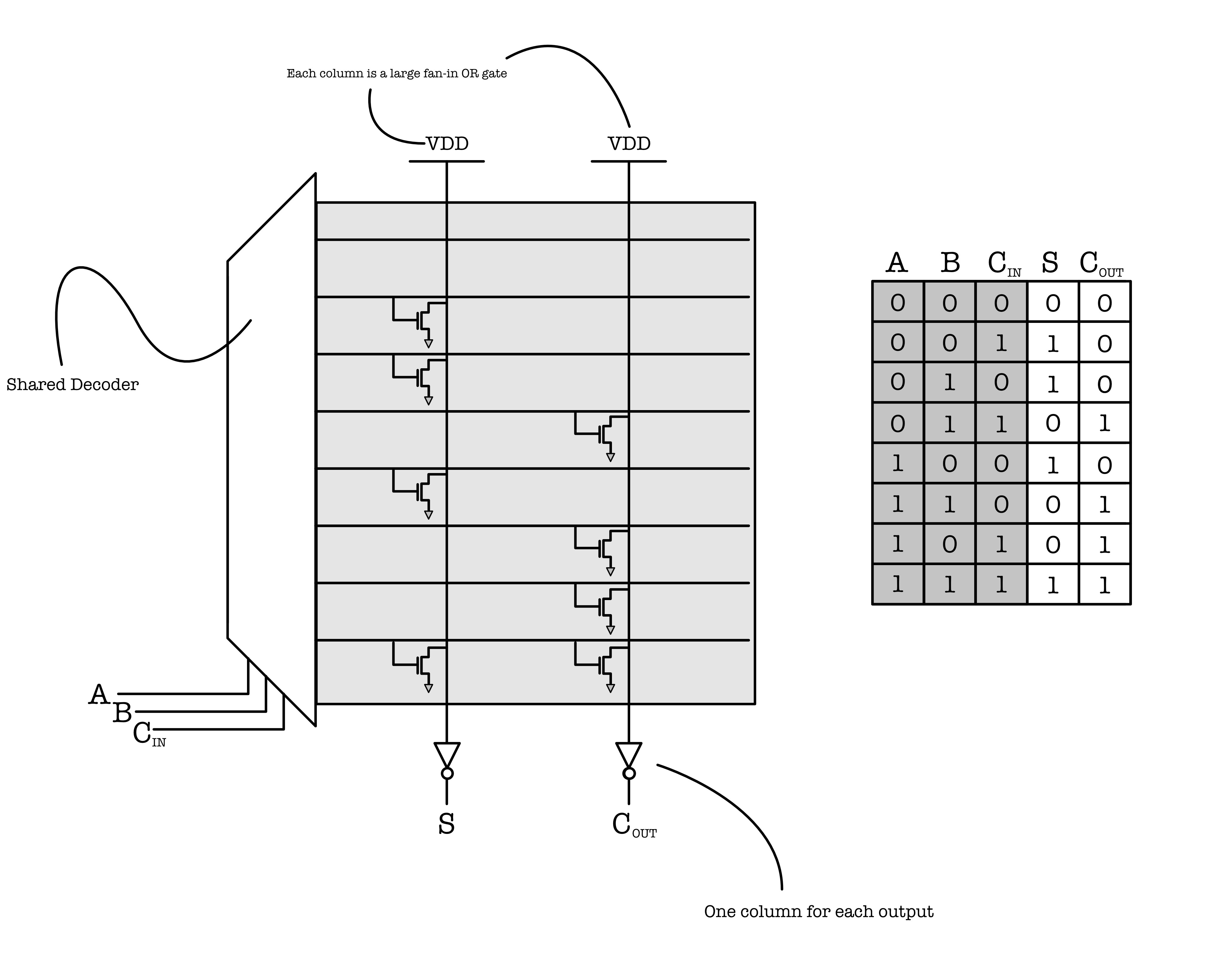
You can say that implementing anything as ROM means that we “hardcode” the answer, instead of synthesizing it using basic logic components like the gates: AND, XOR, OR, etc. The benefit of implementing the output as ROM is to minimise the hassle in synthesizing the logic out, but at the cost of space and money.
We can implement a ROM in the FPGA very easily. The following module shows an example of implementing a Full Adder as ROM:
module full_adder_ROM (
	// 3 bit input,
	// address[2] is x,
	// address[1] is y,
	// address[0] is cin
	input address[3],

	// 2 bit output,
	// value[0] is cout,
	// value[1] is s
	output value[2]
  )
{
  const FULL_ADDER = {b11, b01, b01, b10, b01, b10, b10, b00};

  always {
	value = FULL_ADDER[address];
  }
}
Notice the indexing. FULL_ADDER[000] represents the rightmost element that is b00, and so on.
Example: if address = 100, it means x=1, y=0, cin=0. This corresponds to the fifth entry (from the right) of the FULL_ADDER constant, a.k.a: our ROM. The value of FULL_ADDER[100] is 10, which means that s=1, cout=0 as per the full adder’s truth table.
You can download full_adder_ROM.luc here.
Building Multiplexer
A multiplexer can be easily implemented using the keyword case in Lucid. Consider a new combinational logic module that does left shifting with the following schematic (a, b are inputs, and s is output):
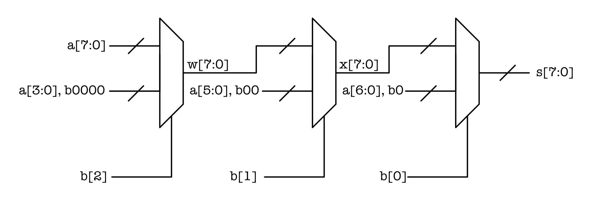
The module above can shift the 8-bit
ainput bynbits to the left wheren=0,...,7, and pad the shifted digits with zeroes. In Lab 3, you implement the -bit version of this module.
The three multiplexers can be easily implemented as follows. First, declare the input and output terminals:
module eight_bit_shiftleft (
	input a[8],
	input b[3],
	output s[8]
  )
And then declare the two 8-bit intermediary signals w and x. In the always block, we implement the three multiplexers using three case, depending on each bit of input b:
{
  sig w[8];
  sig x[8];
  always {

	case(b[2]){
        b0:
            w = a;
        b1:
            w[7:4] = a[3:0];
            w[3:0] = 4b0; // this means 4 bits of 0, equivalent to b0000
        default:
            w = a;
        }

	case(b[1]){
        b0:
            x = w;
        b1:
            x[7:2] = w[5:0];
            x[1:0] = 2b0;
        default:
            x = w;
        }

	case(b[0]){
        b0:
            s = x;
        b1:
            s[7:1] = x[6:0];
            s[0] = b0;
        default:
            s = x;
        }
  }
}
Pretty sure you’d know by now how to declare this in au_top.luc and test its funcionality.
You can download eight_bit_shiftleft.luc here.
Summary
By implementing this adder on the FPGA, we have learned:
- How to implement a combinational logic module in the
alwaysblock via boolean expression, ROM, and specify its input/output terminals clearly. - How to assemble a bigger combinational module using smaller combinational modules.
- How to test them and assemble them in
au_top.luc.
Now of course if you have read the documentation, you can simply implement an addition using a
+in Lucid without having to resort to basic boolean logic because the interpreter will implement the addition for you. Either way, the hardware circuitry is still the same.
You are highly encouraged to read this tutorial to enhance your understanding afterwards.
Important Notice about external IO:
If you would like to use external IO with the custom
Brboard, jump to this section right away and refer to this Br pins.