 Computation Structures
- Problem Set 5
- Beta Datapath
- $\beta$ Trivia (Basic)
- $\beta$ Assembly Language (Basic)
- Non $\beta$ Architecture Benchmarking (Basic)
- Clumsy Lab Assistant (Basic)
- New Beta Instruction (Basic)
- Another New Beta Instruction (Basic)
- Faulty Detection in Beta (Intermediate)
- Beta Instruction Replacements (Intermediate)
- PCSEL Fault Detection (Intermediate)
- Quality Control (Intermediate)
50.002 Computation Structures
Information Systems Technology and Design
Singapore University of Technology and Design
Problem Set 5
This page contains all practice questions that constitutes the topics learned in Week 5: Beta Datapath.
Each topic’s questions are grouped into three categories: basic, intermediate, and challenging. You are recommended to do all basic problem set before advancing further.
Beta Datapath
$\beta$ Trivia (Basic)
-
In an unpipelined Beta implementation, when is the signal
RA2SELset to1?Show AnswerThe
RA2SELsignal is set to1when executing aSTinstruction. WhenRA2SELis1the 5-bitRcfield of the instruction is sent to theRA2port of the register file, causingReg[Rc]to be sent to the write data port of main memory. -
In an unpipelined Beta implementation, when executing a
BR(foo,LP)instruction to call procedurefoo, what shouldWDSELshould be set to?Show AnswerBR(foo,LP)is a macro forBEQ(R31,foo,LP). AllBNE/BEQinstructions save the address of the following instruction in the specified destination register (LPin the example instruction). SoWDSELshould be set0, selecting the output of thePC+4logic as the data to be written into the register file. -
The minimum clock period of the unpipelined Beta implementation is determined by the propagation delays of the datapath elements and the amount of time it takes for the control signals to become valid. Which of the following select signals should become valid first in order to ensure the smallest possible clock period:
PCSEL, RA2SEL, ASEL, BSEL, WDSEL, WASEL?Show AnswerTo ensure the smallest possible clock period
RA2SELshould become valid first. TheRA2SELmux must produce a stable register address before the register file can do its thing. All other control signals affect logic that operates after the required register values have been accessed, so they don't have to be valid until later in the cycle.
$\beta$ Assembly Language (Basic)
What does the following piece of Beta assembly do? Hand assemble the beta assembly language into machine language.
I = 0x5678
B = 0x1234

LD(I,R0) -- (1)
SHLC(R0,2,R0) --  (2)
LD(R0,B,R1) -- (3)
MULC(R1,17,R1) -- (4)
ST(R1,B,R0)  -- (5)
Finally, what is the result stored in R0?
The machine language is:
I = 0x5678
B = 0x1234
|| LD(R31,I,R0) -> 011000 00000 11111 0101 0110 0111 1000
0x601F5678
|| SHLC(R0,2,R0) -> 111100 00000 00000 0000 0000 0000 0010
0xF0000002
||LD(R0,B,R1) -> 011000 00001 00000 0001 0010 0011 0100
0x60201234
||MULC(R1,17,R1) -> 110010 00001 00001 0000 0000 0001 0001
0xC8210011
||ST(R1,B,R0) -> 011001 00001 00000 0001 0010 0011 0100
0x64201234- Line 1: move the content of the memory unit at
EA=Ito registerR0 - Line 2: the content of
R0is multiplied by 4 and stored back at registerR0 - Line 3: move the content of memory address
EA:EA=B+ content of registerR0; to registerR1. - Line 4: The content of register
R1is multiplied by 17 and stored back at registerR1. - Line 5: Store / copy the content of register R1 to the memory unit with address
EA:EA=B+ content of registerR0.
R0 is the content of memory address I: Mem[I] multiplied by 4.
Non $\beta$ Architecture Benchmarking (Basic)
A local junk yard offers older CPUs with non-Beta architecture that require several clocks to execute each instruction. Here are the specifications:
\[\begin{matrix} \text{Model} & \text{Clock Rate} & \text{Avg. clocks per Instruction}\\ \hline x & 40 Mhz & 2.0\\ y & 100 Mhz & 10.0\\ z & 60 Mhz & 3.0\\ \end{matrix}\]You are going to choose the machine which will execute your benchmark program the fastest, so you compiled and ran the benchmark on the three machines and counted the total instructions executed:
-
$x$:
3,600,000instructions executed -
$y$:
1,900,000instructions executed -
$z$:
4,200,000instructions executed
Based on the above data, which machine would you choose?
First we find out the time taken to execute those instructions:
- $x$: $\frac{3.6M}{40M / 2}$ = $0.18$ seconds
- $y$: $\frac{1.9M} {100M / 10}$ = $0.19$ seconds
- $z$: $\frac{4.2M}{60M / 3}$ = $0.21$ seconds
Clumsy Lab Assistant (Basic)
Notta Kalew, a somewhat fumble-fingered lab assistant, has deleted the opcode field from the following table describing the control logic of an unpipelined Beta processor.
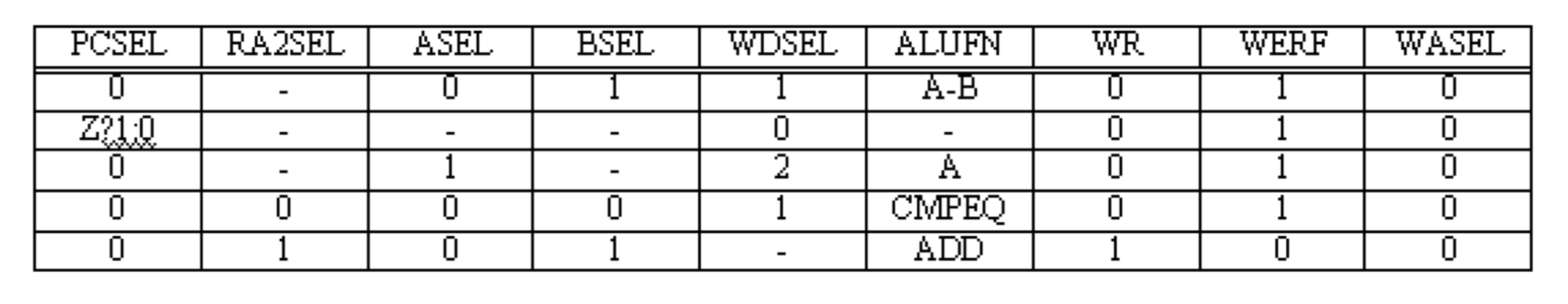
-
Help Notta out by identifying which Beta instruction is implemented by each row of the table.
Show AnswerFrom first row to the last:
SUBC, BEQ, LDR, CMPEQ, ST. -
Notta notices that
WASELis always zero in this table. Explain briefly under what circumstancesWASELwould be non-zero.Show AnswerWASELis1if aninterrupt, an illegal opcode is trapped, or a fault occurs</strong>. When WASELis1, it selectsXPas the write address for the register file;Reg[XP]is where we store the currentPC+4whenever there is an interrupt, a fault, or an illegal opcode. </p></div>
-
Notta has noticed the following C code fragment appears frequently in the benchmarks:
 int *_p; /_* Pointer to integer array *_/_
 _int i,j; /_* integer variables *_/_

 _..._

 _j = p[i]; /_* access ith element of array */
The pointer variable
pcontains the address of a dynamically allocated array of integers. The value ofp[i]is stored at the addressMem[p +4i]wherepandiare locations containing the values of the corresponding C variables. On a conventional Beta this code fragment is translated to the following instruction sequence:LD(...,R1) /* R1 contains p, the array base address */ LD(...,R2) /* R2 contains I, the array index */ ... SHLC(R2,2,R0) /* compute byte-addressed offset = 4*i */ ADD(R1,R0,R0) /* address of indexed element */ LD(R0,0,R3) /* fetch p[i] into R3 */Notta proposes the addition of an
LDXinstruction that shortens the last three instructions to:SHLC(R2,2,R0) /* compute byte-addressed offset = 4*i */ LDX(R0,R1,R3) /* fetch p[i] into R3 */Give a register-transfer language description for the
LDXinstruction.Show AnswerLDX( Ra, Rb, Rc ): EA <- Reg[Ra] + Reg[Rb] Reg[Rc] <- Mem[EA] PC <- PC + 4 -
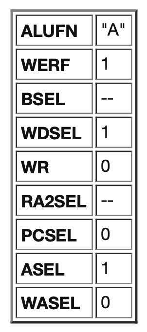
Using a table like the one above specify the control signals for the LDX opcode.
Show Answer$$\begin{matrix} PCSEL & RA2SEL & ASEL & BSEL& WDSEL & ALUFN & WR & WERF & WASEL \\ \hline 0 & 0 & 0 & 0 & 2 & ADD & 0 & 1 & 0 \end{matrix}$$
-
It occurs to Notta that adding an
STXinstruction would probably be useful too. Using this new instruction,p[i] = jmight compile into the following instruction sequence:SHLC(R2,2,R0) /* compute byte-addressed offset = 4*i */ STX(R3,R0,R1) /* R3 contains j, R1 contains p */Briefly describe what (hardware) modifications to the Beta datapath would be necessary to be able to execute
STXin a single cycle.Show AnswerThe register transfer language description of
STXwould be:
It's evident that we need to perform 3 register reads, but the Beta's register file has only 2 read ports. Thus we need to add a third read port to the register file.STX(Rc, Rb, Ra) EA <- Reg[Ra] + Reg[Rb] Mem[EA] <- Reg[Rc] PC <- PC + 4
Incidentally, adding a third read port would eliminate the need for theRA2SELmux because we no longer need to choose betweenRbandRc, since each register field has its own read port.
New Beta Instruction (Basic)
-
Write the register transfer language below corresponds to the instruction with the following control signal:
 Show Answer
Reg[Rc] <-- (PC+4)+4*SXT(C) PC <-- PC + 4 -
Explain why the following instruction cannot be added to our Beta instruction set without further hardware modifications on the datapath:
 PUSH(Rc, 4, Ra):
     Mem[Reg[Ra]] <-- Reg[Rc]
     Reg[Ra] <-- Reg[Ra] + 4
Show AnswerTo implement this
</ins>PUSH, somehow theALUwould have to produce two 32-bit values instead of the original one 32-bit output. The new two 32-bit values are:Reg[Ra]to be used as the memory address andReg[Ra]+4to be written into the register file.
Another New Beta Instruction (Basic)
Given the following C-code:
if (a != 0){
	b = 3;
}
(other code....)
where a, b are variables that have been initialised in the earlier part of the code (not shown). If we were to implement the following C-code using the Beta instruction set, we must do this in at least two cycles:
BEQ(Ra, label_continue, R31)
ADDC(R31, 3, Rb)
label_continue: (other code)
where Ra, Rb are assumed to be registers containing values a and b.
The ALU in this particular Beta however, implements five new functions on top of the standard functions: “B”, “NOTA”, “NOTB”, “TRUE”, “FALSE”.
Due to this, your classmate suggested that we can actually do this in one cycle by modifying the Control Unit to accept this new instruction called MCNZ (move constant if not zero) instead:
MCNZ(Ra, literal, Rc) :
	if(Reg[Ra] != 0)
		Reg[Rc] <-- literal
	PC <-- PC + 4
What values should the Control Unit give for this instruction MCNZ?
$$\begin{matrix}
PCSEL & RA2SEL & ASEL & BSEL& WDSEL & ALUFN & WR & WERF & WASEL \\
\hline
0 & - & - & 1 & 1 & "B" & 0 & Z?0:1 & 0 \end{matrix}$$
Note: Z?0:1 -- means 0 if Z==1, and 1 otherwise.
Faulty Detection in Beta (Intermediate)
You suspected that your Beta CPU is faulty, in particular, these two components:
- The
ASELmux might be faulty:- if
ASEL = 0, the output is always 0. - There’s no problem if
ASEL = 1.
- if
- The part of the
CUthat gives outRA2SELsignal might be faulty:RA2SELis always stuck at0(it cannot be1regardless of the instruction)
Your friend came up with several short test programs. You want to select one of these programs to run in the faulty Beta, but you don’t want to waste your time loading and running multiple programs and would like to select one that can detect both faults. Which of the following program(s) can detect both faults?
Meaning that :
-
The values in the
PC/ Registers in Regfile / Memory Unit will be different from a working Beta CPU if these programs were to be executed in this faulty Beta. -
You can be 100% sure the discrepancy is caused by both
RA2SELsignal orASELmux faulty. -
Programs that can only detect the
RA2SELsignal faulty but notASELmultiplexer faulty (or vice versa) is not acceptable.
You can assume that the initial content of all registers are 0.
Program 1:
.=0x000
LDR(constant, R0)
LDR(constant + 4, R1)
ADD(R0, R1, R2)
ST(R2, constant + 8, R31)
HALT()

constant: LONG(8)
LONG(4)
Program 2:
.=0X000
CMOVE(5, R1)
LDR(constant, R2)
ST(R2, answer, R31)
MUL(R1, R2, R3)
HALT()

constant: LONG(0)
.=0xFFFC
answer: LONG(0)
Program 3:
.=0x000
constant: LONG(8)
LONG(4)
LDR(constant, R0)
ADD(R0, R0, R0)
ST(R0, .+8, R31)
HALT()
Program 4:
.=0x000
CMOVE(5, R0)
ST(R0, constant + 8, R31)
LDR(constant, R1)
ADD(R1, R1, R2)
HALT()

.=0xABCC
constant: LONG(8)
LONG(4)
There's only one instruction: ST that requires RA2SEL to be 1. Therefore our program must have this instruction to test against a working Beta CPU. We also must ensure that we utilize instructions that results in ASEL=0 and that the output of the ASEL mux should be nonzero in a working Beta CPU. We also need to ensure that the programs need to utilize these instructions in a way that results in a different state when run on a working Beta CPU.
Program 1 and Program 4 fulfills the criteria, and the other two don't.
For Program 1:
* The content store at R2 will be 4 instead of 12 if the ASEL mux is faulty.
- We will end up storing 8 instead of 12 to
Mem[constant + 8]ifRA2SELsignal remains0due to the faultyCU.
- The content of
R31is stored toMem[Constant+8]instead of the content ofR0. Therefore,Mem[Constant+8]is0instead of5. - The content of
R2is8instead of16.
ST and OP instructions: MUL/ADD, etc that involve the ASEL mux but if you run them with the faulty Beta and with a working Beta, the end state is either the same or different due to one of the faulties only, and therefore can't be used to detect both faulties.
Beta Instruction Replacements (Intermediate)
For each of the statements below, indicate whether they’re True or False and provide your reasoning.
-
Statement 1: In the Beta, every
ADDCinstruction can always be replaced by aSUBCinstruction that puts precisely the same value in the destination register. For example,ADDC(R0,1,R0)is equal toSUBC(R0,-1,R0)(think about all constants). -
Statement 2: In a Beta program, you can use
BEQ(R31, label, R31)as a substitute forJMP(Ra)whereRastores the address oflabel, no matter wherelabelis. -
Statement 3: We can never perform
LDandSTto any two independent addresses in a single cycle (even if the memory unit supports it) by just modifying the control unit of the Beta. In other words, we need to modify the datapath of the Beta in order to do this.
Statement 1 is False. We can have ADDC(R0, -65536, R0) but we cant have SUBC(R0, 65536, R0) as the most positive number that a signed 16-bit can represent is 65535.
Statement 2 is False. Ra contains 32-bit of data, so we can set PC to be pointing to any address in the memory (4GB of address space) with JMP(Ra). However, BEQ only covers 65536*4 (above PC+4) + 65535*4 (*below and inclusive of PC+4*) bytes of address space.
Statement 3 is True. The output of the ALU supplies a single address for both load and store to the memory unit.
PCSEL Fault Detection (Intermediate)
This time round, consider a Beta machine with a faulty control unit, where its PCSEL signal is always 0, meaning that the input to the PC register is always
PC+4 regardless of the instruction.
As always, we can detect this particular fault by running a simple test program written in Beta assembly language. State which of the following programs can detect this particular fault, meaning that if it was to be run on a faulty Beta machine, we will get different results (contents) on the registers in the regfiles, PC, or Memory Unit, and provide your reasoning.
Assume that all register values were 0 at the beginning of each program execution.
Program 1: (executed for two CLK cycles)
.= 0
BEQ(R0, .+4, R31)
ADDC(R0, 1, R0)
Program 2: (executed for three CLK cycles)
.=0
CMPEQ(R0, R0, R0)
BNE(R0, .-4, R31)
ADDC(R0, 1, R0)
Program 3: (executed for four CLK cycles)
.=0
LD(R0, 0, R0)
MULC(R0, 1, R0)
BNE(R0, .+4, R31)
CMPEQ(R0, R31, R2)
Program 4: (executed for two CLK cycles)
.=0
ST(R0, x, R31)
x: LONG(12)
Program 5: (executed for two CLK cycles)
.=0
JMP(R1)
ADDC(R0, 1, R1)
Program 6: (executed for two CLK cycles)
.=0
LDR(R31, .+8, R0)
ADDC(R0, 1, R1)
x : LONG(3)
Program 2, 4, and 5 can successfully detect this faulty. All of them forces the control unit to produce non-zero PCSEL. For example, Program 4 results in illop when the Beta attempts to execute LONG(12) because it isn't an instruction. Therefore PCSEL=3 if the control unit works properly and that the content of PC will be ILLOP (wherever the address of illegal operation handler is) instead of address 0xC.
Quality Control (Intermediate)
One Beta manufacturer is having quality-control problems with their design. In particular, they’ve had reliability issues with various device connections that are circled in the diagram below.
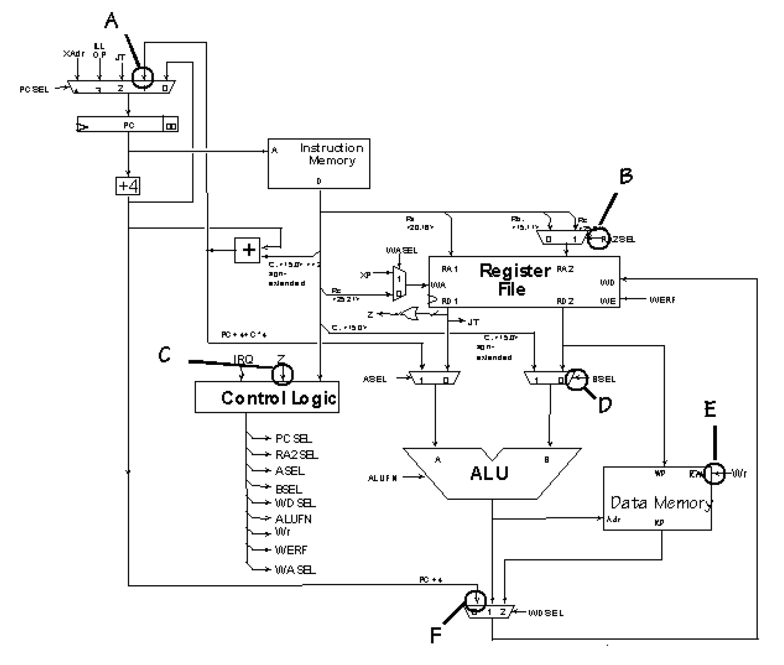
Your job is to write some test programs to help determine if a machine is fault-free. ==Assume that when a device connection is “faulty,” the indicated bus or signal is always producing “0” instead of the expected value.==
For each of the circled connections, write an instruction sequence that when executed for a specified number of cycles will leave the following result in R0:
1inR0if the connection was working.- Other values in
R0if the connection was faulty.
You can assume that all registers are reliably set to 0 before each sequence is executed.
Give your instruction sequence for each of the six indicated faults and briefly explain how each sequence detects the fault and produces something besides 1 in R0 when the fault is present:
- Fault A: Input 1 of
PCSELmux has a value of0instead ofPC+4+4*SEXT(C). - Fault B:
RA2SELmultiplexer control signal is0instead of as per intended current instructionOPCODE. - Fault C:
Zinput to control logic is always0instead of the correct value depending onRD1. - Fault D:
BSELmultiplexer control signal0instead of as per intended current instructionOPCODE. - Fault E:
WRmemory control signal is0instead of as per intended current instructionOPCODE. - Fault F: Input 0 of
WDSELmux has a value of0instead ofPC+4.
Note: there’s many alternate answers. They aren’t unique.
Fault A: Input 1 of PCSEL mux has a value of 0 instead of PC+4+4*SEXT(C).
| starts at address 0
. = 0
BEQ(R0,.+4,R31) | 0x0
ADDC(R0,1,R0) | 0x4
Execute for 2 cycles (i.e., execute two instructions):
- If fault A is not present,
R0contains1after the second cycle, since the second instruction is fetched from location0x4. - If fault A is present, the second instruction is fetched from location
0(instead of4, since the input1to thePCSELmux is0), so the value ofR0stays0. </ul>
Note that the label.+4means “memory location of current instruction + 4”, which is0+4here. </p></div>
**Fault B:** `RA2SEL` multiplexer control signal is `0` instead of as per intended current instruction `OPCODE`.Show Answer
Execute for 3 cycles:| starts at address 0 . = 0 ADDC(R1,1,R1) ST(R1,0,R0) LD(R0,0,R0)- If fault B is not present, the
STinstruction writes the value1into location0, which is thenLD-ed (loaded) intoR0. - If fault B is present, the
STinstruction writes the contents ofR0instead (ie, the value0), so now theLDinstruction puts0intoR0.
</lu></p></div> - If fault C is not present,
R0is incremented to1since the branch to memory location8is taken. - If fault C is present, the
BEQinstruction never branches, executing the instruction at location4, which leaves the contents ofR0unchanged (i.e., it's still0). - If fault D is not present,
R0is increment to1. - If fault D is present, the high-order 5-bits of the literal field (i.e., where
Rbis encoded) is used as a register address, and the contents of that register is added toR0. Since the literal is1, the second register isR0(containing0), so the value written intoR0is0.
</p></div> - If fault E is not present, the instruction writes the value
1intoMem[X], which is thenLD-ed (loaded) intoR0. - If fault E is present, the
STinstruction has no effect, so now theLDinstruction loads the original value of locationXintoR0. - If fault F is not present, the
BEQinstruction loads4intoR1and theSUBCloads1intoR0. - If fault F is present, the
BEQinstruction loads0intoR1and theSUBCloads -3 intoR0.
**Fault C:** `Z` input to control logic is always `0` instead of the correct value depending on `RD1`.Show Answer
Execute for 2 cycles:| starts at address 0 . = 0 BEQ(R0,.+8,R31) ADDC(R0,0,R0) ADDC(R0,1,R0)
**Fault D:** `BSEL` multiplexer control signal `0` instead of as per intended current instruction `OPCODE`.Show Answer
Execute for 1 cycle:| starts at address 0 . = 0 ADDC(R0,1,R0)
**Fault E:** `WR` memory control signal is `0` instead of as per intended current instruction `OPCODE`.Show Answer
Execute for 3 cycles:| starts at address 0 . = 0 ADDC(R1,1,R1) ST(R1,X,R31) LD(R31,X,R0) . = 0x100 X: LONG(0)Show Answer
Execute for 2 cycles:| starts at address 0 . = 0 BEQ(R0,.+4,R1) SUBC(R1,3,R0)
- If fault B is not present, the