 Computation Structures
50.002 Computation Structures
Information Systems Technology and Design
Singapore University of Technology and Design
Problem Set 3
This page contains all practice questions that constitutes the topics learned in Week 3: Sequential Logic and Synchronization and FSM.
Each topic’s questions are grouped into three categories: basic, intermediate, and challenging. You are recommended to do all basic problem set before advancing further.
Sequential Logic and Synchronization
You can refer to the notes here if you need to revise.
Warm-up Timing Computations (Basic)
Consider the following diagram of a simple sequential circuit:
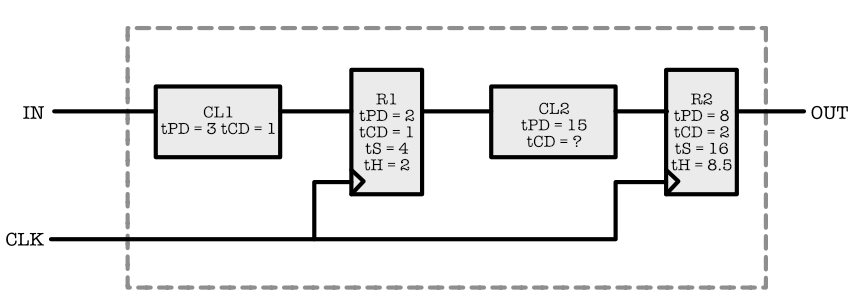
The components labeled CL1 and CL2 are combinational; R1 and R2 are edge triggered flip flops. Timing parameters for each component are as noted. Answer both questions below:
-
Suggest the values for each timing specifications ($t_S$, $t_H$, $t_{CD}$ , $t_{CD}$ CL2, $t_{PD}$, $t_{CLK}$ – clock period) for the system as a whole using the timing specifications of each of the internal components that are given in the figure.
Show Answer$t_H$ and $t_S$ is for IN, $t_{CD}$ and $t_{PD}$ is for CLK. Below are the proposed values: $$ \begin{aligned} t_S &= t_{S.R1} + t_{PD.CL1} = 4 + 3 = 7\\ t_H &= t_{H.R1} - t_{CD.CL1} = 2 - 1 = 1\\ t_{CD} \text{ CL2} &=t_{H.R2} - t_{CD.R1} = 7.5\\ t_{CD} &= t_{CD.R2} = 2\\ t_{PD} &= t_{PD.R2} = 8\\ t_{CLK} &\geq t_{PD.R1} + t_{PD.CL2} + t_{S.R2} = 2 + 15 + 16 = 33 \end{aligned}$$
From this, hopefully you realise that the $t_{PD}$ and $t_{CD}$ of a sequential circuit is counted from the last downstream register(s) -- there can be more than one -- in the circuit because our reference "input" is no longer IN but the CLK.
Similarly, $t_S$ and $t_H$ is concerning the path from IN until the first upstream register(s) -- there can be more than one -- in the circuit.
The dynamic discipline is always obeyed in any middle path between two DFFs or register in the circuit because of the hardware characteristics ($t_{CD}$s and CLK period) of the sequential circuit, so we don't need to worry about that. Therefore the definition of $t_S$ and $t_H$ of the entire circuit is only concerning the first upstream register, because this is where we need need to be wary of its $t_S$ and $t_H$ since it has to be fulfilled by the (unreliable) external input. -
Suppose you had available a faster version of CL2 having a propagation delay of 3 and a contamination delay of zero. Could you substitute the faster CL2 for the one shown in the diagram Explain.
Show AnswerNo we can't. The contamination delay for R1 is 1, while the contamination delay for CL2 is 0. After CLK change, R2 input is valid and stable for 1s due to $t_{CD}$ of CL2 before turning invalid, but its $t_H$ required is 8.5s.
Timing Plot Analysis (Basic)
Consider the following unusual D-latch configuration:
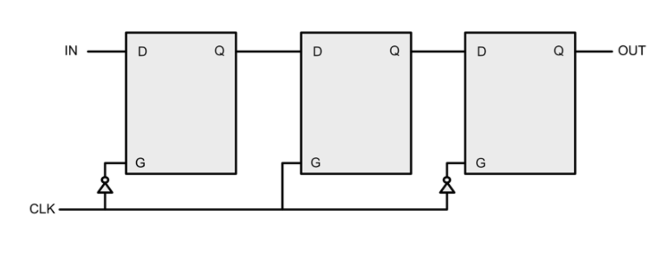
Now we feed it the following input signal and CLK signal. Which of the following signal plots represent the output of this device made out of 3 D-latches? Assume that the jagged edges means unknown value and that the contents of each latch in the beginning is unknown.
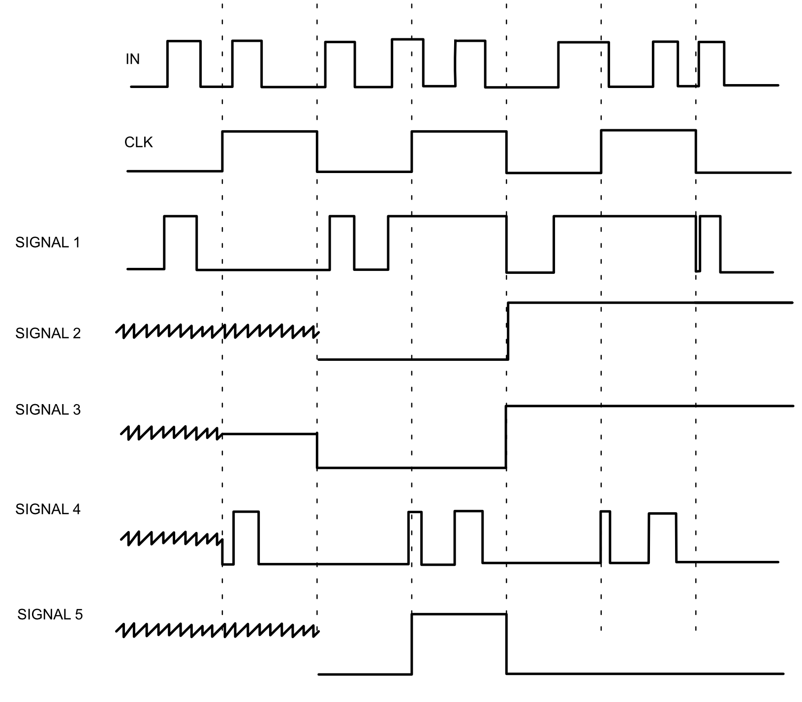
Signal 2 is the output of the device since there's two unknown outputs (it takes two half-clock cycles for the input to be propagated to the output).
Signal 5, although it has "invalid" values for two clock cycles isn't the answer because since it is an odd-numbered DFFs, it will change output at the </strong>falling</strong> edge, as opposed to rising edge in a normal DFF with two latches.
Another Timing Computations (Basic)
Consider the following circuit, and notice the feedback loop:
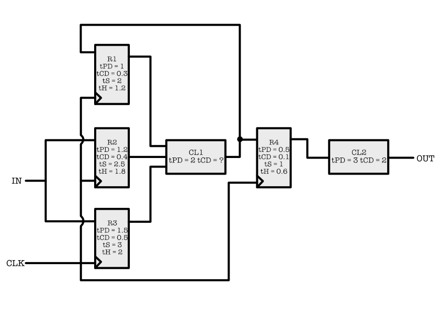
Setup time, hold time, propagation delay, and contamination delay (all in nanoseconds) of each component is as written above. Lets now analyse its timing constraints:
-
What is the minimum contamination delay ($t_{CD}$) of Combinational Logic 1 such that the sequential circuit may still function properly?
Show AnswerThe combinational logic unit 1 (CL1) is responsible for the hold times of R4 and R1. Since R1's $t_{H}$ is larger than R4, we should use that (R1's $t_{H}$) to compute min $t_{CD}$ for CL1. $t_{H}$ of R1 can be satisfied using the $t_{CD}$ of CL1 plus the $\min t_{CD}$ of either R1, R2, or R3. Hence, minimum acceptable $t_{CD}$ of CL1 is $t_{H}$ R1 - $t_{CD}$ R1 = 1.2 - 0.3 = 0.9ns.
-
Write down the minimum CLK period for the sequential circuit to function properly.
Show AnswerThe clock period must be big enough for signals to propagate from the upstream registers on the left to any downstream registers R1 or R4.
There are six paths to be considered in total where $t_2$ constraint must be obeyed in all of them: R1-CL1-R1, R1-CL1-R4, R2-CL1-R1, R2-CL1-R4, R3-CL1-R1, and R3-CL1-R4.
The longest path is formed by the $t_{PD}$ of R3 + $t_{PD}$ CL1 + $t_{S}$ R1 = 1.5 + 2 + 2 = 5.5ns. -
Write down the minimum hold time ($t_{H}$) for the IN signal to the system.
Show AnswerThe input must satisfy the $t_{H}$ of both R2 and R3, which is 2ns.
-
Write down the propagation time of the sequential logic circuit.
Show AnswerThe propagation time of the circuit is counted from R4 onwards since it is the last register in the circuit, hence it $t_{PD}$ R4 + $t_{PD}$ CL2 = 3.5ns.
Metastable State Analysis (Basic)
Consider the following D-latch device and its VTC plot:
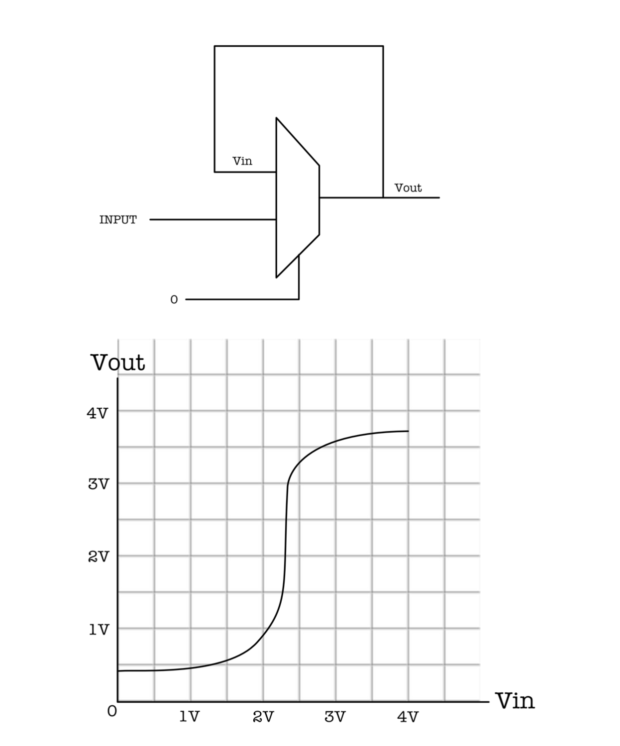
We are given the following specification about the multiplexer’s valid operating voltage ranges: $V_{IL} = 1V, V_{OL} = 0.5V, V_{IH} = 3V, V_{OH} = 3.5V$. The noise margin is $0.5V$ and we can assume that the device obeys the static discipline.
-
Which voltage value approximately, has the highest probability for the device to be in the metastable state?
Show AnswerWe plot the line $Vout == Vin$ and find the intersection with the VTC curve to be approximately at 2.35V. This is the Vin value that has the highest probability for the device to stay in metastable state.
- Compare $V_{IN} = 0.9V$ vs $V_{IN} = 3V$. Which input voltage will most likely cause the device stay in the metastable state?
Show Answer
Both input voltage values are valid inputs. Therefore the device will always produce valid output voltages since it obeys the static discipline. We can say that both values are equally unlikely to stay in the metastable state.
-
Compare $V_{IN} = 2.1V$ vs $V_{IN} = 2.5V$. Which input voltage will most likely cause the device stay in the metastable state?
Show AnswerBoth input voltage values are invalid inputs.
From the graph, we can deduce that $V_{IN} = 2.1V$ results in $V_{OUT} = 1V$, while $V_{IN} = 2.5V$ results in $V_{OUT} = 3.3V$.
Taking $2.35V$ as the most likely voltage value for the device to stay in the metastable state, $3.3V$ is nearer to $2.35V$ as opposed to $1V$. Hence, we can deduce that $V_{IN} = 2.5V$ is more likely to cause the device to stay in the metastable state.
Determining Suitable Clock Period (Intermediate)
The following circuit diagram implements a sequential circuit with two state bits, S0 and S1:
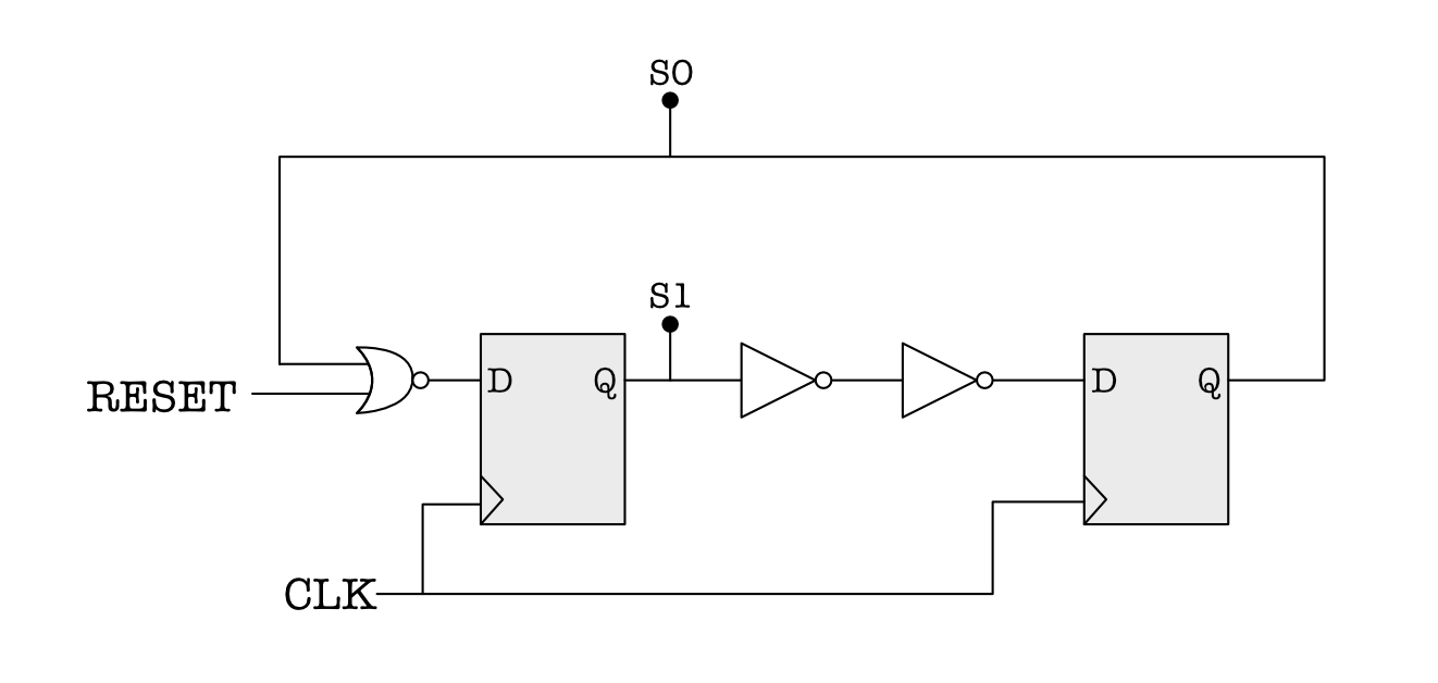
The specifications are as follows:
- $t_{PD}$, $t_{CD}$, $t_{S}$, $t_{H}$, of both registers: 0.5s, 0.3s, 1.0s, and 0.5s respectively.
- $t_{PD}$, $t_{CD}$ of inverters and NOR gates: 0.5s, and 0.4s respectively.
Answer the following questions:
-
What is the smallest clock period for which the circuit still operates correctly?
Show AnswerThere are two contraints to check:
$$\begin{aligned} t_{PD.REG} + t_{PD.INV} + t_{PD.INV} + t_{S.REG} & \leq t_{CLK}\\ t_{PD.REG} + t_{PD.NOR2} + t_{S.REG} &\leq t_{CLK} \end{aligned}$$
We need to find the largest value of $t_{CLK}$ that satisfies both constraints. This comes from the first constraint that requires $t_{CLK} \geq$ 2.5s. -
A sharp-eyed student suggests optimizing the circuit by removing the pair of inverters and connecting the Q output of the left register directly to the D input of the right register. If the clock period could be adjusted appropriately, would the optimized circuit operate correctly? If yes, explain the adjustment to the clock period will be needed.
Show AnswerNo, the circuit won't operate correctly since $t_{CD.REG} < t_{HOLD.REG}$, i.e., the output of the left register doesn't meet the required hold time when connected directly to the input of the right register.
-
When the RESET signal is set to “1” for several cycles, what values are
S0andS1set to?Show AnswerS0 = 0, S1 = 0 -
Assuming the RESET signal has been set to “0” and will stay that way, what is the state following S0=1 and S1=1?
Show AnswerS0 = 1, S1 = 0
Synchronizability (Basic)
Which of the following cannot be made to function with perfect reliability, assuming reliable components and connections? Explain your reasoning.
Some of the specifications refer to “bounded time” which means there is a specified time interval, measured from the most recent input transition, after which the output is stable and valid.
- A circuit that in unbounded time indicates which of two game show contestants pressed their button first.
Show Answer
It is possible to build this unbounded-time arbiter.
It may take an arbitrary period, after which it will produce a decision and a signal that indicates that its made a decision. - A circuit that in bounded time indicates which of two game show contestants pressed their button first.
Show Answer
This is a restatement of the "bounded time arbiter problem", known to be unsolvable in theory. In practice we can build a circuit to solve this problem where the probability of failure is related to $t_{PD}$. For "large" $t_{PD}$ (eg, 10's of nanoseconds in today's technologies) the probability of failure can be made very small (eg, 1 failure in billions of years).
- A circuit that determines if button A was pressed before a specified deadline. Assume the circuit has an accurate internal signal that transitions from 0 to 1 when the deadline is reached. The output should be 1 if the button was pressed on or before the deadline, 0 if pressed after the deadline. The output should be valid and stable within a specified $t_{PD}$.
Show Answer
This is another restatement of the "bounded time arbiter problem", known to be unsolvable in theory. Of course, given sufficiently long time bounds, we can engineer practical approximate solutions (see the answer to the previous question).
- A circuit that in bounded time indicates which of two game show contestants pressed their button first if the presses were more than 0.1 second apart, otherwise the circuit lights up a “TIE” light.
Show Answer
Not possible, same reasoning as the previous question. This circuit will suffer metastability problems because the decision as to whether the presses were 0.1 seconds apart is subject to metastability problems.
- A circuit that in bounded time indicates that at least one button has been pressed by some contestant.
Show Answer
Yes, an
ORgate will do the job. - A circuit that in bounded time indicates that exactly one of the contestants has pressed their button. You can assume there are only two contestants.
Show Answer
Yes, an
XORgate will do the job. -
A circuit that has two parts: (a). A subcircuit that indicates which of two game show contestants pressed their button first, and (b). A subcircuit that in bounded time lights a “TIE” light if the (a) subcircuit hasn’t produced an answer after 1 second. The “TIE” light should stay lit even if (a) makes a decision at some later point.
Show AnswerBoth subcircuits will suffer metastability problems. (a) is asking for an arbiter (see part 2 above) and (b) has the same difficulties as outlined for part 3 above.
-
A circuit that converts button presses from two contestants into the following two-bit output encoding. The circuit has two inputs, A and B, one for each contestant. A contestant’s input will transition from 0 to 1 when he/she presses his/her button. The final output should be:
- 00 if neither contestant is pressing their button
- 01 if contestant A is pressing her button
- 10 if contestant B is pressing her button
- 11 if both contestants are pressing their buttons
The output should be valid and stable within a specified $t_{PD}$ of the most recent input transition.
Show AnswerThe low-order bit of the encoding is the signal from A, the high-order bit is the signal from B. Nothing to go metastable here.
State Machine
You can refer to the notes here if you need to revise.
Classifying FSM (Basic)
The diagram below illustrates the FSM diagram of a machine that has the same purpose. The circle that is bolded signifies the starting state.
State whether the following is true or false and explain your answer:
- Statement 1: “Diagram A illustrates a Mealy machine.”
- Statement 2: “Diagram B can be further minimized.”
What is the purpose of these FSMs?
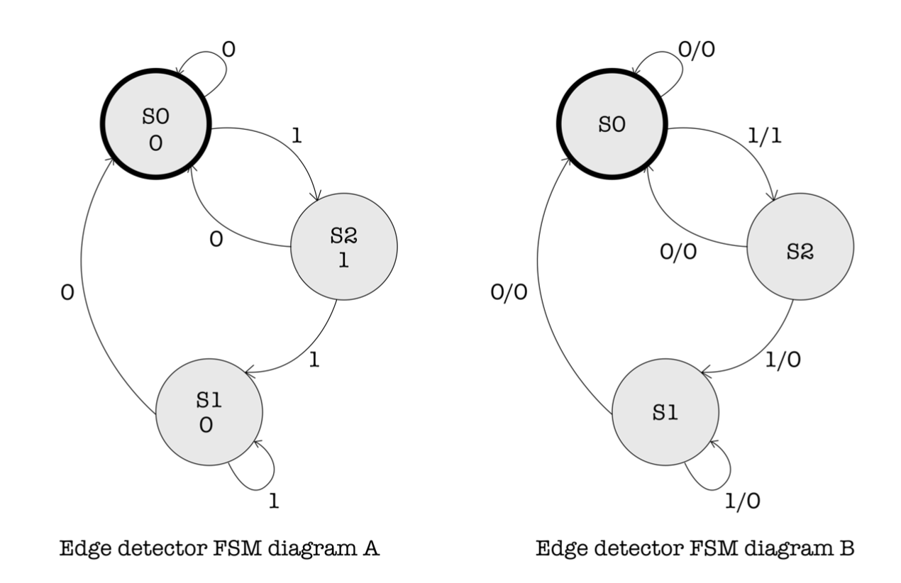
Statement 1 is false because the machine in Diagram A has its output that depends only on its state. Statement 2 is true, we can minimise it into just two states because S1 and S2 are equivalent.
The purpose of both machines is to detect the presence of an edge and output a 1 once for the cycle where the edge happens, and 0 otherwise.
Your friend plot the timing diagram of the machine in Diagram A and obtain the following output:
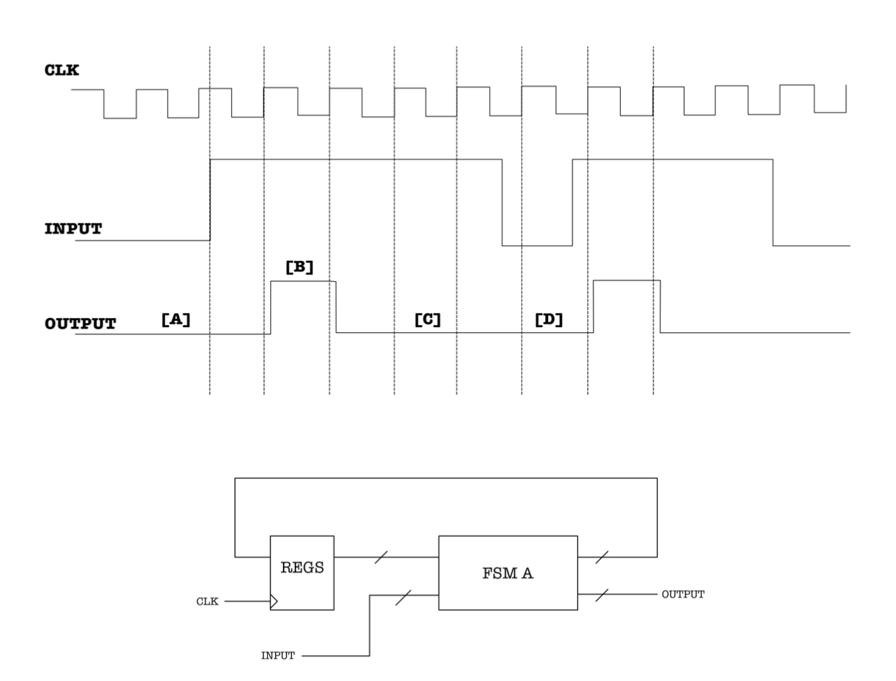
Assume that the machine starts at S0. While referring to the FSM diagram up above, write the current state that occurs at instances [A], [B], [C], and [D] respectively.
We can obtain the answers easily by running the FSM step by step. At each labeled instance, the machine is at the following states:
[A]: S0,[B]: S2,[C]: S1,[D]: S0,
An Incomplete State Machine (Basic)
The ACME Company has recently received an order from a Mr. Wiley E. Coyote for their all-digital Perfectly Perplexing Padlock:
- The P3 has two buttons (“0” and “1”) that when pressed cause the FSM controlling the lock to advance to a new state.
- In addition to advancing the FSM, each button press is encoded on the B signal (B=0 for button “0”, B=1 for button “1”).
- The padlock unlocks when the FSM sets the UNLOCK output signal to 1, which it does whenever the last N button presses correspond to the unique N-digit combination.
Unfortunately the design notes for the P3 are incomplete. Using the specification above and clues gleaned from the partially completed diagrams below fill in the information that is missing from the state transition diagram with its accompanying truth table.
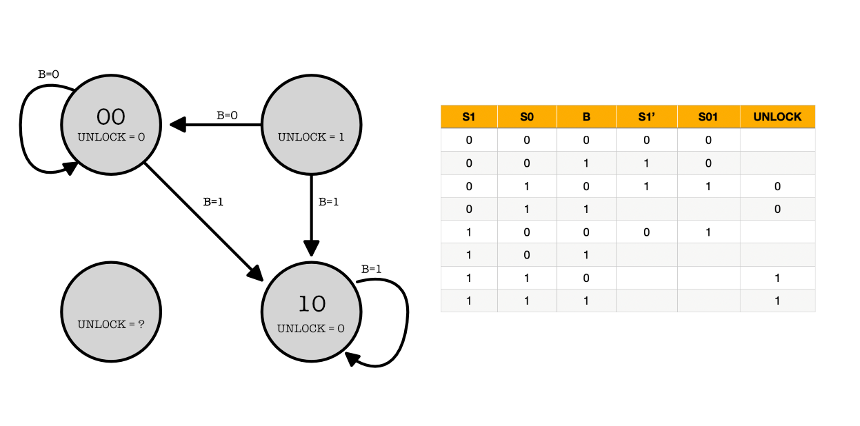
When done,
-
Each state in the transition diagram should be assigned a 2-bit state name S1S0 (note that in this design the state name is not derived from the combination that opens the lock),
-
The arcs leaving each state should be mutually exclusive and collectively exhaustive,
-
The value for UNLOCK should be specified for each state, and o the truth table should be completed.
Also, what is the combination of the lock?
This state machine is a Moore machine. The completed state transition diagram and truth table is as follows:
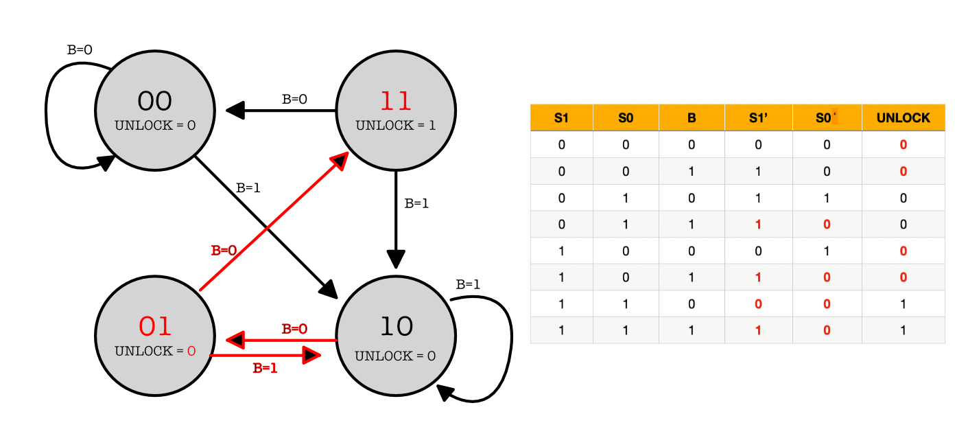
The combination for the lock is 100.
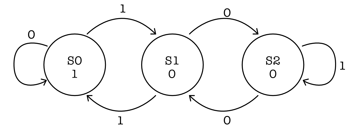
Constructing an FSM (Basic)
Construct a “divisible-by-3” FSM that accepts a binary number entered one bit at a time, most significant bit first, and indicates with a light if the number entered so far is divisible by 3. Answer the following questions:
- Draw a state transition diagram for your FSM indicating the initial state and for which states the light should be turned on. Hint: the FSM has 3 states.
Show Answer
If the value of the number entered so far is N, then if digit b is entered next, the value of the new number N' is 2N + b. Using this fact:
- If N is 0 mod 3 then for some p, N = 3p + 0. After the digit b is entered, N' = 6p + b. So N' is b mod 3.
- If N is 1 mod 3 then for some p, N = 3p + 1. After the digit b is entered, N' = 6p + 2 + b. So N' is b+2 mod 3.
- If N is 2 mod 3 then for some p, N = 3p + 2. After the digit b is entered, N' = 6p + 4 + b. So N' is b+1 mod 3.
This leads to the following transition diagram where each state corresponds to each of the possible values of N mod 3.
- Construct a truth table for the FSM logic. Inputs include the state bits and the next bit of the number; outputs include the next state bits and the control for the light.
Show Answer
$$ \begin{matrix} S_1 & S_0 & b & S_1' & S_0' & \text{light} \\ \hline 0 & 0 & 0 & 0 & 0 & 1 \\ 0 & 0 & 1 & 0 & 1 & 1 \\ 0 & 1 & 0 & 1 & 0 & 0 \\ 0 & 1 & 1 & 0 & 0 & 0 \\ 1 & 0 & 0 & 0 & 1 & 0 \\ 1 & 0 & 1 & 1 & 0 & 0 \\ \hline \end{matrix} $$
- Write down the boolean equation for the FSM.
Show Answer
$$ \begin{aligned} \text{light } &= \overline{S_1} * \overline{S_0}\\ S_1' &= \overline{S_1} * S_0 * \overline{b} + S_1 * \overline{S_0} * b \\\\ S_0' &= \overline{S_1} * \overline{S_0} * b + S_1 * \overline{S_0} * \overline{b} \end{aligned} $$
Hardware Implementation of a state machine (Intermediate)
Consider the schematic of a machine as follows, which function is to: detect a sequence of three or more consecutive 1’s, and output: 1 after three or more consecutive 1’s, or 0 otherwise.
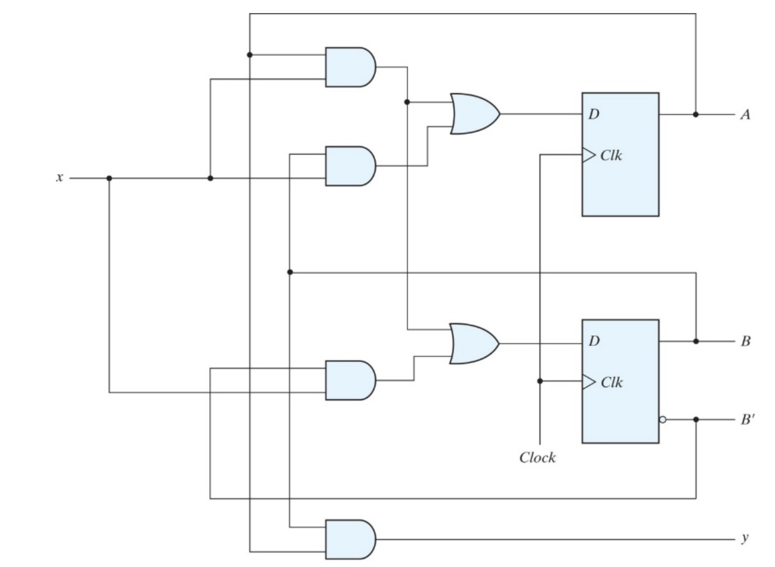
Let’s analyse the circuit by answering the questions below:
- If the circuit has an initial state of
AB=00, and the input att=0isx=0, what will the immediate next state be?Show AnswerThe immediate next state is:
AB = 00. You can easily trace this output from the circuit above. - If the circuit has an initial state of
AB=00, and the input att=0isx=1, what will the immediate next state be?Show AnswerThe immediate next state is:
AB = 01. You can easily trace this output from the circuit above. - If the circuit has a current state
AB=01, and the current input isx=1, what will the immediate next state be?Show AnswerThe immediate next state is:
AB = 10. You can easily trace this output from the circuit above. - If the circuit has a current state
AB=11, and the current input isx=1, what will the immediate next state be?Show AnswerThe immediate next state is:
AB = 11. You can easily trace this output from the circuit above. - If the circuit has a current state
AB=11, and the current input isx=0, what will the immediate next state be?Show AnswerThe immediate next state is:
AB = 00. You can easily trace this output from the circuit above. -
What are the state(s) that can go to state
AB=00as its next state?Show AnswerAll combinations:
AB=00, 01, 10, or11. You can prove it easily by brute force: checking ifAB = 00next if its previously set to some valueAB = ijgiven existing valuex. - What is the value of output
ywhen the current state isAB = 11and the current input isx = 0?Show AnswerTracing it out, we have
y=1. - The propagation delays for all the combinational logic gates and the flip-flops are
2ns. The clock frequency is100MHz. What is the worst case delay in nanosecond for the next states atAandBto appear (i.e. forAandBto be valid) after the inputxis changed to be a valid input. Assume that the initial statesABare given and fixed.Show AnswerFrom the frequency, we can compute the period of the clock to be
10ns.
For the worst case delay, we need to consider the scenario that inputxis propagated up to input of the register and it just missed theclkrise. It takes4nsto propagate through theANDandORgates, and another10nsto wait for anotherclkrise. Finally, it takes2nsto propagate through the register to produceAorB. Hence the worst case delay is4+10+2 = 16ns. -
The propagation delays for all the combinational logic gates and the flip-flops are
2ns. Eachdffhave $t_H$ and $t_S$ of1nseach. If the clock frequency is not given, what is the maximum clock frequency (smallestclkperiod) that we can have for this device?Show AnswerThe clock period has to satisfy the feedback path ($t_2$ timing constraint), that is made up with $t_{PD}$ of the
dff, $t_{PD}$ of theANDgate, $t_{PD}$ of theORgate, plus $t_S$ of the register. This adds up to2+2+2+1 = 7ns. Hence the maximum frequency is $\frac{1}{(7*10^{-9})}$= 142.9MHz</code. </p> </div>
- What are the output sequences from
t=1tot=16of the circuit when fed the following input (fed from left to right):1101 1111 1110 0010fromt=0tot=15respectively? Assume that the initial states areAB=00.Show AnswerGiven that the initial state is
AB=00, that makesB = 1att=0. This is doable the tedious way by simply tracing the outputysixteen times fromt=1tot=16. We can also deduce from the functionality of the device, that is to detect three consecutive1's and output0afterwards. The output sequence is therefore0000 0011 1111 0000fromt=1tot=16. repectively.
State-Machine Timing Computation (Intermediate)
Take a look at the following State Machine circuitry:
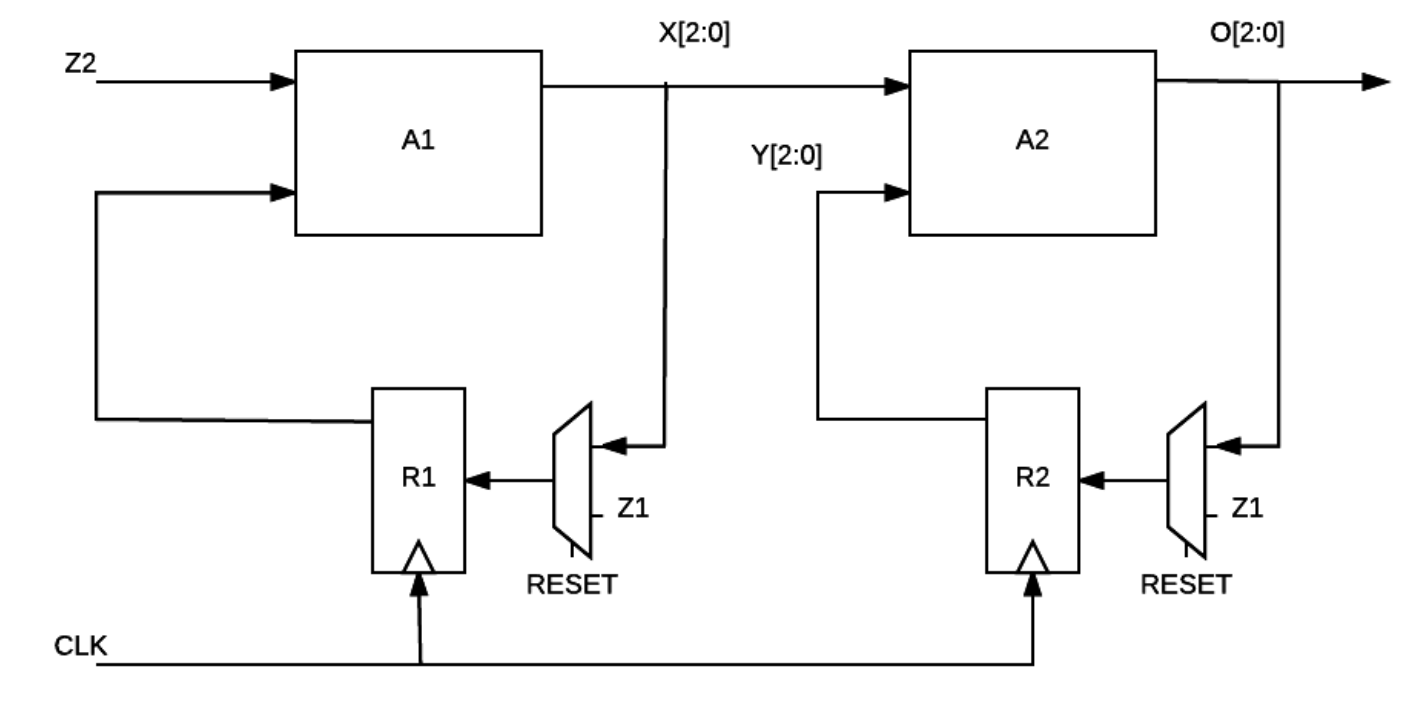
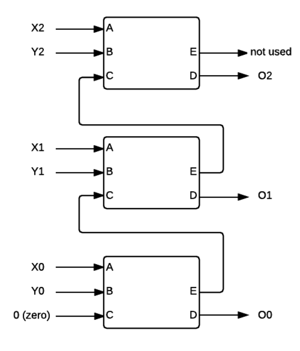
The device A2 has the following schematic:
It is made out of this device we call A000R with $t_{CD}$ = 1ns, and $t_{PD}$ = 3ns with the following schematic:
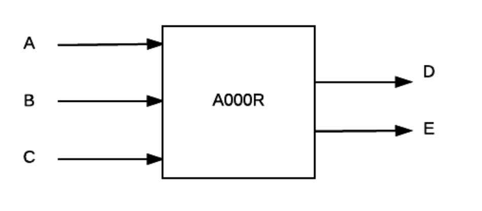
The truth table for A000R is as follows:
The timing specifications for other devices in the state machine is:
-
The Mux has the following time specification: $t_{CD}$ =
1ns, and $t_{PD}$ =2ns. -
The Registers has the following time specification: $t_{CD}$ =
2ns, $t_{PD}$ =5ns, $t_S$ =2ns, $t_H$ =2ns.
Both A1 and A2 are combinational logic that contains A000R only. Unfortunately, the design for A1 is missing. We only know that A1 uses only A000R to compute the output and the next state function and that A1 has the same $t_{PD}$ as A2. The other information that we have is that the output of A1, X[2:0] is a sequence of decimal, [1, 2, 3, ... ] in the binary form, i.e. [001, 010, 011, ...].
Answer the following questions:
- How many bits should the constant
Z1have?Show AnswerSince one of the inputs to the muxes are 3-bits, this hardware is implemented using three 2-input mux.
Z1is essentially three bits, connected to each of the three copies of 2-input muxes. - How many bits should the constant
Z2have?Show Answer1 bit. The number of bits of each input to a combinational logic device such as
A1does not depend on anything else or other inputs. - What is the decimal value of
Z1?Show AnswerSince
X[2:0]produces an increasing sequence from decimal value of1,2,3,4,...etc, we can easily guess that the the decimal value ofZ1should be0, such that when there's aRESET, the output of the registerR1is zero. - What is the decimal value of
Z2?Show AnswerZ2's decimal value is1. The same reason applies: since the sequenceX[2:0]produced byA1is increasing by 1, the input toA1should be 1 such that at *every* cycle, theres an addition of 1 to be produced atX. - What is the $t_{PD}$ of
A2in nanosecond?Show AnswerThe $t_{PD}$ of
A000Ris 3ns, hence the $t_{PD}$ ofA2is9nssince it is made out of threeA000Rmodules connected in series. - What is the minimum clock period in nanosecond?
Show Answer
The longest path that the clock period has to satisfy is
R1 -> A1 -> A2 -> Z1 -> R2. Hence we need to consider the $t_{PD}$ of all devices in its path (exceptR2) plus $t_S$ ofR2: 5+9+9+2+2 = 27ns. - What is the minimum $t_{CD}$ of
A1in nanosecond such that $t_H$ of input (Z2) can be 0?Show Answer$t_{CD}$ of
A1has to be large enough so as to satisfy $t_H$ ofR1. $t_H$ ofR1is2ns, and $t_{CD}$ of the mux is1ns. Therefore min $t_{CD}$ ofA1is2-1 = 1ns. - What is value of
A2’s $t_{CD}$ in nanosecond?Show AnswerThe $t_{CD}$ of
A2is basically the $t_{CD}$ of a singleA000R (1ns)since that is the shortest path from any input to any output inA2. - When
RESETis1for several cycles, what will be the value ofX[2:0]?Show AnswerWhen
RESETis1, the output ofR1will be000. Hence the value ofX[2:0]will be001.. - When X’s output is sequences of value
[1, 2, 3, ...], what is the value ofRESET?Show AnswerRESEThas to be0to enable the addition of the previous value of X to take effect, and form a new value of X in the next clock cycle.
Now, suppose that at time t=0, RESET signal is changed from 1 to 0, and X becomes 001. From then on, RESET remains 0:
- What is the decimal value of
O[2:0]at timet = 0?Show AnswerXis001andYis000att=0. Using the truth table ofA000Rand the schematic ofA1, we can deduce thatO[2:0]att=0is1. - What is the decimal value of
O[2:0]at timet = 1?Show AnswerXis010andYis001att=1. Using the truth table ofA000Rand the schematic ofA1, we can deduce thatO[2:0]att=1is3. - What is the decimal value of
O[2:0]at timet=3?Show AnswerXis011andYis011att=2. Using the truth table ofA000Rand the schematic ofA1, we can deduce thatO[2:0]att=3is2.
FSM Possibility (Basic)
We saw that certain functions, such as parentheses checking, cannot be performed by any finite state machine. Which of the following can be performed by an FSM?
Assume, in each case, that the device is to take a series of 0s and 1s that represent the digits of a binary number entered left-to-right.
- The device is to have a single output, which is 1 only under this specific condition: when the last 277 digits entered have been alternate
1s and0s.Show AnswerYes. It is a bit tedious for 277 digits, but you should be able to sketch FSM for 3 or 4 digits.
-
The device is to have a single output, which is 1 only under this specific condition: when more 0s than 1s have been entered.
Show AnswerNo. Requires unbounded counting.
-
The device is to have a single output, which is 1 only under this specific condition: when the number entered thus far is divisible by 3.
Show AnswerYes, can be done by a 3-state machine.
-
The device is to have a single output, which is 1 only under this specific condition: when an odd number of 1s and and even number of 0s have been entered.
Show AnswerYes,, can be done with a 4-state machine.