 Computation Structures
- Problem Set 2
- CMOS Technology
- Logic Synthesis
- CMOS Circuit Boolean Expression (Basic)
- Combinational Circuit’s Functional Specs (Basic)
- Simple Boolean Algebra (Basic)
- Reading ROM (Basic)
- Implementing Half-Adder using ROM (Basic)
- CMOS Gate Analysis (Basic)
- Simplifying a Rather Complicated Boolean Expression (Intermediate)
- CMOS Gate Design (Challenging)
- Another Boolean Minimisation (Basic)
50.002 Computation Structures
Information Systems Technology and Design
Singapore University of Technology and Design
Problem Set 2
This page contains all practice questions that constitutes the topics learned in Week 2: CMOS Technology and Logic Synthesis.
Each topic’s questions are grouped into three categories: basic, intermediate, and challenging. You are recommended to do all basic problem set before advancing further.
CMOS Technology
You can refer to the notes here if you need to revise.
Combinational Logic Timing (Basic)
Consider the following combinational logic device.
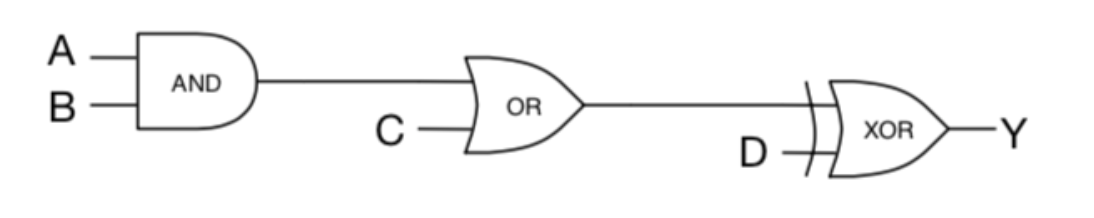
Each logic gate has the same:
- Propagation delay, $t_{pd}$= 2ns,
- Contamination delay, $t_{cd}$=1ns
Compute the overall propagation delay and contamination delay for the circuit.
Overal $t_{pd}$ = 6ns, $t_{pd}$ = 6ns (counting paths from the AND gate, OR gate, and XOR gate).
Overall $t_{cd}$ = 1ns, $t_{cd}$ = 1ns (counting the shortest path from XOR gate).
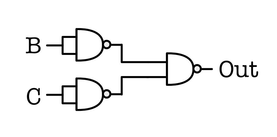
Tracing CMOS Circuit (Basic)
Draw the truth table for the following CMOS circuitry:
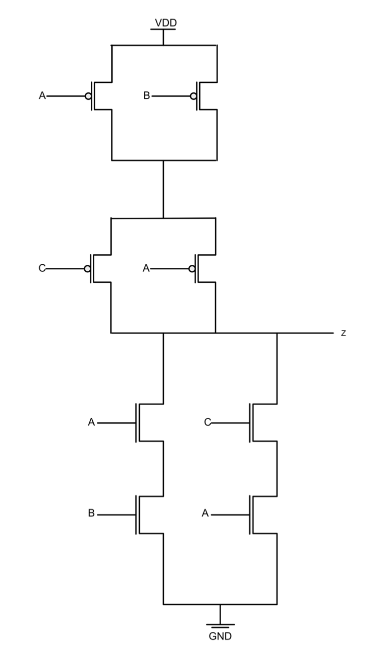
$$ \begin{matrix} A & B & C & OUT \\ \hline 0 & 0 & 0 & 1 \\ 0 & 0 & 1 & 1 \\ 0 & 1 & 0 & 1 \\ 0 & 1 & 1 & 1 \\ 1 & 0 & 0 & 1 \\ 1 & 0 & 1 & 0 \\ 1 & 1 & 0 & 0 \\ 1 & 1 & 1 & 0 \\ \hline \end{matrix} $$
Universal Gates (Basic)
Use only NAND gates to redraw the circuit below. Use as few NAND gates as possible.
If you directly convert with just NAND gates then you'll get:
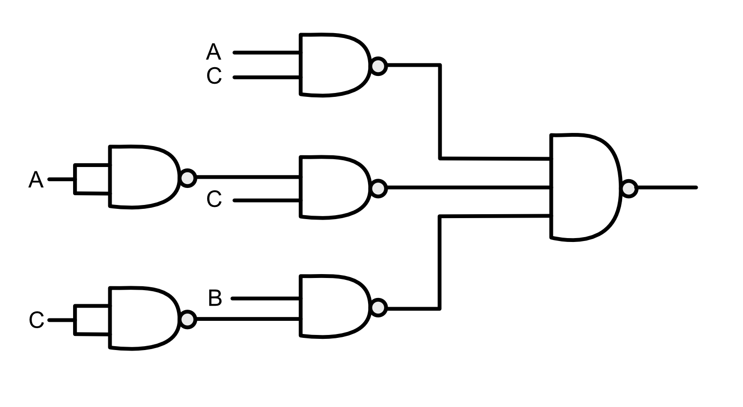
You can minimise them first by minimising the boolean expression: $$AC + \bar{A}C + B\bar{C} = C+B\bar{C} = C + B = \overline{\bar{C}\bar{B}}$$ Then we can easily draw this:
Full Adder Timing Analysis (Intermediate)
Refer to the FA circuitry below:
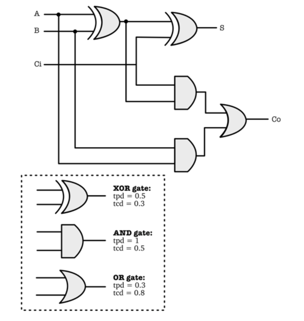
Answer the following questions:
- Compute the $t_{pd}$ and $t_{cd}$ of the full adder above.
-
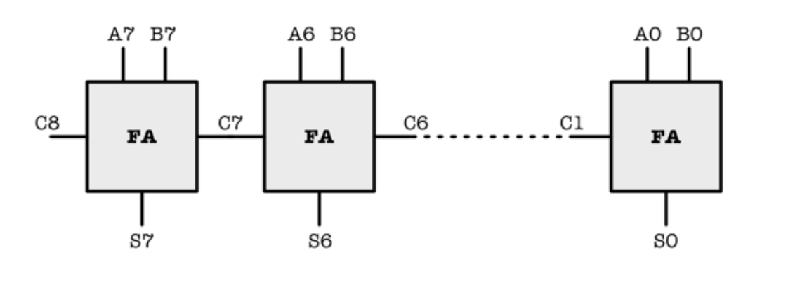
If we were to put several of these FAs to form an 8-bit ripple-carry adder as shown, compute the $t_{pd}$ and $t_{cd}$ of an 8-bit ripple-carry adder made of 8 of these FA circuits.
Hint: In the figure, $C_0$ is assumed to be grounded for this particular instance, so this sample device can only add two numbers and not subtract them.
However, is the computation of $t_{pd}$ and $t_{cd}$ of an 8-bit ripple carry adder usage specific?
- The $t_{pd}$ is 1.8 and the $t_{cd}$ is 0.3 for a single FA.
- For the 8-bit ripple-carry adder, we do not have an input $C_0$ as it is grounded However the $t_{cd}$ is still 0.3 as the specification of contamination delay is not usage specific. Its $t_{pd}$ is approximately 8 times bigger than a single FA $\rightarrow$ $t_{pd}$= 14.4. To be exact, if $A_i$ XOR $B_i$ is parallel, meaning that $A_i$, $B_i$ are given and valid at the same time for all adder units $i=0,1,...7$, then the $t_{pd}$ is $1.8+7\times1.3=10.9$.
However if the question is asking for the $t_{cd}$ of this particular device with no $C_0$ input terminal at all then the answer is $0.6$ns since there's no $C_0$.
Combinational Construction Rules (Challenging)
During lecture, we learned a first set of principles that define a combinational device. A combinational device is a circuit element that has:
- One or more digital inputs
- One or more digital outputs
- A functional specification that details the value of each output for every possible combination of valid input values
- A timing specification consisting (at minimum) of an upper bound $t_{pd}$ on the required time for the device to compute the specified output values from an arbitrary set of stable, valid input values.
We also learned a second set of rules, that a set of interconnected elements is a combinational device if:
- Each circuit element is combinational
- Every input is connected to exactly one output or to some vast supply of 0’s and 1’s.
Note: read this carefully. This does NOT mean that a combinational device must just have one output and one input. This means that *for each input of a combinational device*, it is connected to *exactly ONE output* of the “previous” device.
- The circuit contains no directed cycles
In this problem, we ask you to think carefully about why these rules work - in particular, why an acyclic circuit of combinational devices, constructed according to the second principle, is itself a combinational device as defined by the first.
Consider the following 2-input acyclic circuit whose two components, A and B, are each combinational devices.
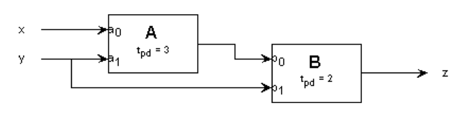
The propagation delay for each device is specified in nanoseconds.
The functional specifications for each component are given as truth tables detailing output values for each combination of inputs, where $A _{a_0, a_1}$ denotes the output from device A, and $B _{b_0, b_1}$ denotes the output from device B:
\[\begin{matrix} a_0 & a_1 & A _{a_0, a_1} & b_0 & b_1 & B_{b_0, b_1}\\ \hline \\ 0 & 0 & 1 & 0 & 0 & 0\\ 0 & 1 & 0 & 0 & 1 & 0\\ 1 & 0 & 0 & 1 & 0 & 0\\ 1 & 1 & 1 & 1 & 1 & 1\\ \hline \end{matrix}\]Answer the following questions,
-
Give a truth table for the overall acyclic circuit, i.e. a table that specifies the value of z for each of the possible combinations of input values on x and y.
-
Describe a general procedure by which a truth table can be computed for each output of an arbitrary acyclic circuit containing only combinational components. Hint : construct a functional specification to each circuit node.
-
Specify a propagation delay (the upper bound required for each combinational device) for the circuit.
-
Describe a general procedure by which a propagation delay can be computed for an arbitrary acyclic circuit containing only combinational components. \textit{Hint: add a timing specification to each circuit node}.
-
Do your general procedures for computing functional specifications and propagation delays work if the restriction to acyclic circuits is relaxed (lifted)? Explain.
- The truth table is as follows: $$\begin{matrix} x & y & z \\ \hline 0 & 0 & 0 \\ 0 & 1 & 0 \\ 1 & 0 & 0 \\ 1 & 1 & 1 \\ \hline \end{matrix}$$
- We can construct the truth table from left to right, i.e: solve the truth table for each component from the leftmost all the way to the rightmost, one by one.
- The total propagation delay is the sum of each device's (A and B) propagation delay: $3 + 2 = 5$.
- One has to find the longest path from (any) input to (any) output to find the total propagation delay of the combinational circuit.
- No, the signal can propagate back into the circuit's input so using the longest path to calculate $t_{pd}$ is not applicable anymore.
Logic Synthesis
You can refer to the notes here if you need to revise.
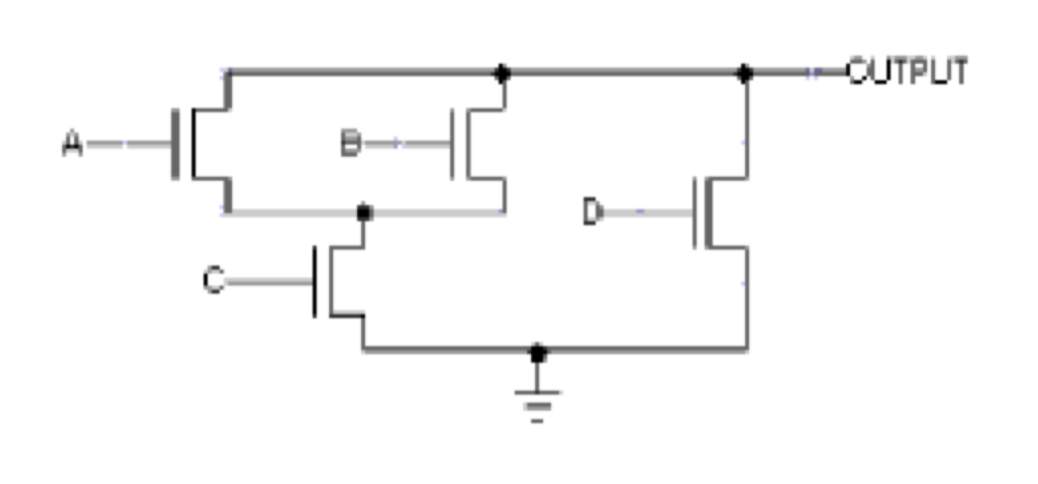
CMOS Circuit Boolean Expression (Basic)
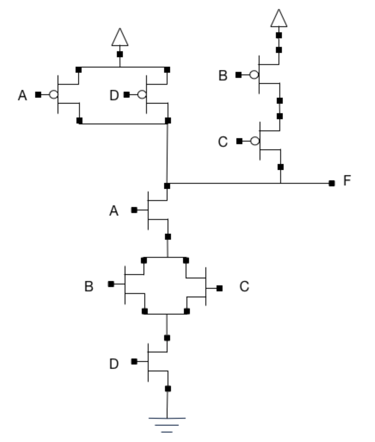
- Draw the truth table of the CMOS circuit above.
- What is the boolean expression for the CMOS circuit shown?
1. The truth table of the CMOS circuit contains 16 lines since theres $2^4$ possible input combinations and 1 possible output bit:
$$\begin{matrix}
A & B & C & D & F \\ \hline 0 & 0 & 0 & 0 & 1 \\ 0 & 0 & 0 & 1 & 1 \\ 0 & 0 & 1 & 0 & 1 \\ 0 & 0 & 1 & 1 & 1 \\ 0 & 1 & 0 & 0 & 1 \\ 0 & 1 & 0 & 1 & 1 \\ 0 & 1 & 1 & 0 & 1 \\ 0 & 1 & 1 & 1 & 1 \\ 1 & 0 & 0 & 0 & 1 \\ 1 & 0 & 0 & 1 & 1 \\ 1 & 0 & 1 & 0 & 1 \\ 1 & 0 & 1 & 1 & 0 \\ 1 & 1 & 0 & 0 & 1 \\ 1 & 1 & 0 & 1 & 0 \\ 1 & 1 & 1 & 0 & 1 \\ 1 & 1 & 1 & 1 & 0 \\ \hline \end{matrix}$$
2. $F = \overline{A(B+C)D}$
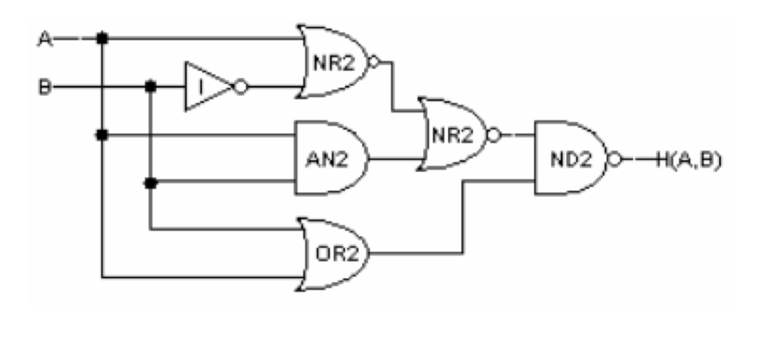
Combinational Circuit’s Functional Specs (Basic)
Consider the following circuit that implements the 2-input function $H(A,B)$:
-
Write down the truth table for $H$.
- Give a sum-of-products expression that corresponds to your truth table.
- Using the information below, what are the $t_{cd}$ and $t_{pd}$ of the circuit?
- $t_{cd}$ and $t_{pd}$ of NR2: 5, 30
- $t_{cd}$ and $t_{pd}$ of ND2: 5, 30
- $t_{cd}$ and $t_{pd}$ of AN2: 6, 50
- $t_{cd}$ and $t_{pd}$ of OR2: 10, 20
- $t_{cd}$ and $t_{pd}$ of INV: 1, 3
- The truth table is as follows: $$\begin{matrix} A & B & H \\ \hline 0 & 0 & 1\\ 0 & 1 & 1 \\ 1 & 0 & 0 \\ 1 & 1 & 1\\ \hline \end{matrix} $$
- We begin by finding the expression of the topmost two circuits and applying de Morgan's law $$\overline{A + \overline{B}} = \overline{A}B$$
Then, we find the expression of the next pair, which is $AB$. We combine this with the above using a NOR gate and reduce the result, $$\overline{\overline{A}B + AB} = \overline{B}$$
Finally, we find the expression for the bottom two pairs, which is simply $A+B$. Combining this with the above expression, we reduce and apply de Morgan's law: $$\begin{aligned} \overline{(A+B)\overline{B}} &= \overline{A \overline{B} + B \overline{B}} = \overline{A\overline{B}} = \overline{A} + B\\ \end{aligned}$$ - The contamination delay is the path (from any input to any output) that results in the shortest time: NR2 + NR2 + ND2 = $5 + 5 + 5 = 15$. The propagation delay is the path (from any input to any output) that results in the longest time: AN2 + NR2 + ND2 = $50 + 30 + 30 = 110$.
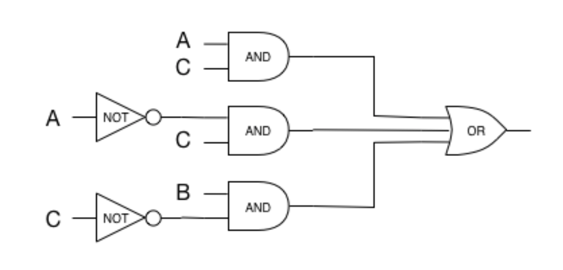
Simple Boolean Algebra (Basic)
Given the following truth table,
\[\begin{matrix} A & B & C & OUT \\ \hline 0 & 0 & 0 & 1 \\ 0 & 0 & 1 & 1 \\ 0 & 1 & 0 & 1 \\ 0 & 1 & 1 & 0 \\ 1 & 0 & 0 & 1 \\ 1 & 0 & 1 & 1 \\ 1 & 1 & 0 & 1 \\ 1 & 1 & 1 & 0 \\ \hline \end{matrix}\]Choose all the correct Boolean expression of this circuit:
-
$OUT = \bar{C} + \bar{B}$
-
$OUT = \bar{A} \cdot \bar{B} + A \cdot \bar{B} + B \cdot \bar{C}$
-
$OUT = \bar{A} \cdot \bar{C} + A \cdot B \cdot \bar{C} + \bar{B}$
-
$OUT = \bar{A} \cdot B + A \cdot B \cdot \bar{C} + \bar{B}$
(a), (b), and (c) are all equivalent and represents the truth table.
Hint: express the table in terms of sum of products first and then simplify the expression.
Reading ROM (Basic)
What is the the sum-of-products for the following ROM (Read Only Memory)?
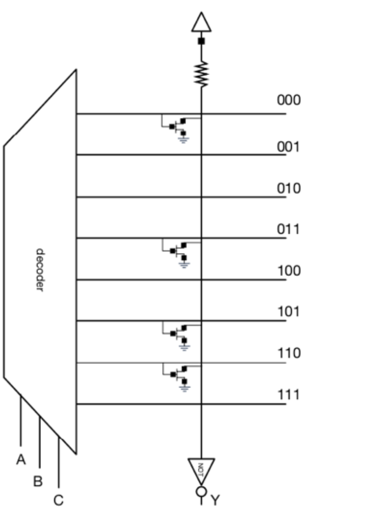
$Y = \bar{A}\bar{B}\bar{C} + \bar{A}BC + A \bar{B} C+ AB\bar{C}$.
This expression can be computed easily after you create a truth table first out of the ROM.
Implementing Half-Adder using ROM (Basic)
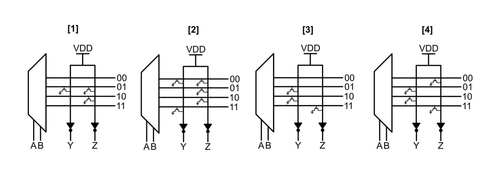
Take a look at the figure above. Which of the above ROM represents the functionality of a half adder?
ROM [3] represents half-adder functionality.
Y's output shows a XOR(A,B) while Z's output shows an AND(A,B).
Hence this make Y to be the SUM output and Z to be the CARRY output.
CMOS Gate Analysis (Basic)
The following diagram shows a schematic for the pulldown circuitry for a particular CMOS gate:
-
What is the correct schematic for the pullup circuitry?
- Assuming the pullup circuitry is designed correctly, what is the logic function (boolean function) implemented at this gate?
- Assuming the pullup circuitry is designed correctly, when the output of the CMOS gate above is a logic “0” in the steady state, what would we expect the voltage value of the output terminal to approximately be? What would be the approximate voltage output value if the output were a logic “1”?
- The output for the pullup circuitry is the inversion of the output of the pulldown circuitry:
$$\overline{(A+B) C + D} = (\overline{A} \text{ }\overline{B} + \overline{C}) \overline{D}$$
Note: We don't need to add inverter in the inputs. Convince yourself that this is true by tracing some input combinations to the output terminal.
- From the pulldown diagram, it seems like the output is 0 if D is 1, or A and C is 1, or B and C is 1. Therefore, the output for the gate is the inverse of the expression of the pulldown circuitry, which is the output of the pullup circuitry above: $\overline{(A+B) C + D} = (\overline{A} \text{ }\overline{B} + \overline{C}) \overline{D}$.
- The voltage of the output terminal at "0" steady state is 0 (GND). The voltage of the output terminal at "1" steady state is VDD's voltage.
Simplifying a Rather Complicated Boolean Expression (Intermediate)
Simplify the following boolean expression:
\[\begin{aligned} Y &= AB \bar{C} \bar{D} + AB \bar{C}D + \bar{A} \bar{B}CD + \bar{A}BCD \\ &+ ABCD + A\bar{B}CD + \bar{A}\bar{B}C \bar{D} + ABC \bar{D} + A\bar{B}C \bar{D}\end{aligned}\]
The final simplified form is $Y = AB + CD + \bar{B}C$. The steps are as follows:
$$\begin{aligned}
Y &= AB \bar{C} \bar{D} + AB \bar{C}D + \bar{A} \bar{B}CD + \bar{A}BCD + ABCD \\
& + A\bar{B}CD + \bar{A}\bar{B}C \bar{D} + ABC \bar{D} + A\bar{B}C \bar{D}\\
&= AB\bar{C} + \bar{A}CD + ACD + \bar{B}C\bar{D} + ABC\bar{D}\\
&= CD + AB\bar{C} + \bar{B}C\bar{D} + ABC\bar{D}\\
&= C(D + \bar{B} \bar{D}) + AB(\bar{C} + C\bar{D} )\\
&= C(D + \bar{B} ) + AB(\bar{C} + \bar{D} )\\
&=CD + C\bar{B} + AB(\overline{CD} )\\
&= CD + C\bar{B} + AB
\end{aligned}$$
Note: convince yourself that the simplified form allows you to make a cheaper and smaller combinational logic device (because we use lesser number of gates).
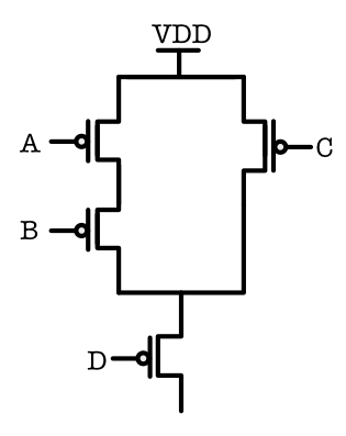
CMOS Gate Design (Challenging)
Anna Logue, a circuit designer who missed several early 6.004 lectures, is struggling to design her first CMOS logic gate. She has implemented the following circuit:
Anna has fabricated 100 test chips containing this circuit, and has a simple testing circuit which allows her to try out her proposed gate statically for various combinations of the A and B inputs.
She has burned out 97 of her chips, and needs your help before destroying the remaining three. She is certain she is applying only valid input voltages, and expects to find a valid output at terminal C. Anna also keeps noticing a very faint smell of smoke.
-
What is burning out Anna’s test chips? Give a specific scenario, including input values together with a description of the failure scenario. For what input combinations will this failure occur?
- Are there input combinations for which Anna can expect a valid output at C? Explain.
- One of Anna’s test chips has failed by burning out the pullup connected to A as well as the pulldown connected to B. Each of the burned out FETs appears as an open circuit, but the rest of the circuit remains functional. Can the resulting circuit be used as a combinational device whose two inputs are A and B? Explain its behavior for each combination of valid inputs.
- In order to salvage her remaining two chips, Anna connects the A and B inputs of each and tries to use it as a single-input gate. Can the result be used as a single-input combinational device? Explain.
- When $A=0, B=1$ or $A=1, B=0$, then there's an open connection between VDD and GND. This caused the gate to short circuit, and hence its burning out.
- Yes, when $A=1, B=1$ then $C=0$, or $A=0, B=0$, then $C=1$. This is when the pullup and pulldown circuit aren't both ON at the same time.
- No When $A=1, B=0$, the circuit will burn out again, since the pullup and pulldown will be active, thus burning out the circuit. Also, the output is not defined when $A=0, B=1$, since neither the pullup or pulldown are active.
- Yes. It exhibits the behavior of an inverter, i.e: A and B are connected to the same $V_{IN}$.
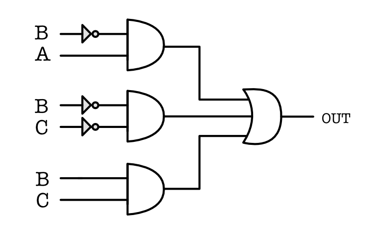
Another Boolean Minimisation (Basic)
A certain function F has the following truth table:
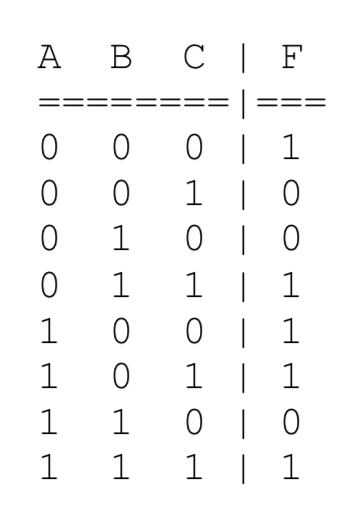
Answer the following questions based on the truth table:
-
Write a sum-of-products expression for F.
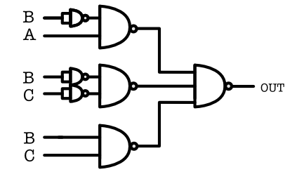
- Write a minimal sum-of-products expression for F. Show a combinational circuit that implements F using INV and OR, and AND gates. Then implement it using only NAND gates.
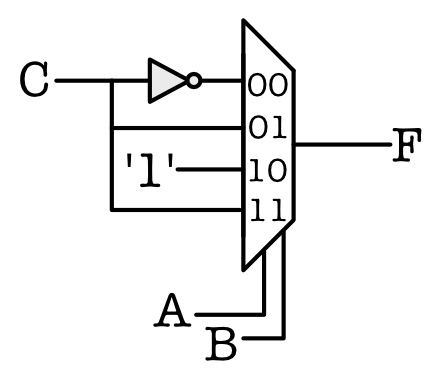
- Implement F using one 4-input MUX and inverter.
- Write a minimal sum-of-products expression for NOT(F).
- $\overline{A}\text{ }\overline{B}\text{ }\overline{C} + \overline{A}BC + A \overline{B}\text{ }\overline{C} + A \overline{B}C + ABC$
- The minimal sum of products is: $\overline{B}A + \overline{B} \text{ } \overline{C} + BC$. You can draw a combinational circuit of this by adding an input to a big OR gate for every '+', INV (where necessary for negated input) with AND gate for every *pair* of input in the minimal sum of products:
To turn AND and ORs into just NANDs, we can do this in two steps. First, turn the AND into NAND and add an inverter:
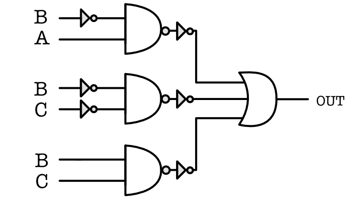
Then apply DeMorgan law:
- If we use A and B as the select inputs for the MUX, then the four data inputs of the MUX should be tied to one of "0" (ground), "1" (VDD), "C" or "NOT C". The following is one of the correct schematics that implement this function (there are other acceptable answers as well). Note that by changing the connections on the data inputs to the mux, we could implement any function of A, B and C.
- We can just write *sum of produc*t for rows that results the '0's in the table above, and then reduce the expression into: $\overline{F} = B \overline{C} + \overline{A} \text{ } \overline{B} C$ </p></div>
- on the lower right corner (row 3 and 4, with column 3 and 4),
- on the sides (row 1 and 2, with column 1 and 4), and
- on the four corners (row 1 col 1, and row 1 col 4, and row 4 col 1, and row 4 col 4).
- Let X = F(F1, F2, F3, F4), Z = G(G1, G2, G3, G4), Y = H(C1, C2, C3). The necessary control signals are:
- MA = 1
- MB = 1
- MC = 0 (select C1)
- MD = 1 (select C2)
- ME = 2 (select C3)
- Let Y = F(A1, A2, A3, A4, A5). This can be implemented using both 4-input logic functions, and selecting between the two outputs with the 3-input logic function.
- Z=f(A1, A2, A3, A4, 0),
- X=f(A1, A2, A3, A4, 1),
- Y= Z if A5=0, else Y=X
The necessary control signals are:- MA = 0
- MB = 0
- MC = X (value doesn't matter)
- MD = X (value doesn't matter)
- ME = 0 (select C1)
- Let Z = G(G1, G2, G3, G4) be the function of the 4 variables. Let X = F(F1, F2, F3, F4) and let Y = H(C1, C2, X) = H(C1, C2, F(F1, F2, F3, F4)). The functions of six variables which can be implemented (along with the 4-variable function) are all those functions that can be re-written as a function of 3 variables. The inputs to this function of three variables must be 2 of the original variables and some function of the remaining four variables. The necessary control signals are:
- MA = 0
- MB = 1
- MC = X (value doesn't matter)
- MD = 0 (select C1)
- ME = 1 (select C2)
- Let: X = F(F1, F2, F3, F4), Z = G(G1, G2, G3, G4), Y = H(C1, X, Z) = H(C1, F(F1, F2, F3, F4), G(G1, G2, G3, G4)). The functions of nine variables that can be implemented are all those functions that can be re-written as a function of 3 variables. The inputs to this three-variable function will be one of the original variables, plus two separate functions of 4 variables (these two 4-variable functions will have the remaining 8 original variables as inputs).
- MA = 0
- MB = 0
- MC = X (value doesn't matter)
- MD = X (value doesn't matter)
- ME = 0 (select C1)
- The functions of 6 variables which we can implement must be of the form: Y = C(C1, C2, F(F1,F2,F3,F4)) or the form of Y = C(C1,F(F1, F2, F3, F4), G(G1, G2, G3, G4)). This second function will have some overlap between C1, F1-4, and G1-4; some variables will be connected to multiple inputs.
Essentially, the functions we are able to implement are only those for which we can factor a set of 4 variables out of the equation. For example, the following function cannot be implemented by the CLB: Y = A1A2A3A4A5 + A1A2A3A4A6 + A1A2A3A5A6 + A1A2A4A5A6 + A1A3A4A5A6 +A2A3A4A5A6. This function cannot be broken down into either of the forms mentioned above.
## Reading Karnaugh's Map Given the following Karnaugh's Map, write its **simplified boolean equation**. $$\begin{matrix} & \bar{A} \bar{B} &\bar{A} B & AB & A\bar{B} \\ \hline \bar{C}\bar{D} & 1 & 0 & 0 & 1 \\ C\bar{D} & 1 & 0 & 0 & 1\\ CD & 0 & 0& 1 & 1\\ \bar{C}D & 1 & 0 & 1 & 1\\ \end{matrix}$$
The minimised boolean expression is $AD + \bar{B}\bar{C} + \bar{B} \bar{D}$. They're obtained from "three" boxes:
## The FPGA (Challenging) The Xilinx 4000 series field-programmable gate array (FPGA) can be programmed to emulate a circuit made up of many thousands of gates; for example, the *XC4025E* can emulate circuits with up to **25,000 gates**. The heart of the FPGA architecture is a *configurable logic block (CLB)* which has a c**ombinational logic subsection** with the following circuit diagram:
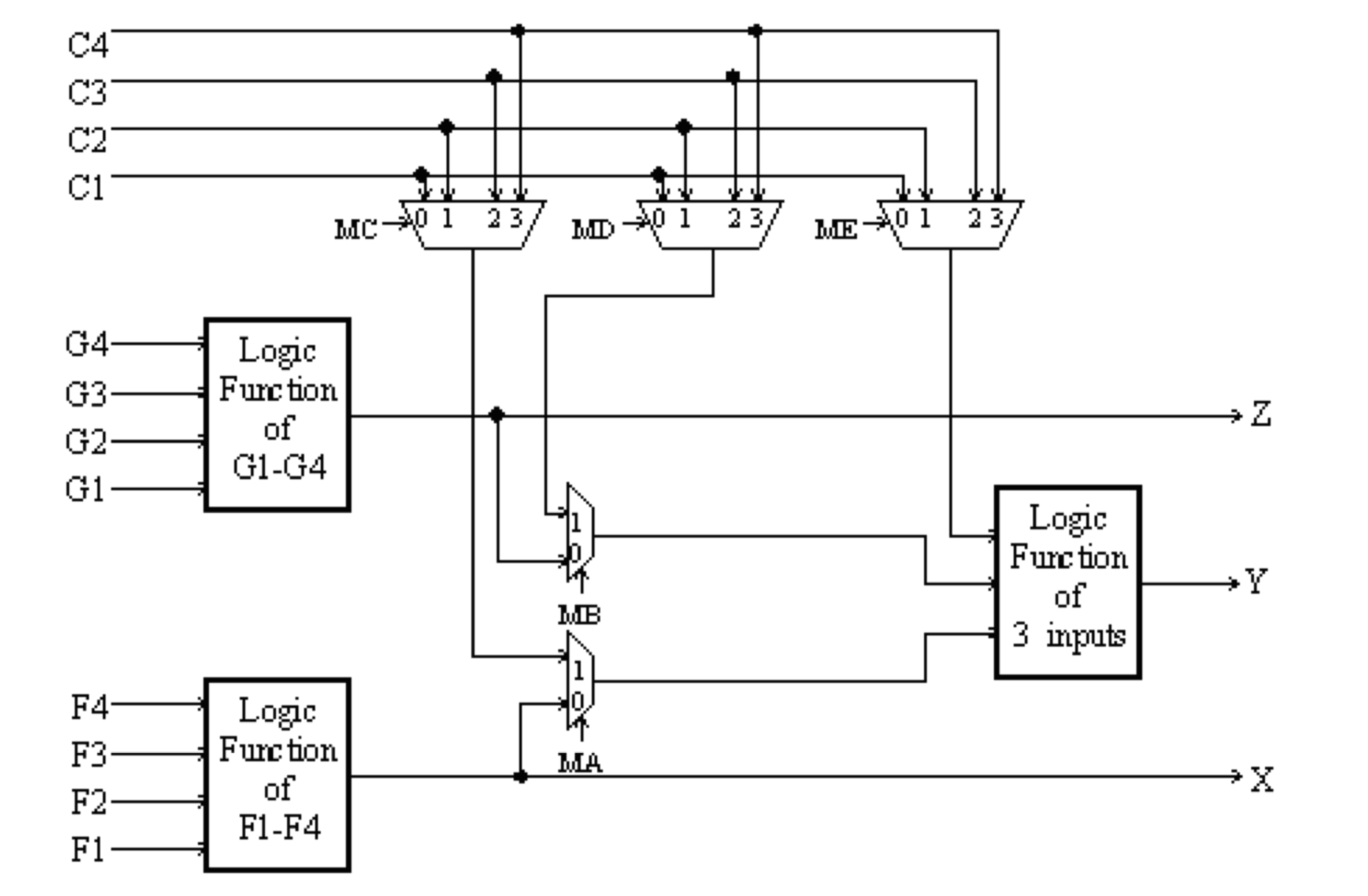 There are **two 4-input function generators** and **one 3-input function generator**, each capable of implementing an **arbitrary** Boolean function of its inputs.
The function generators are actually **small** 16-by-1 and 8-by-1 memories that are used as lookup tables. When the Xilinx device is "*programmed*" these memories are *filled with the appropriate values* so that each generator produces the desired outputs.
The multiplexer select signals (labeled "Mx" in the diagram) are also set by the programming process to configure the CLB. After programming, these Mx signals remain constant during CLB operation.
The following is **a list of the possible configurations.**
**(a)**. An arbitrary function F of **up to four unrelated input variables**, plus another arbitrary function G of **up to four unrelated input variables,** plus a third arbitrary function H of **up to three unrelated input variables.**
**(b)**. **An arbitrary single function of five variables.**
**(c)**. **An arbitrary function of four variables** together *with some functions of six variables.* Characterize the functions of six variables that can be implemented.
**(d)**. **Some functions of up to nine variables.** Characterize the functions of up to nine variables that can be implemented.
**(e)**. **Can every function of six inputs be implemented?** If so, explain how. If not, give a 6-input function and explain why it can't be implemented in the CLB.
For each configuration indicate **how**:
- Each the **control signals** (MA, MB, MC, MD, and ME) should be programmed?
- Which of the **input lines** (C1-C4, F1-F4, and G1-G4) are used?
- And what **output lines** (X, Y, or Z) the result(s) appear on?
There are **two 4-input function generators** and **one 3-input function generator**, each capable of implementing an **arbitrary** Boolean function of its inputs.
The function generators are actually **small** 16-by-1 and 8-by-1 memories that are used as lookup tables. When the Xilinx device is "*programmed*" these memories are *filled with the appropriate values* so that each generator produces the desired outputs.
The multiplexer select signals (labeled "Mx" in the diagram) are also set by the programming process to configure the CLB. After programming, these Mx signals remain constant during CLB operation.
The following is **a list of the possible configurations.**
**(a)**. An arbitrary function F of **up to four unrelated input variables**, plus another arbitrary function G of **up to four unrelated input variables,** plus a third arbitrary function H of **up to three unrelated input variables.**
**(b)**. **An arbitrary single function of five variables.**
**(c)**. **An arbitrary function of four variables** together *with some functions of six variables.* Characterize the functions of six variables that can be implemented.
**(d)**. **Some functions of up to nine variables.** Characterize the functions of up to nine variables that can be implemented.
**(e)**. **Can every function of six inputs be implemented?** If so, explain how. If not, give a 6-input function and explain why it can't be implemented in the CLB.
For each configuration indicate **how**:
- Each the **control signals** (MA, MB, MC, MD, and ME) should be programmed?
- Which of the **input lines** (C1-C4, F1-F4, and G1-G4) are used?
- And what **output lines** (X, Y, or Z) the result(s) appear on?