 Computation Structures
50.002 Computation Structures
Information Systems Technology and Design
Singapore University of Technology and Design
Sequential Logic and Synchronization
Overview
So far we have learned the basics of combinational logic device, which is in essence a device that is capable to adhere to a given functional specification (truth table). One apparent feature of a combinational logic device is that its output always depends on the current input. However, external input is unreliable, and there’s no guarantee that the input will be available for at least $t_{pd}$–until the combinational device produces meaningful results. We need to find a way to synchronize the external input signal such that there’s enough time for the entire circuit to finish its computation properly.
We also need to create another type of device, called the sequential logic device, whereby its output depends not only on the current input, but a series of past inputs as well. If a sequential logic device has a finite number of states, it also known as the finite state machine (FSM). The FSM can be seen as an abstract mathematical model of a sequential logic function. More about FSM can be learned in the next chapter.
However, our knowledge so far is not enough to create sequential logic devices. To synchronize and remember the series of past inputs, we need to have some kind of storage (memory) device.
Recap: simple combinational logic device does not remember its output value. It only gives an output when there’s an input, and the output(s) stay(s) stable for as long as its input(s) is/are stable.
A memory device on the other hand, is a device of which we can write new values to and is able to remember this value for a period of time.
We can connect memory device(s) together with combinational logic device(s) to form a sequential logic device. Notice the presence of a CLK below.
A sequential logic device has a general structure as shown below:
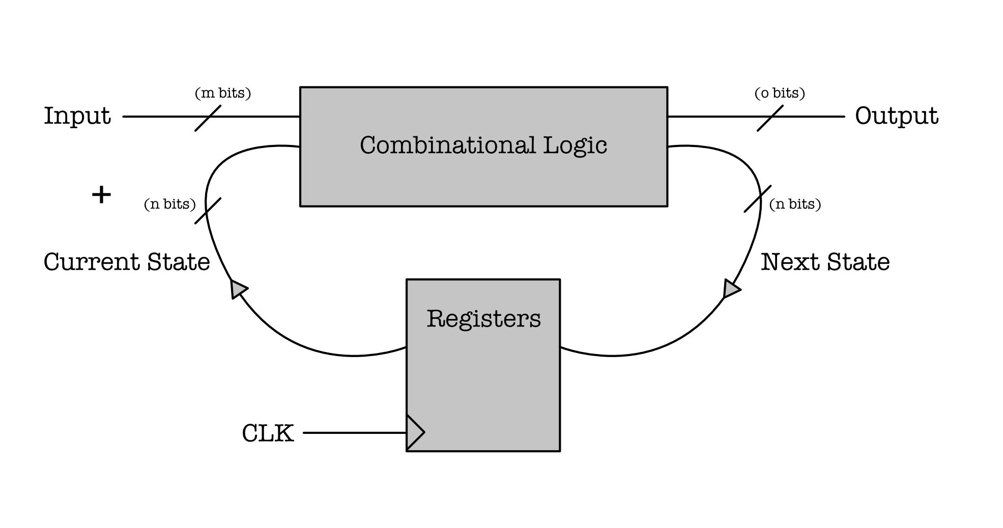
In the next few sections we will learn how to create this memory device labeled as Registers above (or more specifically, it is called D Flip-Flop).
Storage Device: D-Latch
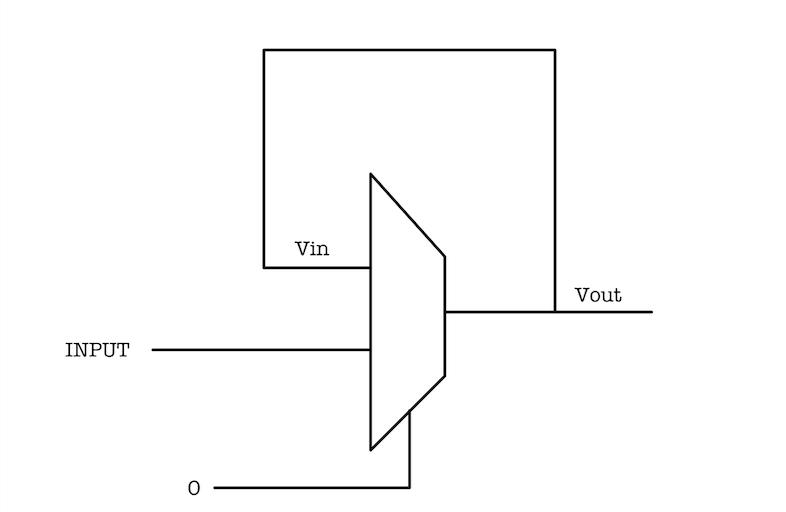
A D Flip-Flop (memory device) is made using another device called a D-latch. A D-latch can be created using a multiplexer with a feedback loop,
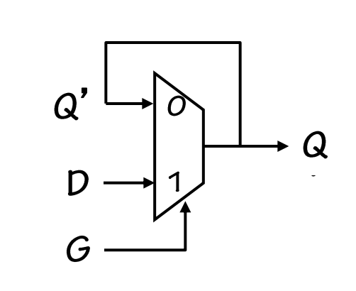
Note: this is not the only way to make a D-latch. A simple Google search will present you with some other alternatives. We just use a multiplexer here to explain the idea easily.
How it works:
-
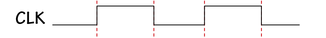
In practice, G is clock (CLK) signal. It will periodically switch between ‘1’s and ‘0’s (valid high voltage and valid low voltage) as shown in the image below:
- Q is the output of the latch, and D is the (external) input that’s placed at the second input port the latch.
-
Q is fed back as Q’, the first input port of the latch.
-
If G is 1, then the input signal on wire D will be “passed” to / reflected at output wire Q, independent of the signal on wire Q’. Lets call this the write mode. <div class="redborder">The word “pass” through is used from this point onwards in this chapter to easily explain the behavior of the mux, that when G=1, then value at Q always reflects the value at D. However recall from from Week 1 lecture (CMOS) that the signal at Q is actually due to the VDD or GND and D is simply the input at the gate that activates or deactivates the pull-up or pull-down components of the latch.</div>
- If G is 0, then output signal on wire Q reflects the signal on wire Q’, independent of input wire D. Lets call this the read memory mode.
How we intend to use the device:
We supply input voltage (valid low or high) at wire D, and simultaneously supply valid high voltage at G (or illustrated as Clock port in the figure below).
Then after some time, we supply valid low voltage at G. Hopefully at Q now we have the value that was supplied at D when G was high without having to hold D’s value(s) as they were.
If we put many of these devices in parallel, we can have a fixed N-bit output that is “remembered” by the device without having to always supply these combination of values at the input ports D. We can then use the output of these memory devices as an input to the combinational logic device for at least as long as its $t_{pd}$ (to finish computation). Hopefully, we then don’t have to worry about unreliable external input anymore.
The figure below illustrates an example of 4-bit input and corresponding 4-bit output. Each of the device drawn as a rectangle (with the “>” symbol at its lower left corner) is called a Flip-Flop (see later section). They are made up of D-latches.
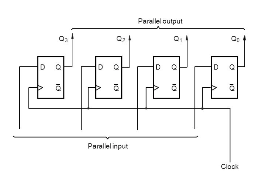
Note: From this point onwards, ‘1’ simply means valid high voltage, and ‘0’ means valid low voltage .
There are two problems that arises from using this simple D-latch in our electronic devices without any contract / rules:
-
Storage of invalid information: If G changes from
1to0at the exact moment when D just turned invalid from previously being valid, then we might end up storing that invalid value of D when the latch enters memory mode. -
Invalid/unstable output due to transition in input: If the existing stable input value in D is flipped, e.g: is changed from ‘1’ to ‘0’ or vice versa, the value at D will be invalid (momentarily) during this transition. The voltage value at D can also be invalid (unstable, unreliable) due to any disturbance.
This will affect the output at Q if G is 1, because it will pass all input from D to the output wire Q, regardless of whether it is a valid or stable input or not (during transition or any disturbance). We end up with potentially unstable/invalid output half the time.
In practice, this is not acceptable because we do not want our electronic devices (e.g: computers) to have invalid output computed (e.g: be unstable, or hang, or freeze) at any point in time, even when D is transitioning. We want it to be robust, and reliable at all times.
Combinational component within an electronic device requires a certain amount of time ($t_{pd}$) to produce meaningful results; and over this time-frame we need to hold its input stable, however external input is *unreliable* so theres no guarantee that this requirement is fulfilled.Therefore, we create another device to using D-latches, and they are called D Flip-Flop or more informally a Register to synchronize external input with the circuit’s CLK, and also switch between write and memory mode as we intend it to behave.
A D Flip-Flop with a right CLK setup will be able to produce a valid and stable output for an entire clock period – long enough for any combinational logic connected downstream to finish its computation ($t_{pd}$) and produce meaningful output before the next output value is produced.
We address these problems in the next two sections.
The Dynamic Discipline
The dynamic discipline is a contract that is made to address the first problem above: the possibility of storing invalid information in the memory device. It is imperative to never violate the dynamic discipline to ensure any sequential logic circuits to work properly.
The dynamic discipline states that there are two timing requirements for the input signal supplied at D, named as $T_{setup}$ and $T_{hold}$, which lengths are:
-
$T_{setup}$ = approximately $2 \times t_{pd}$ of the components that make up the D-latch.
-
$T_{hold}$ = approximately $t_{pd}$ of the components that make up the D-latch.
$T_{setup}$ is defined as the minimum amount of time that the voltage on wire D needs to be valid/stable BEFORE the clock edge changes from ‘1’ to ‘0’ (turning from write mode to memory mode).
$T_{hold}$ is defined as the minimum amount of time that the voltage on wire D needs to be valid/stable AFTER the clock edge reaches a valid ‘0’ from a previous ‘1’.
As explained in the previous notes, $t_{pd}$ is the propagation delay of the combinational logic devices (components) that make up a D-latch, e.g: a multiplexer, which has a $t_{pd}$ value. The multiplexer can be made using a handful NAND gates. To clarify, this $t_{pd}$ is the propagation delay of that multiplexer or components (combinational logic devices) that are used to make up a D-latch.
Why are the lengths for $T_{setup}$ and $T_{hold}$ dependent on the the $t_{pd}$ of the components that make up the D-latch?
For $T_{setup}$, you can figure this out by thinking, how long you should wait to ensure that the output signal at Q reflects what was supplied at D (requires $1\times t_{pd}$), and to ensure that this output at Q maintains this value when CLK at G turns
0(from Q’, requires another $1\times t_{pd}$).
For $T_{hold}$, you can figure this out by realising that CLK is an input to the D-latch system as well, and the device needs some time ($1\times t_{pd}$) to realise that it is in memory mode after CLK turns to a valid
0. Throughout this brief period. of time, the input at D must be held valid/stable.
Edge-Triggered D Flip-Flop
To address the second problem : the presence of unstable/invalid output during transition of input, we need to create another device called the Edge-Triggered D Flip Flop (or shortened as Flip-Flop) by putting two D-Latches in series as shown:
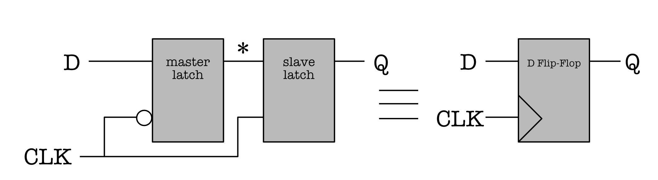
At first, each of the two rectangles are the symbol of a regular D-latch. Putting them in series (and inverting the CLK signal fed to the first latch) results in a Flip-Flop (the rectangular symbol on the right). The difference is that in a Flip-Flop, the CLK input port is represented by the > symbol at its lower left corner.
We can decribe the structure of a Flip-Flop as follows:
-
The first D-latch that receives the external input D is called the master latch, and the second D-latch is called the slave latch.
- There is an inverter applied on the G input on the master Flip-Flop, so the master latch receives or “sees” the inverted clock signal.
- The star ($\star$) symbol represents the intermediary output and its not observable outside of the system.
- The output at the Q port of the slave latch is the observable output of the Flip-Flop.
How does a Flip-Flop prevents the presence of invalid/unstable output during transition/disturbance of input at D?
-
The observer/user gets output only from the output wire of the slave latch’s Q port, and the observer/user supplies input only to the master latch’s D port.
-
CLK is a signal that periodically changes from
0to1and vice versa. -
When CLK signal is 0, the G port of master latch will receive a
1(due to the inverter) and the G port of slave flip flop will receive a0at the same time.This means that the master latch is in “write mode”, i.e: it lets signal from its D wire through to its Q port, while the slave latch is in “memory mode”, i.e: slave’s output depends on its own memory Q’ and not affected by input on $\star$.
-
When CLK signal is 1, the G port of master latch will receive a
0due to the inverter and the G wire of slave latch will receive a 1.This means that the master latch is in “memory mode”, i.e: master’s output depends on its own memory Q’ and is not affected by any value on input port D. Meanwhile, the slave latch is on “write mode”, i.e: it lets signal from the $\star$ wire to be passed through its slave input port D.
-
Hence, only ONE of the two D-Latches is on “write mode” at a time or equivalently, only one D-latch is on “memory-mode” at a time.
-
Unlike a single D-latch alone, this Flip-Flop configuration prevents a direct reflection of the input of the system (supplied by the user) to the output of the system.
The explanation above is illustrated in terms of waveforms below. Take some time to study the waveforms and convince yourselves that they make sense. Note that “Q” here means the overall output of the Flip-Flop, which is signal produced by the Q port of the slave latch.
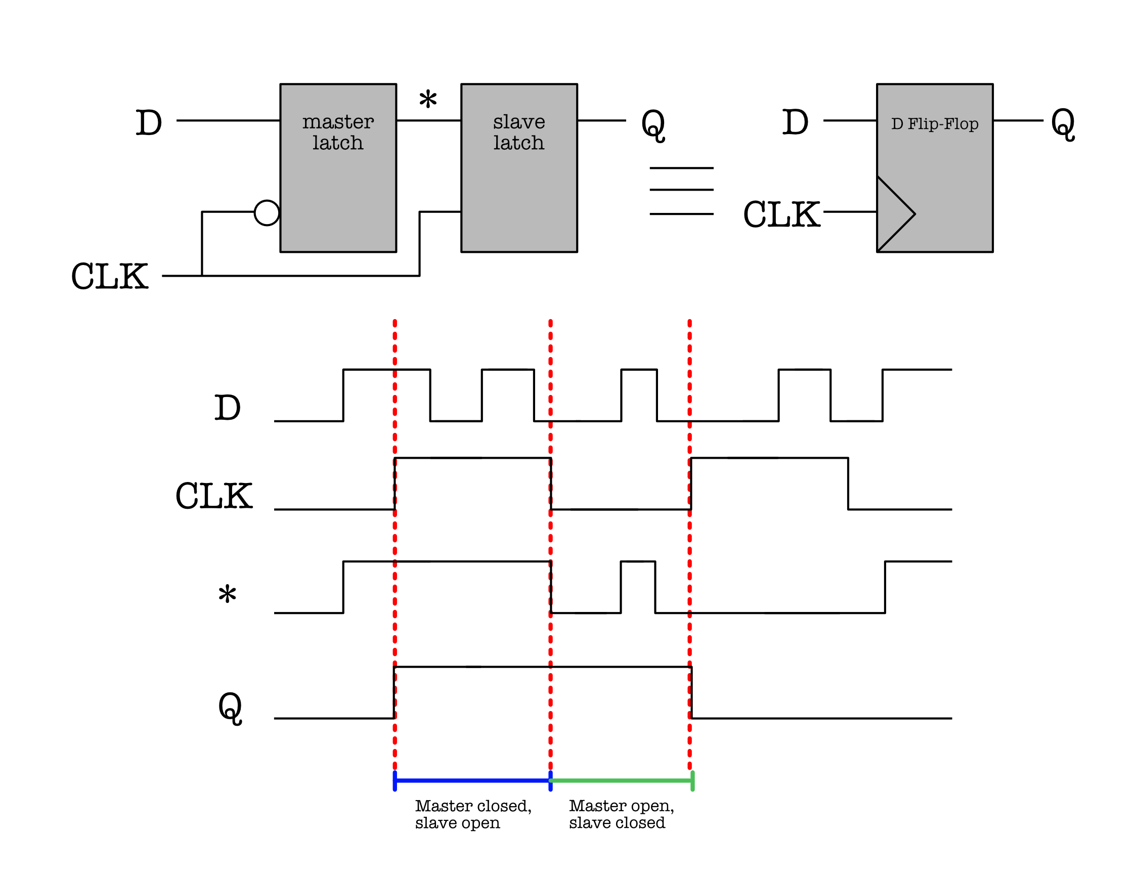
Notice two further behaviors in the Flip-Flop:
-
Unlike the $\star$, the signal at Q is stable throughout an entire clock period, and change only in the next clock period. In comparison, the $\star$ is only stable half the time when the master latch is at memory mode, but reflects ever-changing D-input signal during write mode.
-
The edge-triggered flip-flop in this particular configuration, where the master is the one that receives the inverted CLK signal produces new value at Q (reflects the input at D) at every rising edge of the CLK.
It is as if we are able to capture the instantaneous value of D at each CLK-rise edge, and reflect/produce it at Q for that entire period of the CLK.
You can also make the slave latch to be the one that receives the inverted CLK signal, and the value at Q reflects the input at D at each falling edge of the CLK. Note: The name “edge-triggered” comes from the fact that the output at port Q of the slave changes only when the CLK edge changes (in our case, at every rising edge).
$t_{pd}$ and $t_{cd}$ of Sequential Logic vs Combinational Logic Devices
In the previous chapter, we learned about the definition $t_{CD}$ and $t_{PD}$ for combinational logic (CL) devices, and how to compute these values. For sequential logic (SL) devices, i.e: circuits with Flip-Flops and CLs combined, these timings mean as follows:
-
$t_{CD}$ of a Flip-Flop (or sequential logic devices) is the time taken for an invalid CLK input (not input to the sequential logic circuit), as a result of transition from ‘0’ to ‘1’, to produce an invalid final output of the SL (Sequential Logic) device.
-
$t_{PD}$ of a Flip-Flop (or sequential logic devices) is the time taken for valid ‘1’ CLK input (again, not input to the sequential logic circuit), to produce a valid final output of the SL device.
Note the subtle difference between the $t_{PD}$ and $t_{CD}$ of a combinational vs a sequential device.
To summarise:
-
In combinational device, there is no input CLK and units with feedback paths like the Flip Flops involved. $t_{PD}$ of a combinational device is the time measured from the moment a valid input is fed to the circuit to the moment it produces a valid output of the circuit, and $t_{CD}$ is the time measured from the moment an invalid input is fed to the circuit to the moment it produces an invalid output.
-
However, in SL, our “input” will be the CLK and not the “user” input, and in particular only are concerned with the CLK transition from
0to1, where the D Flip-Flop “captures” a new input value.
Flip-Flop Timing Constraint
Recall that we learned the dynamic discipline that has to be obeyed to ensure that we do not end up storing invalid input signals. In the flip-flop configuration, we connect two D-latches together. Hence the dynamic discipline for the slave latch has to be obeyed by the master latch because the output of the master latch is the input to the slave latch.
To obey the dynamic discipline, there exist this timing constraint for the Flip-Flop configuration:
\[t_{CD_{master}} > t_{H_{slave}}\]Reasons:
-
Imagine the exact moment when the INV CLK seen by master (latch) changes from
0to1, at the same time, the CLK signal seen by slave (latch) changes from1to0. -
This transition by the CLK is not immediate and there is a short time window where the CLK goes from (valid)
1to invalid value to (valid)0. -
This implies that the master goes into write mode while the slave goes into memory mode simultaneously.
-
However, the $\star$ at the output of the master cannot change immediately in order to fulfil the ${t_{H}}$ requirement of the slave.
- The $\star$ has to retain its previous valid value (when the clock was valid) and cannot immediately do the following before the ${t_{H}}$ requirement of the slave is fulfilled:
- Become invalid due to transition in the CLK value, or
- Reflect whatever new input is given at D port of the master latch, even though the master latch is at the write mode.
- This means the contamination delay of the master latch (time taken on signal on $\star$ is be invalid after CLK at G port becomes invalid) has to be larger than the hold time of the slave latch so that the Flip-Flop system obeys the dynamic discipline.
Sequential Logic Device Timing Constraint
The dynamic discipline has to always be obeyed at any part of the sequential logic circuit/device.
Due to this, we have two timing constraints called $t_1$ and $t_2$ that should always apply for any path between two (one upstream and one downstream) connecting Flip-Flops (regardless of how many CLs are there in the middle of the two Flip-Flops) in a SL circuit.
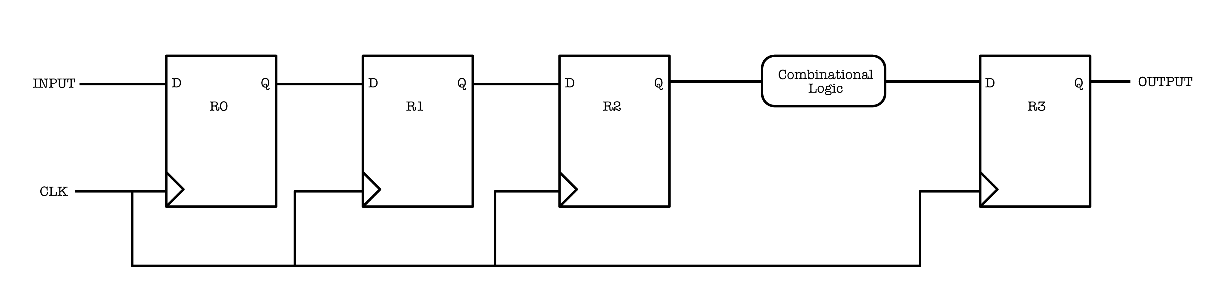
Take into example a very simple combination as shown in the figure below, consisted of two Flip-Flops and one CL device in between. Let’s name the Flip-Flop on the left the “upstream” Flip-Flop and the Flip-Flop on the right the “downstream” Flip-Flop:

If we were to plot the timing diagram of the CLK, output of R1 ($Q_{R1}$), and the output of the CL (CL out), we have the following:
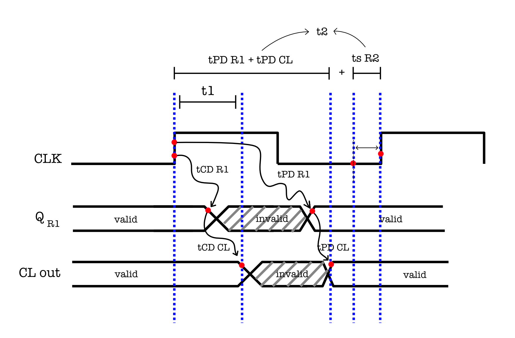
From the diagram above, we can define two timing constraints for this particular scenario:
- $t_1$ : $t_{CD} R_1 + t_{CD} CL \geq t_{H} R_2$
- $t_2$ : $t_{PD} R_1 + t_{PD} CL + t_S R_2 \leq t_{CLK}$
where $t_{CLK}$ is the clock period.
Explanation:
- The $t_1$ constraints ensures that the $t_H$ requirement of the downstream register, R2, is fulfilled by the devices thats put upstream (before it), that is CL and R1 in the example above.
- When the CLK rises at $t_i$, both R1 and R2 are “capturing” different values, simultaneously.
- R1 is receiving current input value at $t_i$, while R2 is receiving the computed old input value that was produced by R1 at $t_{i-1}$.
- The devices upstream of R2 has to help to hold on to this old $t_{i-1}$ values for the $t_H$ of R2 to be fulfilled before responding to the rising edge of the clock and producing new values.
- The $t_2$ constraints ensures that the clock period is long enough for three things to complete:
- Valid signal to be produced at the output of R1 and
- Signal to propagate through CL in between, and
- Signal to be set-up at the downstream register R2 (for memory mode).
- The $t_1$ and $t_2$ requirements must be fulfilled within any paths between two connecting DFFs in a circuit, in order for the overall circuit to obey the dynamic discipline.
We can call the $t_{PD} CL$ (propagation delay of the CL) as the time taken to do actual work or logic computation.
The propagation or contamination delays of a Flip-Flop is not considered a logic computation, because unlike combinational logic devices (that can be made to implement functionalities such as addition, subtraction, boolean expressions, etc), a Flip-Flop does not implement any other special functionalities except to function as a memory device.
See this document to know more about timing computations for sequential logic device.
Synchronization with Input
In any sequential logic circuit we use a single synchronous clock, meaning that we use one same clock to any D Flip-Flop in the device. Our timing constraints ensure that the CLs are given valid and stable input long enough for it to produce meaningful output.
In practice, it is not possible for any arbitrary input to always be synchronised with the clock, i.e: to obey the $t_S$ and $t_H$ requirements (of the external input facing ‘upstream’ DFF) at all times. Recall that dynamic discipline is crucial for any sequential logic circuit to work properly. We are now going to discuss what happens if dynamic discipline is violated.
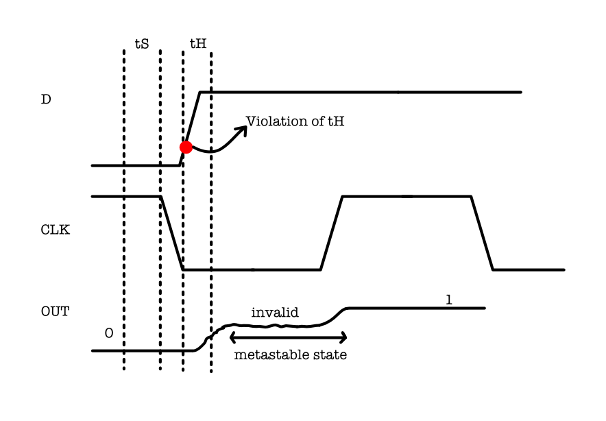
Look at the figure above. Let D be the “user” input to the Flip-Flop and OUT be the output “Q” of the Flip-Flop. When one of the timing constraints ($t_{H}$ in this case) imposed by the dynamic discipline is violated, we may end up storing the invalid values during read/memory mode. This event of storing invalid value is called the metastable state.
The Metastable State
Due to the existence of a feedback loop in the D-latch as shown,
..it has a unique property where there exist a point in its voltage characteristics function whereby Vin = Vout.
We can measure and plot $V_{in}$ (Q’) versus $V_{out}$ (Q) in the D-latch, and come up with a VTC plot as follows:
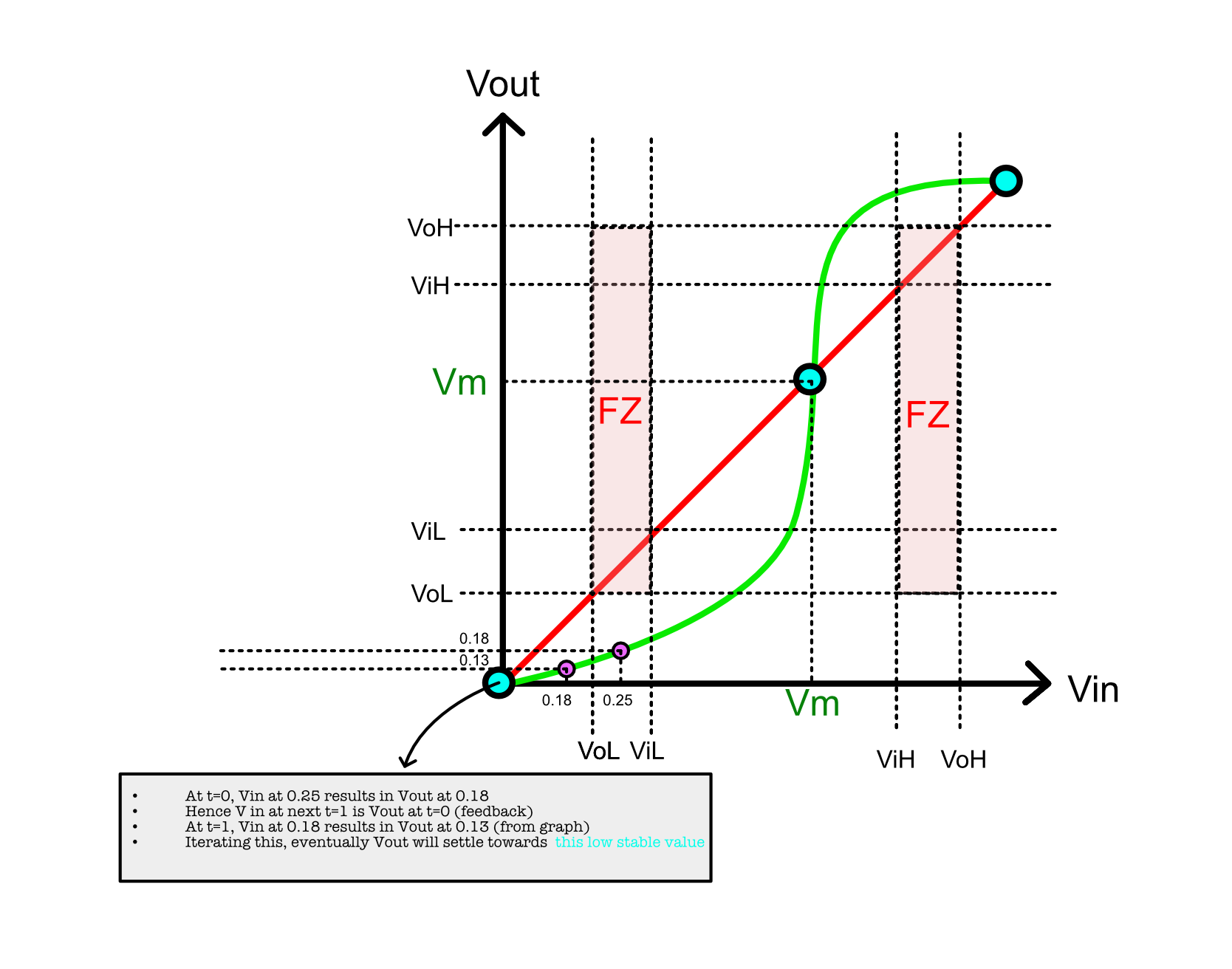
The red line signifies the feedback constraint, where we have Q at $V_{out}$ to be equivalent to Q’ as $V_{in}$. This is the effect of connecting the output of the multiplexer to itself, on the first input port.
The green line signifies the VTC of a “closed latch” state, i.e: when the selector bit of the multiplexer receives a ‘0’ as shown in the diagram above.
Notice that in the closed latch state, the D-latch passes the value from $V_{in}$ (Q’) as the output at $V_{out}$ (Q), and thus we have a shape that resembles that of a buffer.
There are three solutions formed by the intersections of the red line (feedback constraint) and the green line (VTC of the closed latch), as indicated by the three circles in the figure above: two end points that results in “valid” voltages (either 0 or 1), and one middle point that is metastable (denoted as $V_m$).
What is the meaning of these solutions? Well, we are indeed creating a device which output is connected back as its input, so we need to know where the system will tend towards.
Let’s think about this particular scenario while looking at the VTC plot above:
-
If the initial $V_{in}$ value is well below $V_m$, then it will produce an even lower $V_{out}$.
- This $V_{out}$ becomes a new $V_{in_2}$ when the signal traverse the loop for the second time, and produce another even lower $V_{out_2}$.
- Eventually, the value of $V_{out_N}$ after certain N loops traversal tends towards the stable low indicated by the teal circle on the left.
-
In summary, during each loop $i$, $V_{out_i}$ produced is always less than $V_{in_i}$, and thus after a few loops, the final value of $V_{out}$ tends towards the teal point of the left.
The little note at the figure above illustrates this scenario too.
Otherwise, if the initial value of $V_{in}$ is well above $V_m$, then the opposite applies and the final value of $V_{out}$ after N loops will tend towards the stable high indicated by the teal circle on the right, since $V_{out_i}$ is always greater than $V_{in_i}$ at each loop $i$.
However, if we have $V_{in} = V_m$, then from the graph we can easily see that $V_{out}$ will again be at equivalent value, at $V_m$ in the following loop traversal. This $V_{out} = V_m$ will be an input back at $V_{in}$ (in the next loop), which will produce $V_m$ again over and over (perpetually) under ideal, noise-free case.
Therefore, without the presence of noise or external disturbances, if $V_in$ is exactly at $V_m$ then there is always a chance that we could wait forever for it to be able to settle to either a stable values. A small presence of noise will drive $V_{in}$ down or up and eventually it may settle to a stable value, however this is not guaranteed in bounded time.
The state whereby your SL device is unable to settle to a stable / valid value for unknown period of time is called the metastable state. Obviously we do not want this because the output of the device is invalid during this unknown time frame, and therefore rendered useless.
In summary, properties of metastable state are illustrated below:
-
It corresponds to an invalid logic level – the switching threshold of a device
- It is an unstable equilibrium, a small noise/pertubation may cause it to accelerate towards either ends: a stable
0or1… eventually (but it might not too). - Depending on how close $V_{in}$ is to $V_m$ and presence of noise, it also may take forever to settle towards a stable value (unbounded time).
- Every bistable system exhibits at least one metastable state.
Hence, the metastable state is an inevitable risk of synchronization because our active device always have a fixed-point voltage $V_m$ such that $V_{in} = V_m$ implies $V_{out} = V_m$, caused inherently by the feedback loop constraint and the VTC of the multiplexer.
The violation of dynamic discipline may put our feedback loop at some voltage near $V_m$. The time taken for $V_{out}$ to eventually settle towards a stable 0 or 1 is inversely proportional to current $|V_{out} - V_m|$, and is theoretically infinite for $V_{out} = V_m$.
Since there is no lower bound on $|V_{out} - V_m|$, then there is no upper bound for the settling time of eventual $V_{out}$ value.
In other words, we cannot completely avoid the metastable state.
If an SL device enters the metastable state, it might eventually settle to a valid zero… or a valid one, but there is no guarantee when this will happen. It may take a second, or it may take forever to settle.
Note that this comes at the cost of responsiveness of the device.
Summary
As stated above, a sequential logic device has a general structure as shown below:
During each clock period, it should be able to compute the next value (next state), and output value. The output at any point in time, is always affected by the current state, which is the state computed in the previous clock period / time step. Hence the name sequential logic comes from the fact that it is a type of logic circuit whose output depends not only on the present value of its input signals but on the sequence of past inputs, (the input history) as well.