 Computation Structures
- Logic Synthesis
50.002 Computation Structures
Information Systems Technology and Design
Singapore University of Technology and Design
Logic Synthesis
Overview
The purpose of creating combinational devices is to synthesise logic, meaning that we create a device that is able to give a certain combination of output given a certain combination input. In other words, a device that adheres to a truth table, i.e: its functional specification.
Any combinational device has to have a functional specification. Functional specifications are represented with truth tables. So for example, the following is the truth table of an NAND gate (input: A and B, output: Y):
\[\begin{matrix} A & B & Y\\ \hline 0 & 0 & 1\\ 0 & 1 & 1\\ 1 & 0 & 1\\ 1 & 1 & 0\\ \end{matrix}\]The truth table for an AND gate is the opposite (input: A and B, output: Y):
\[\begin{matrix} A & B & Y\\ \hline 0 & 0 & 0\\ 0 & 1 & 0\\ 1 & 0 & 0\\ 1 & 1 & 1\\ \end{matrix}\]So as you can see, “NAND” is just a short for “not-an-and”. The output of a NAND gate is always 1 unless both A and B are 1. The output of an AND gate is the opposite, that is it is always 0 unless both A and B are 1.
N-input Gates
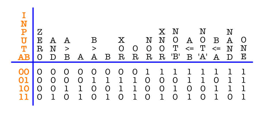
There are 16-possible 2-input gates, as shown in the image below. The AND gate and the NAND gate are among the few ones that are more common. The OR, NOR, XOR, and XNOR gates are very commonly used too. In short, there are $2^{2^x}$ possible x-input gates, but not all are exactly useful in practice.
Note: please do not memorize these things blindly. They’re logic, encoded in binary. The names of the gates signify the logic, for example logic AND means that we shall detect and produce a discernible output if input
iandj(or any other inputs) to the device are all1.
Sum of Products
We can also have functional specifications in terms of boolean expression. To convert truth tables into boolean expressions, we take the following steps:
- Look only for the rows with output= 1. In the case of the NAND gate, we look at row 1, 2, and 3.
-
For each row in with output = 1, if the value of the input is a 0, then express it with a NOT.
Taking the NAND gate’s truth table as example,
- For row 1 of NAND gate’s truth table, we have $\overline{A} \text{ } \overline{B}$.
- For row 2, we have $\overline{A}B$.
- For row 3 we have $A\overline{B}$.
- Sum all the expressions from the rows with Y=1.
Taking the NAND gate’s truth table as example, the sum of product is: \(\begin{aligned} Y = \overline{A} \text{ } \overline{B} + \overline{A}B + A\overline{B} \end{aligned}\)
- The expression above is called the sum of products.
Sometimes in textbooks, it is called as canonical sum of products. They mean the same thing as just “sum of products”.
Universal Gates
NAND and NOR gates are universal, meaning that each alone can implement any boolean function. AND, OR, and INV alone aren’t sufficient, but together these three can express any boolean expressions (we will see this in the next section).
We can use just NANDs or just NORs gates to make AND, OR and INV gates:
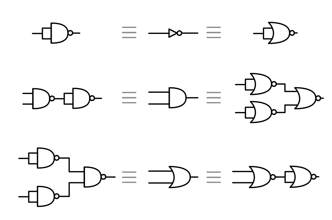
Therefore, NANDs and NORs are universal gates.
Straightforward Logic Synthesis
Recall that the goal of combinational devices is that they are created to adhere to a certain functional specification. We can make various logic gates and combine them to synthesize a more complex logic or truth table. However, there are basic logics that can be used to synthesize any kinds of other (more complex) logic. These are: INV (inverter), AND gate, and OR gate.
The truth table for OR gate is as follows, that is the output is 1 if either A or B input is 1:
\(\begin{matrix}
A & B & Y\\
\hline
0 & 0 & 0\\
0 & 1 & 1\\
1 & 0 & 1\\
1 & 1 & 1\\
\end{matrix}\)
Given a sum-of-products boolean expression, we can make a combinational device that has that boolean expression as functional specification using these three types of logics: INV, AND, and OR with arbitrary number of inputs.
For example, given the following sum of products expression,
\[\begin{aligned} Y = \overline{C} \text{ }\overline{B} A + \overline{C} B A + CB\overline{A} + CBA \end{aligned}\]We can make a combinational device as such that it adheres to the expression above using these three logic devices only, as shown below:
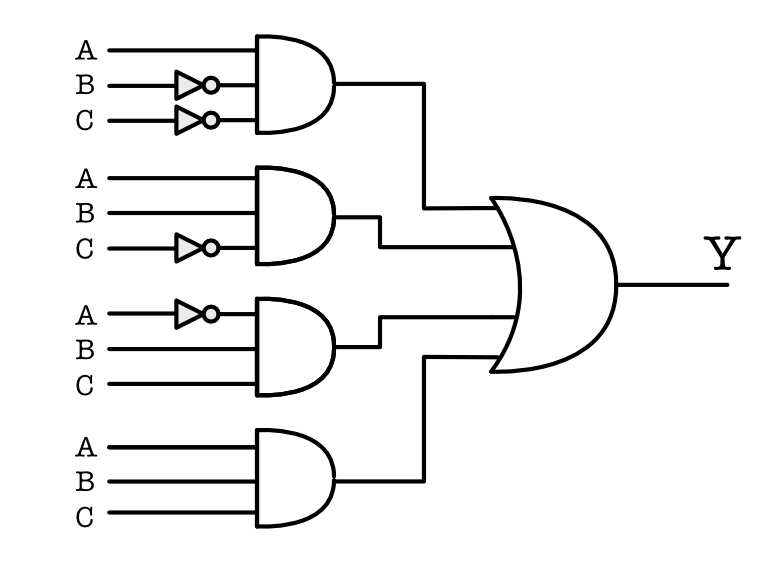
Explanation:
- The boolean expression of the output Y contains 4 terms that are added or summed together.
- The 4-input OR gate at the output Y represents the summation of these four terms.
- The AND gates in the second “column” of the figure represents the combination of each of the input terms,
For example: $\overline{C} \text{ }\overline{B} A$ means not C, not B, and A combined together as an input to a 3-input AND gate.
- The INV at the input represents the NOT inputs (negated inputs).
Using these steps, we can come up with the simplest (not necessarily the most efficient, cheapest, smallest, etc), most straightforward logic synthesis.
Notice that if the expression contains many terms summed together, we need bigger OR gate at the output. This causes the size of our device to be bigger, and therefore more expensive. In the later sections, we learn how to reduce the boolean expression such that we have less number of terms, and thus are able to synthesize the logic more effectively.
Boolean Algebra Properties
Another tool we need to master before being able to minimise or reduce boolean expression is boolean algebra properties. They are useful to manipulate boolean expressions so that we quations. A summary end up with simpler terms and reduce the terms, while still keeping the logic equivalent.
Here are the simpler boolean algebra properties that we must know before proceeding to a more complex ones:
\[\begin{aligned} \text{OR rules: } & a+1 = 1, \\ & a+0 = a, \\ & a+a=a\\ \text{AND rules: } & a1=a, \\ & a0=0, \\ & aa=a\\ \text{COMPLEMENT rules: } & a + \bar{a}=1, \\ & a\bar{a}=0 \\ \end{aligned}\]Below are more laws that are built based on some of the rules above and each other. We do not have to prove each law in this course, but if you’re interested, you can look for other references such as here.
\[\begin{aligned} \text{Commutative law: } & a+b = b+a, \\ &ab = ba\\\\ \text{Associative law: } & (a+b)+c = a+(b+c),\\ & (ab)c = a(bc)\\\\ \text{Distributive law: } & a(b+c) = ab+ac, \text{ --- OR distributive},\\ & a+bc = (a+b)(a+c) \text{ --- AND distributive} \end{aligned}\]The two laws below are useful to perform boolean minimisation because we might end up with less number of terms while keeping the same logic:
\[\begin{aligned} \text{Absorption law: } & a+ab=a, \\ & a+\bar{a}b = a+b,\\ &a(a+b) = a, \\ &a(\bar{a}+b) = ab\\ \text{Reduction law: } &ab + \bar{a}b = b, \\& (a+b)(\bar{a}+b) = b \end{aligned}\]Note that the boolean algebra properties above also applies for the inverted form, e.g: if $\bar{a}$ is swapped with $a$ instead:
- $a+\bar{a}b = a+b$ (original); $\bar{a}+ab = \bar{a}+b$ (invert $a$)
- $ab + \bar{a}b = b$ (original); $a\bar{b} + \bar{a}\bar{b} = \bar{b}$ (invert $b$)
- $a(a+b) = a$ (original); $\bar{a}(\bar{a}+\bar{b}) = \bar{a}$ (invert both)
There’s a lot of boolean theorems that are derived from the above, for example:
\[\text{Consensus Theorem: } ab + \bar{a}c + bc = ab + \bar{a}c\]Proof:
\[\begin{aligned} ab + \bar{a}c + bc &= ab + \bar{a}c + (\bar{a}+a)bc\\ &=ab + abc+ \bar{a}c + \bar{a}bc \\ &= ab(1+c) + \bar{a}c (1+b)\\ &=ab + \bar{a}c\ \end{aligned}\]What’s important is to pay attention to the relationship between each variables. You can easily let $\bar{a} = x$ and find the formula applies as well for the inverted version.
DeMorgan’s Theorem
Finally, the DeMorgan’s theorem is useful as a tool for us to manipulate boolean equations as it converts between OR to AND and vice versa using INV. The Theorem states:
\[\begin{aligned} \overline{a+b} &= \overline{a} \text{ } \overline{b}\\ \overline{ab} &= \overline{a} + \overline{b} \end{aligned}\]Boolean Minimization Example
When given a boolean expression, we need to be creative and utilize all properties of boolean algebra to minimise the expression. For example, we can use the reduction rule from the boolen algebra cheat-sheet above to perform boolean minimization:
\[\begin{aligned} Y &= \overline{C} \text{ }\overline{B} A + \overline{C} B A + CB\overline{A} + CBA\\ &= \overline{C} \text{ } \overline{B} A + \overline{C} BA + CB \text{ (reduce the last two terms)}\\ &= \overline{C} A + CB \text{ (reduce the ist two terms)} \end{aligned}\]Karnaugh Map for Boolean Minimisation
The Karnaugh Map offers an alternative method to perform boolean minimization. This is a method to easily perform boolean minimization, and ultimately the end goal is to reduce the digital circuit to its minimum number of gates (save cost and save space).
The following figure shows a 2-input (by input it just basically means how many input boolean variables), 3-input, and 4-input Karnaugh maps. Please do not change the order, they follow Gray code configuration to preserve adjacency so rules 1-6 below can apply.
It is possible to rotate them clockwise or anticlockwise but do so only if you understand the logic behind arrangement of Karnaugh map configuration, which is out of this syllabus.
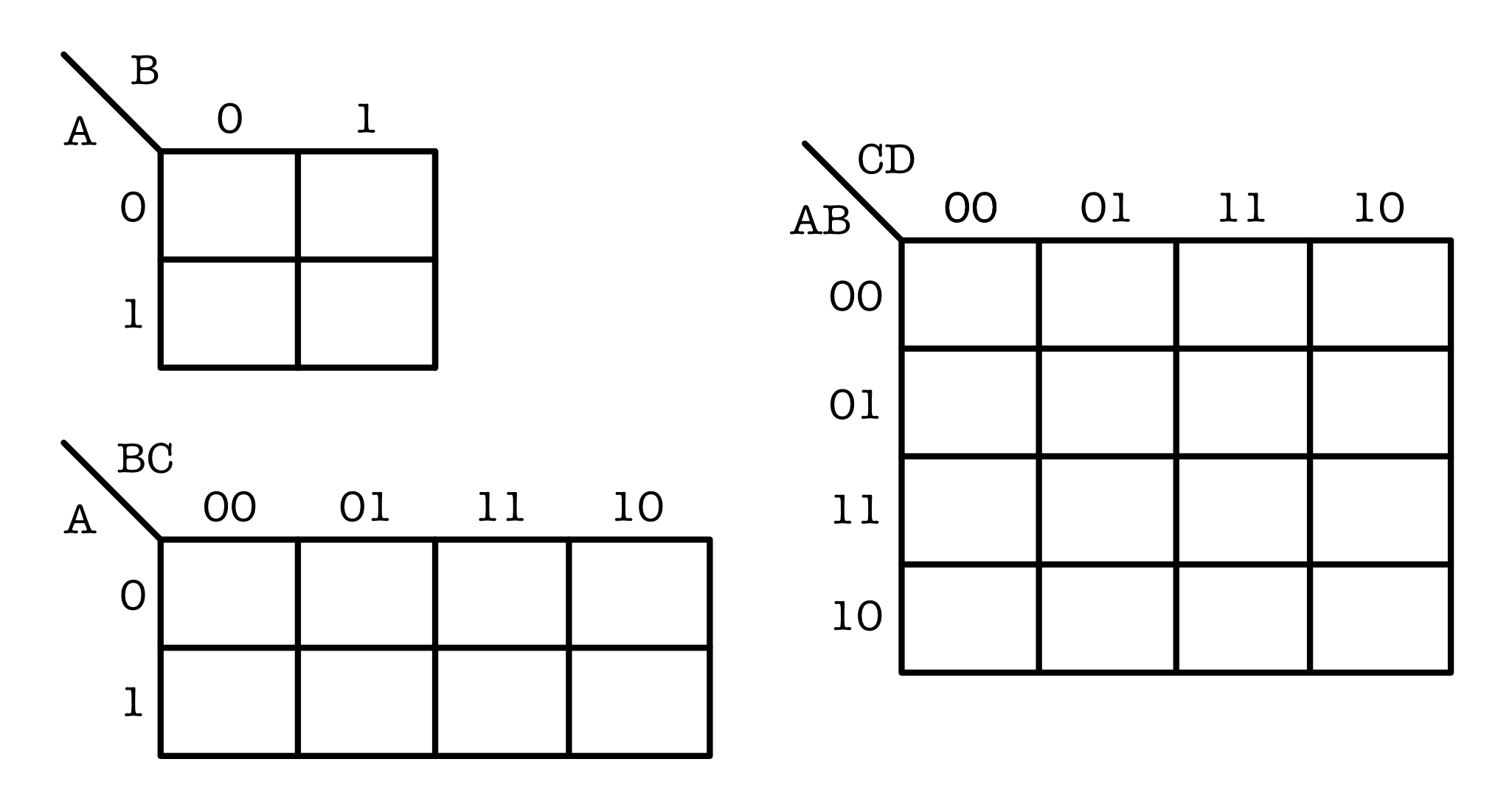
The number of cells of Karnaugh maps with $x$ inputs is $2^x$ cells. Then, fill in ‘1’ to all the cells that represent logic ‘1’ on the boolean expression.
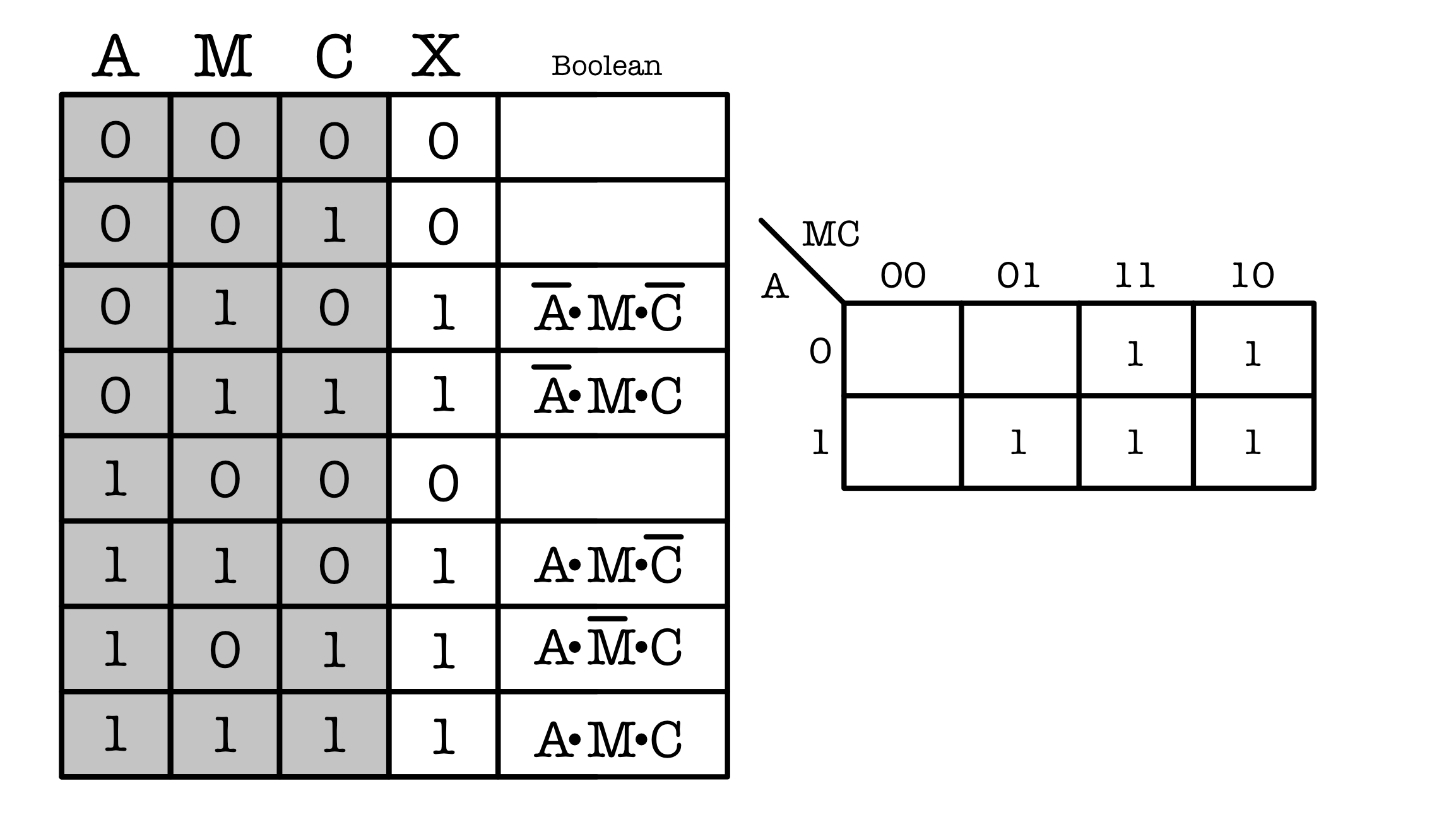
For instance, here is an example of a truth table and its corresponding Karnaugh map:
Then you can simplify the Karnaugh Map using these 6 ground rules:
- Groups should contain as many ‘1’ cells (i.e. cells containing a logic 1) as possible and no blank cells.
- Groups can only contain 1, 2, 4, 8, 16 or 32… etc. cells (powers of 2).
- A ‘1’ cell can only be grouped with adjacent ‘1’ cells that are immediately above, below, left or right of that cell.
- No diagonal grouping
- Groups of ‘1’ cells can overlap.
- This helps make smaller groups as large as possible, which is an advantage in finding the simplest solution.
- The top/bottom and left/right edges, and also the 4 corners of the map are considered to be continuous.
- Larger groups can be made by grouping cells across the top and bottom or left and right edges of the map:
- Top row and bottom row (or parts of them) can form one group as long as condition 1-4 are satisfied.
- Leftmost column and rightmost column (or parts of them) can also form one group as long as condition 1-4 are satisfied.
- There should be as few groups as possible.
Following the rules above, the simplified example Karnaugh map is:
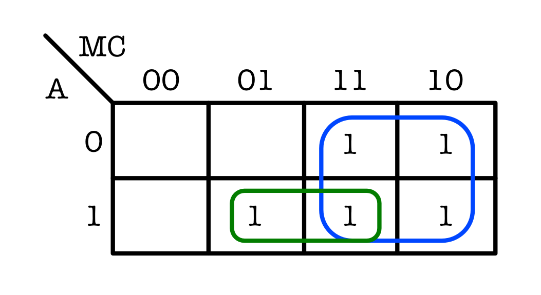
To convert this Map back into boolean expression, we need to look at each group and use a little bit of logic:
-
In the blue group, the output is
1regardless of A, and regardless of C. Hence, the boolean expression for the blue group is just M. -
In the green group, the output is
1regardless of M. Therefore, the boolean expression for the green group is AC. -
The complete simplified boolean expression is: X = M + AC.
X = M + AC is logically equivalent to X = $\bar{A}M\bar{C}$+$\bar{A}MC$+ $AM\bar{C}$+$A\bar{M}C$+$AMC$ (the sum of products of its truth table).
You can also obtain the minimized expression using boolean algebra:
- Reduction rule: $\bar{A}M\bar{C}$+$\bar{A}MC$ = $\bar{A}M$
- Reduction rule: $AM\bar{C}$+$AMC$ = $AM$
- So far we have: X = $AM+ \bar{A}M+AM\bar{M}{C}$
- We can further reduce the first two terms, resulting in X = $M+A\bar{M}{C}$
- Use absorption rule to absorb $\bar{M}$, we end up with X = $M+AC$
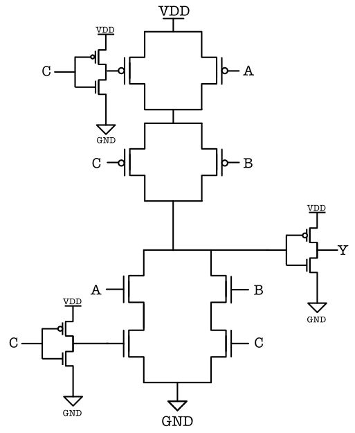
Logic Synthesization with CMOS
We can create a combinational logic device easily given the minimized boolean expression, using any of the universal gates:
- NANDs only
- NORs only
- AND, INV, and OR
Each gate can be created using transistors: PFETs and NFETs arranged in a complementary way. The schematic of each is as follows:
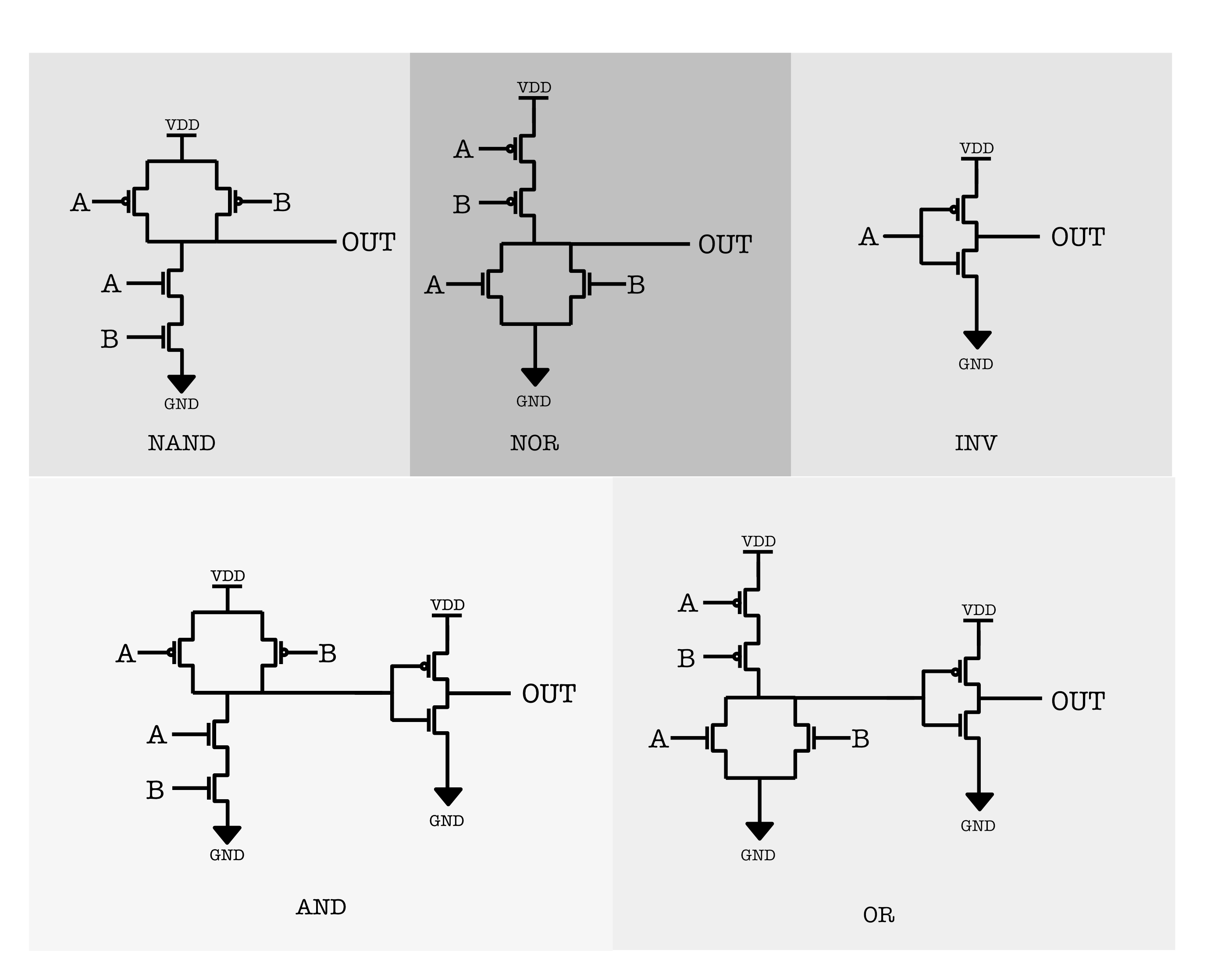
The OR and AND gates are simply the NOR and NAND gates with inverter at the output.
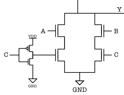
We can also create the device straight using CMOS recipe given the minimised boolean expression (instead of using the universal gates). For example, given this minimised equation that we did earlier: \(Y= \overline{C} A + CB\)
It can be made this way with a combination of universal gates:
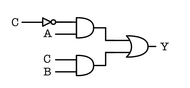
This requires 20 MOSFETs to build.
Or the primitive way:
- Step 1: Construct a pull-down circuitry:
- for each ‘+’ (OR) we build a parallel NFET circuit
- for each $\cdot$ (AND) we build a series NFET circuit
Therefore we have two sets of two NFETs in series:
- Step 2: Add inverter at the output.
- In Step 1 we created a pull-down circuitry that is activated when each of the terms in the boolean expression produces an overall ‘1’.
E.g: when $B, C$ are both 1, the pull-down is activated as current can flow from $Y$ to the GND. The effective output at $Y$ will be then
0when $B,C$ are both1. - Since what we want is the opposite, we need to put an inverter at the output.
that is $Y=1$ when $B,C$ are both 1, we need to put an inverter at the output, as shown:
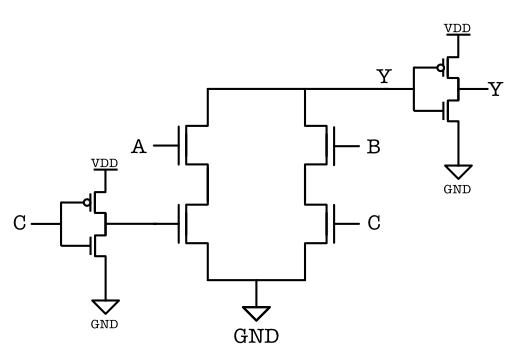 If what you want is for $Y$ to be
0when $B,C$ are both1then there's no need to put an inverter in the end. Just draw the complementary pullup and call it a day
- In Step 1 we created a pull-down circuitry that is activated when each of the terms in the boolean expression produces an overall ‘1’.
- Step 3: Construct the complementary pull-up circuitry and assemble.
Refer to the CMOS recipe in the previous chapter.
This requires 14 MOSFETs to build, less than the previous design. It is definitely easier (for us) to create a combinational logic device using a bunch of universal gates, but it comes at the cost of money and size.
Note that the CMOS recipes that we learn in this course also does not guarantee that you can build a device with minimised number of transistors, given its functional specification. It is an art to create the most efficient circuit in terms of money, size, and usage.
Special Combinational Logic Devices
The Multiplexer
The Multiplexer (shorted as “mux”) is a special combinational logic device that is very commonly used in practice. It is implemented using basic logic gates (INV, AND, and OR, or NANDs). The mux is expensive to manufacture, but universal, meaning that it can implement any boolean function because essentially it “hardcodes” the truth table.
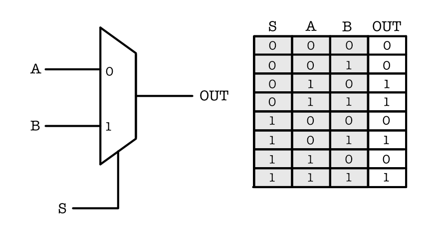
The symbol for a mux is as shown in the image below. The truth table is written at the side. A mux always has three types of terminals:
- $2^k$ bits data inputs,
kbits selector signal(s) –this is also an input, but we have a special name for them them: selector– , and- 1-bit output.
It’s functioncomponents: the inputs, the selector signal(s), and the output. It basically “allows” oneeither of the input signals to be reflected at OUTpass through when selected.
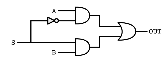
For example in the case of 2-input mux below, when S=0, it will reflect whatever value the signal $A$ carries (1 or 0) as its output:
Take some time to make sense of the truth table. That is if S=0, OUT = A. Else, if S=1, OUT = B. produce the signal $D_0$ as its output:
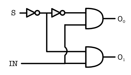
You can build a 2-input multiplexer using basic gates:
Some properties about multiplexers:
- Muxes are universal, meaning that it can implement any boolean functions
- A Mux can have $2^k$ data inputs, and $k$ bits select inputs, and only can have 1 output terminal.
We can also generalise the multiplexer to take more inputs: 4, or 8, or 16, etc. We can either build a bigger multiplexer or cascade many 2-input multiplexers. The following figure shows an example of a 4-input multiplexer, implemented as a big mux (left) or using a series of 2-input mux (right):
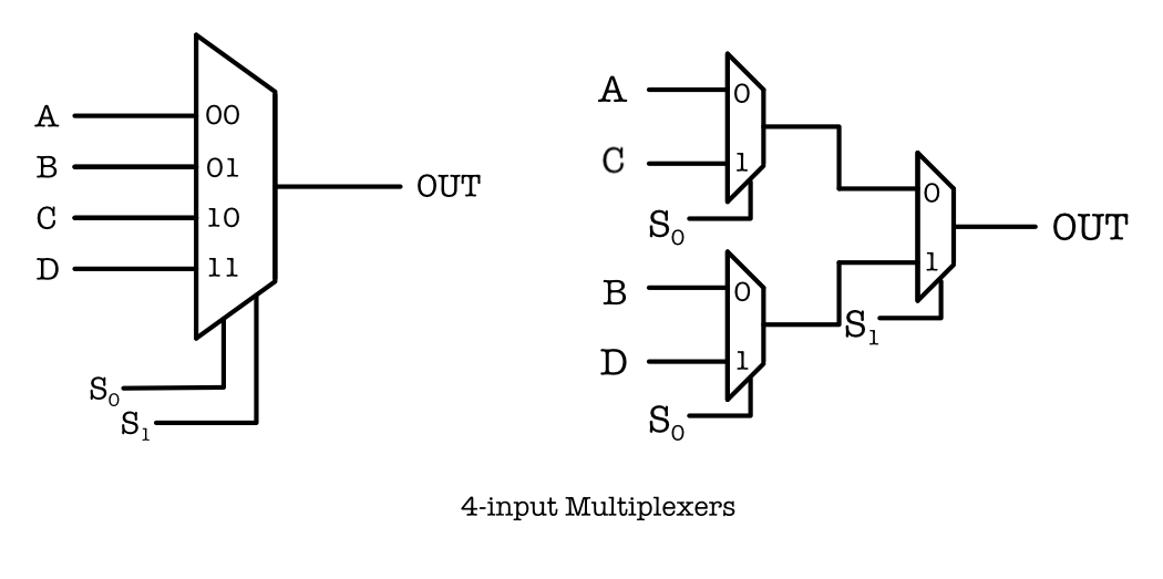
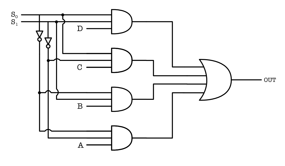
Similarly, you can build a 4-input mux using basic logic gates:
Below is an example of how a mux can be used to implement a more complex combinational device, the full adder that we encounter in the lab. The truth table of a full adder is as shown, it is basically an addition (of three inputs) in base 2:
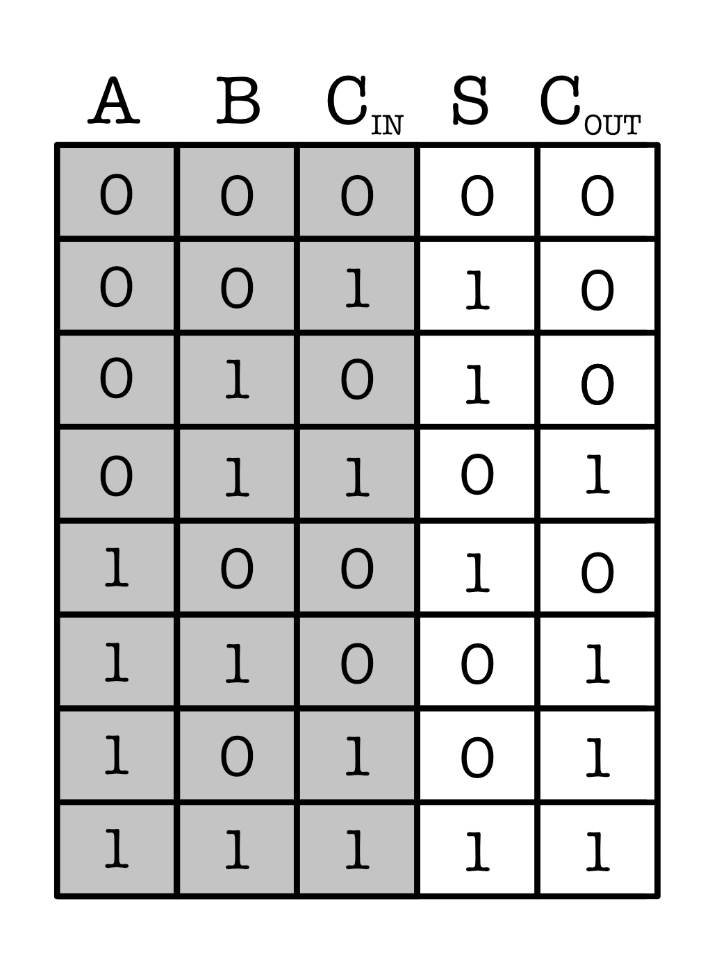
The multiplexer can simply implement the truth table by mapping each type of output bit $C_{out}$, and $S$ in each of the input terminals of the mux as illustrated below (for the carry out):
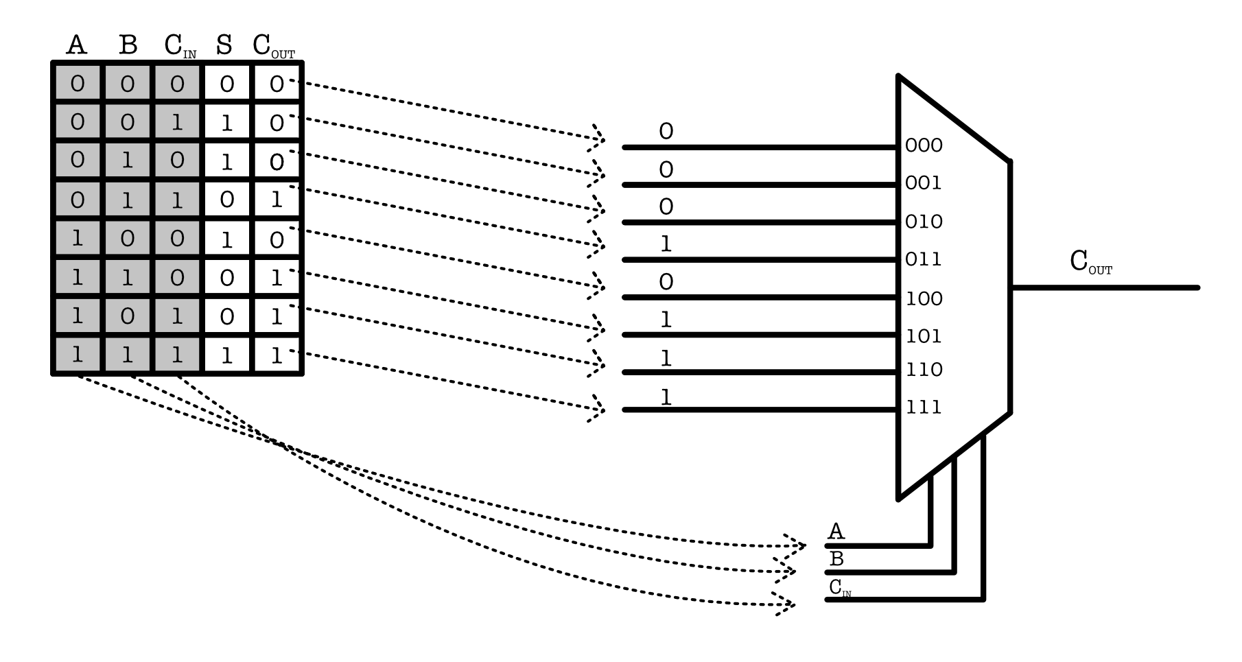
We can do the same thing for $S$, and both of them combined will function as a full adder.
Decoder
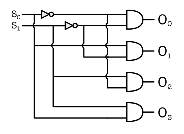
The Decoder (also known as “demux”) is a special combinational logic device that is also very commonly used in practice. It can have $k$ select inputs, and $2^k$ possible output combinations. The schematic of a 1-select input decoder is:
Practice: Draw out the truth table of the decoder above.
The schematic of a 2-select inputs decoder: $S_0$ and $S_1$ is (we omit the “IN”) because it is usually just VDD:
Take some time to trace out the selector values to the output and draw out a truth table for the decoder.
Note: do not worry about the logic gate schematics of a decoder. It is only there to show you that a decoder is made up of the normal logic gates like inverters and AND gates.
Some properties about decoders:
- A Decoder is basically the opposite of a multiplexer. It has $k$ select inputs, and $2^k$ possible data outputs, and only 1 bit of input (typically VDD). The symbol is shown below:

- This figure omits the 1 bit input to the decoder because it is always set to 1 in practice.
- Therefore, for a 4 bit decoder as shown in the figure above, the input signals are only the two SELECTOR signals, denoted as $IA_0$ and $IA_1$ in the figure.
-
At any given time only 1 bit of the $2^k$ output bits can be
\[\begin{matrix} S & O_1 & O_2\\ \hline 0 & 1 & 0 \\ 1 & 0 & 1\\ \hline \end{matrix}\]1(high). This is apparent when we try to draw the truth table for a $k$ input decoder. For example, the truth table for a 1-selector bit decoder is:The truth table for a 2-selector bits decoder is:
\[\begin{matrix} S_0 & S_1 & O_0 & O_1 & O_2 & O_3\\ \hline 0 & 0 & 1 & 0 & 0 & 0 \\ 0 & 1 & 0 & 1 & 0 & 0 \\ 1 & 0 & 0 & 0 & 1 & 0 \\ 1 & 1 & 0 & 0 & 0 & 1 \\ \hline \end{matrix}\]In other words, only the selected output $i$ is HIGH (
1), and the rest of the $2^k-1$ data output is LOW (0).
Read-Only-Memories (ROM)
One of the application of a decoder is to create a read-only-memories (ROM).
You can buy them online, like this product.
For example, if we “hard-code” the Full-Adder using a decoder, we end up with the following schematic:

Explanation for the schematic above:
-
At the output of the decoder, the little circuit with inverted triangle symbol signifies a pulldown circuit (an NFET connected to ground), which will “drain” a signal into LOW (0).
- Recall that at each combination of select signal $A, B$, and $C_i$, only one of the 8 outputs of the decoder will be
1.- For example, when $A=0, B=0, C_{in}=1$, the second output line of the decoder from the top is
1:
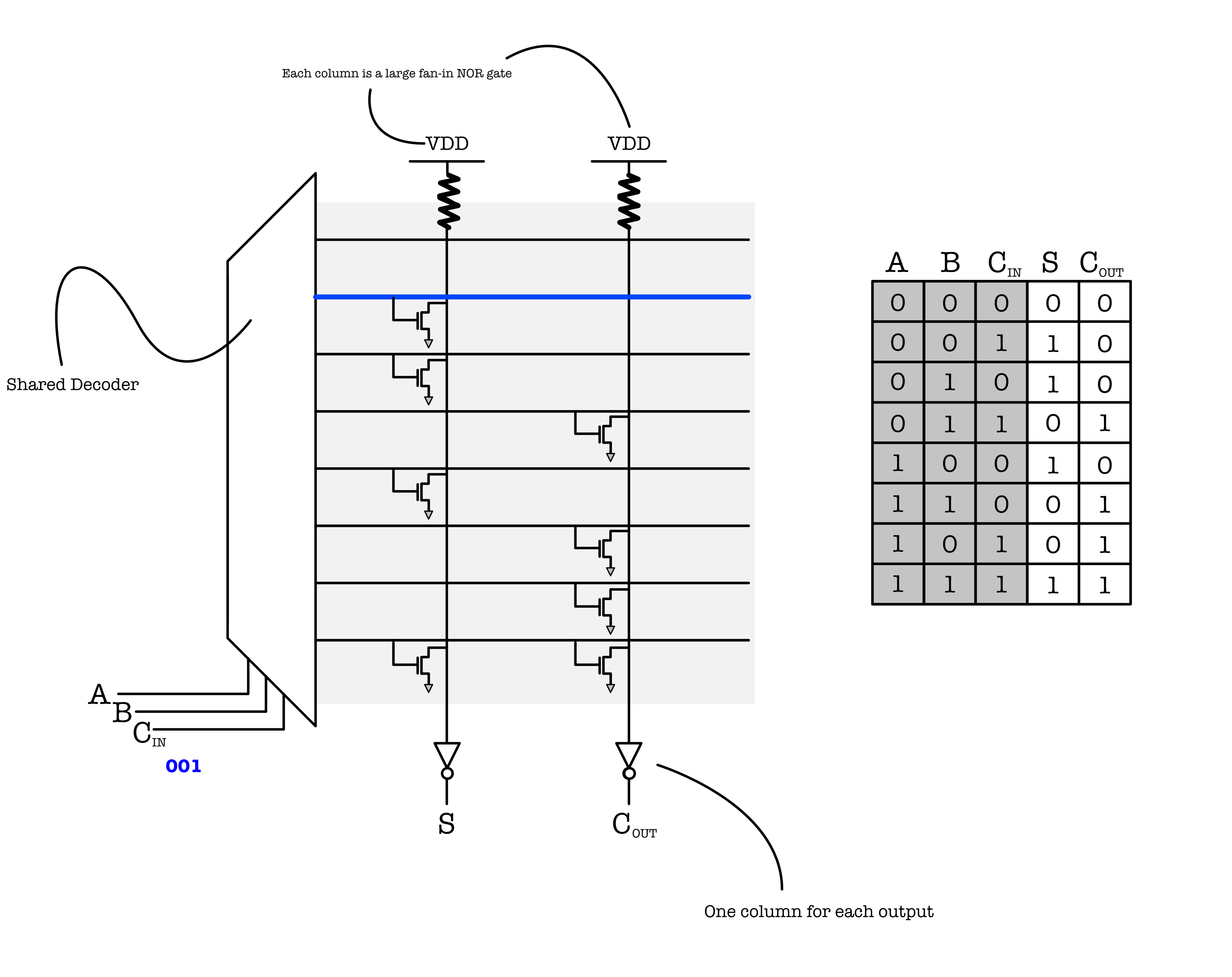
- There’s a pulldown at the S line, which drains the
VDDand results in0at S line towards the inverter. There’s no pulldown for the $C_{out}$ line, so the value fed in towards the inverter in the $C_{out}$ line is1> - There’s a pulldown for S (it is connected to the ground), which makes it 0, and no pulldown for the $C_{out}$, which makes it 1. - Therefore, when $A=0, B=0, C_i=1$, $S=0$ and $C_{out}$ is 1.
- For example, when $A=0, B=0, C_{in}=1$, the second output line of the decoder from the top is
-
Note the presence of inverters by invention at the end of the two vertical output lines for $S$ and $C_{out}$, so the overall output is inverted to be
1for $S$S and0for $C_{out}$. -
By invention, the location of the “pulldown” circuits correspond to a ‘1’ in the truth table for that particular output ($S$ or $C_{out}$).
- For $K$ inputs, decoder produces $2^K$ signals, only
1which is asserted (valid “High”, or simply “selected”) at a time.
The properties of ROM are as follows:
- ROMs ignore the structure of combinational functions (our truth table is “hardcoded”.
- The selectors are like addresses of an entry.
- For an $N$-input boolean function, the size of ROM is roughly $2^N \times \text{ #outputs}$.
For example, the Full Adder has 3 inputs (A, B, $C_{in}$), and 2 outputs (S and $C_{out}$). Hence the size of the ROM is $2^3 * 2 = 16$.
Conclusion
Synthesizing combinational logic is not a simple task. There are many ways to realise a functionality, i.e: the logic (that the device should implement) represented by the truth table or boolean expression. We can use universal gates (only NANDS, or only NORS), a combination of gates (INV, AND, and OR), or many other ways (multiplexers, ROMs, etc).
Of course “hardcoding” a truth table using ROM and Multiplexers are convenient, because we do not need to think about simplifyfing the boolean expression of our truth table (which can get really difficult and complicated when the truth table is large, i.e: complicated functionality). However it comes at a cost: the cost of the materials to build the ROM / Multiplexers, and at the cost of space (we need use a lot of logic gates to build these).