 Computation Structures
- Designing an Instruction Set
50.002 Computation Structures
Information Systems Technology and Design
Singapore University of Technology and Design
Designing an Instruction Set
Overview
To create a programmable control system suitable for general purposes (like the Universal Turing Machine), we need to define a set of instructions for that system, such that it is able to support a rich repertoire of operations.
We can create a machine that is simply programmable, but it also has to support the following features for it to resemble the Universal Turing Machine:
- An expandable memory unit (to represent that infinite tape)
- A rich repertoire of operations
- Ability to generate a new program and then execute it
In this document, we will begin by understanding what does it mean to simply create a (basic) programmable machine, and how the current general-purpose computer model is both programmable and possess these three features.
An Example of a Basic Programmable Control System
Suppose we have a simple sequential logic circuit called Machine $M$ as shown below. It receives one $N$ bit input, and produces two output: $N$ bit output1 and 1 bit output2. Formally, we call this “circuit” a datapath. A datapath is a collection of functional units made up of combinational devices, registers, and buses.
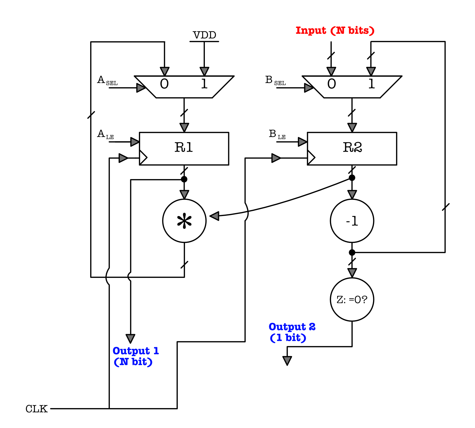
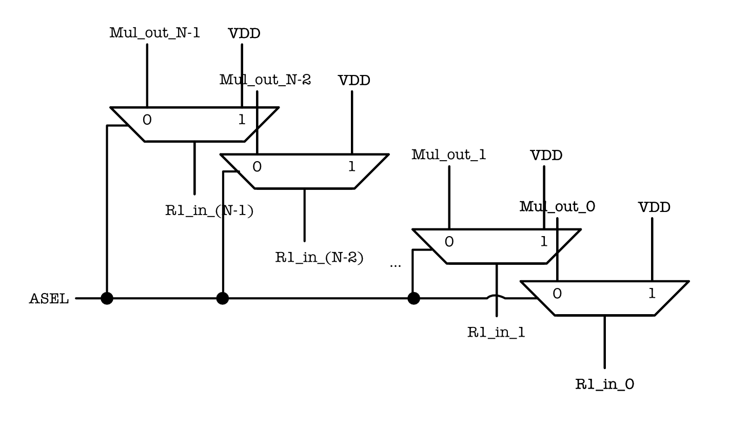
Note that since the machine receives $N$ bit inputs, it means that there are $N$ units of each 2-to-1 multiplexers in parallel, as shown:
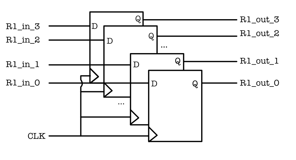
The registers also are actually N 1-bit registers:
In diagrams, they are only drawn once, but you can differentiate between a single wire (that carries 1-bit of information) with a bunch of wires that carry $>1$ bits of information by the “/” symbol.
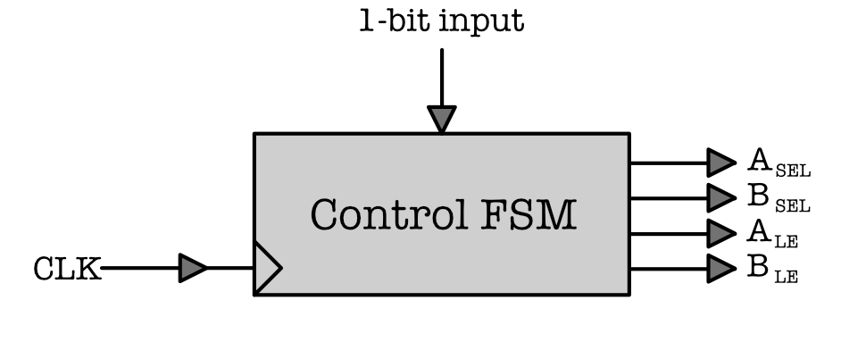
In this example, Machine $M$ also has four control signals, symbolised as $\text{A}{\text{SEL}}$, $\text{B}{\text{SEL}}$, $\text{A}{\text{LE}}$, and $\text{B}{\text{LE}}$. These four control signals are dictated by a control FSM unit shown below, meaning that these four signals will vary accordingly at each time step, hence changing the behaviour of the circuit above when we need it:
Other notable components of $M$:
- A decrement unit symbolised as
-1 - Computation of
z = (input == 0) ? 1 : 0 - A multiplier unit symbolised as
*
In other words, we can control the processing of inputs at each time-step (clock cycle) with a (plugged in) Control FSM unit.
If we can load another Control FSM unit that also produces these four signals but in different sequences, then we allow machine $M$ to be programmable. The complete circuit after plugging in a Control FSM unit is as shown:
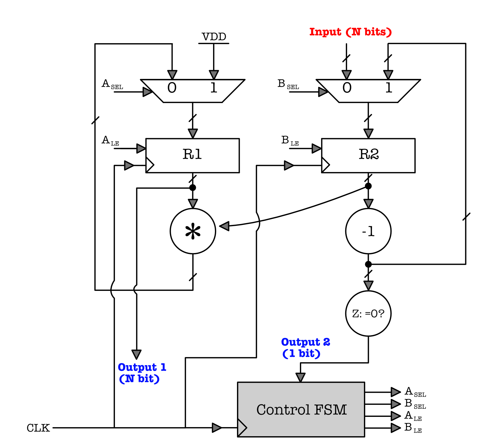
For example, let’s say we have Control FSM unit type $A$ that has the following functional specifications (its starting state is $S_0$):
\[\begin{matrix} S_i & S_{i+1} & A_{SEL} & A_{LE} & B_{SEL} & B_{LE}\\ \hline S_0 & S_1 & 1 & 1 & 0 & 1\\ S_1 & S_2 & 0 & 1 & 1 & 1\\ S_2 & S_3 & 0 & 1 & 0 & 0\\ S_3 & S_3 & 0 & 0 & 0 & 0\\ \hline \end{matrix}\]This specification allows Machine $M$ to be able to compute $\text{Input}\times(\text{Input}-1)$ at the $4^{th}$ clock cycle (counted from the moment stable input is fed – assuming this is the first cycle t=0). The answer will be ready at the
output1port at t=3 later after feeding in the input to the machine.
Take some time to analyse the datapath by running it with some small input value, e.g: Let $N=6$ and Input = $5$ =
000101(in 6 bits). So for example, at $t=0$ we know that Input $=5$ and $S_{t=0} = S_0$. Ask yourself:
- What is the value of “Output 1” and $S_{t=1}$ at $t=1$?
- Has “Output 1” contained the answer at $t=1$?
- What about at $t=2$?
- Confirm at which timestep $t$ will we have the correct value of $\text{Input}\times(\text{Input}-1) = 5\times 4 =20$ =
010100at “Output 1” port?
Now let’s say we have another control FSM unit $B$ that has the following functional specifications (Note: “$--$” means “does not matter”, and its starting state is also $S_0$):
\[\begin{matrix} Z & S_i & S_{i+1} & A_{SEL} & A_{LE} & B_{SEL} & B_{LE}\\ \hline -- & S_0 & S_1 & 1 & 1 & 0 & 1\\ 0 & S_1 & S_1 & 0 & 1 & 1 & 1\\ 1 & S_1 & S_2 & 0 & 1 & 1 & 1\\ -- & S_2 & S_2 & 0 & 0 & 0 & 0\\ \hline \end{matrix}\]This specification allows Machine $M$ to be able to compute $\text{Input}$ factorial and produce it at the “Output 1” port on after certain time steps. Similarly, take some time to analyse the datapath by running it with some small input value, e.g: Let $N=2$ and Input $=3$ =
11(in 2 bits), and find out how long it takes to produce the correct output: $3! = 3\times 2 =6$.
The programmability feature of machine $M$ allows us to reuse datapaths to solve new problems. However machine $M$ cannot be called a general purpose computer because:
- It has very limited storage: it can only read input of $N$ bits, whatever that is being fed in.
- It has a tiny repertoire of operations: $\text{Input}$ factorial and $\text{Input}\times(\text{Input}-1)$.
- It is unable to generate a new program and execute it. We need to replace the entire Control FSM unit for it to be able to be “reprogrammed”. In other words, theres no basic instruction set that can be used as building blocks to create a more complex programs to control it.
Now it is clear that what we need to do to create a general-purpose computer is to:
- Design a general purpose data path, which can be used to efficiently solve most problems, and
- Design a proper instruction set to allow for easier ways to control it.
The Von Neumann Model
Many architecture approaches to a general-purpose computing device have been explored (see others here), but the Von Neumann Model is one where most modern and practical computers are based on.
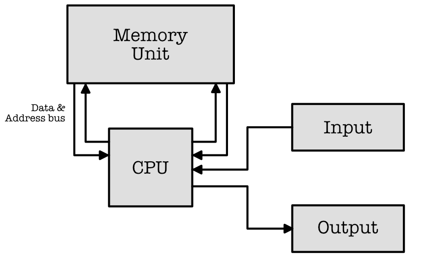
The generic anatomy of a Von Neumann architecture is shown above. The four main components of the model are:
- Central Processing Unit (CPU): the “brain” of the computing device, made up of several registers as internal storage, as well as combinational logic units for performing a specified set of operations on their contents.
- Memory Unit: external storage of data and programs that can be loaded onto the CPU and executed
- Input/Output: Devices for communicating with the outside world.
- Data/Address bus that connects all components of the machine together.
The Basic Anatomy of a Central Processing Unit
The CPU is a part of the computer that executes instructions. A series of these executable instructions is called a computer program. Before building a CPU, one usually design a figurative blueprint for how the CPU operates and how all the internal systems interact with each other. This blueprint is called the Instruction Set Architecture. There many different types of ISAs a CPU can be built on. Some of the common ISA families are x86 (found in desktops and laptops) and ARM (found in embedded and mobile devices).
A basic anatomy of the CPU is shown below, consisted of four major components: the Data Path, Internal Storage called REGFILE, consisted of many Registers (e.g: D Flip-Flops), the Arithmetic Logic Unit (ALU), and a Control Unit (FSM).
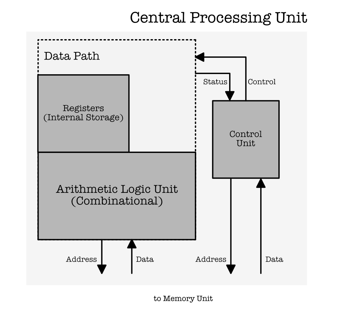
The CPU is essentially “brain” of the computing device, and it is be able to:
- Load a series of instructions (from the Memory Unit),
- Produce the corresponding control signals, hence effectively “executing” that loaded instruction using the combinational logic unit (the ALU).
- And store them in its (limited capacity) internal storage
- It is also capable of storing the computed output back to the Memory Unit.
The Data Path is an overarching infrastructure to control what input goes to each component, and where the output of each component in the CPU goes to.
The Control Unit is made of a program counter (PC) and a control unit (CU). The job of a PC is to read an instruction (at a time) from the Memory Unit, so that the CPU can execute it. The CU gives us the control signals based on that current instruction read. These signals control the datapath and enable us to route data to the appropriate components stated in the instruction.
The Arithmetic Logic Unit performs the “work” – computing basic functions such as addition, comparison, boolean, shifting, and multiplication.
A great explanation quoted from this source: “You may imagine a CPU as a train car.”
“The engine is what moves the train, but the conductor is pulling the levers behind the scenes and controlling the different aspects of the engine.
A CPU is the same way. The datapath is like the engine and as the name suggests, is the path where the data flows as it is processed. The datapath receives the inputs, processes them, and sends them out to the right place when they are done.
The control unit tells the datapath how to operate like the conductor of the train. Depending on the instruction, the datapath will route signals to different components, turn on and off different parts of the datapath, and monitor the state of the CPU.”
The Memory Unit
The CPU is able to read and write bits of data to and from a memory unit connected to it – an expandable storage device (we know it as RAM in practice).
As the name suggests, this device does NOT execute anything, it simply retains (store) information.
The “data” that is stored in this expandable resource pool is not just simply inputs, i.e: images, videos, documents, etc, but also instructions that make up a program. This is where your instruction resides when it is about to be executed by the CPU.
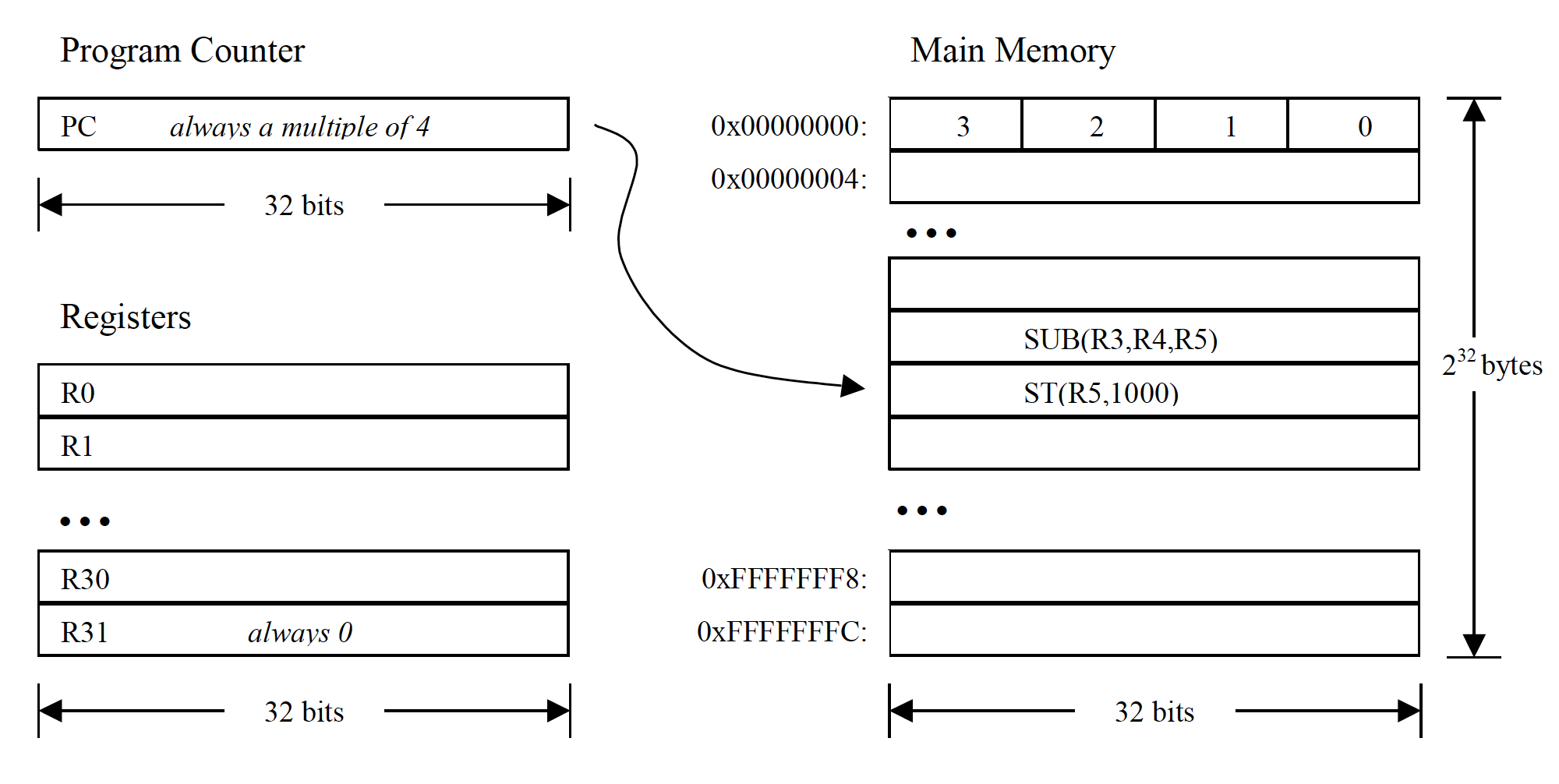
Since the memory unit can store a huge amount of data (in Gigabytes), the CPU must be able to read just a particular $N$ bits of relevant data from the memory unit. It is able to do this by giving an address as an input to the memory unit. The memory unit receives this address and output the data stored at the given address. To write onto the memory unit, the CPU must provide two inputs: the address where this $N$ bits of data should be stored, and the data itself.
We will learn more about the anatomy of the memory unit, but for now we can think of it as a device that can store a huge amount of data, separated into addressable segments that can hold $N$ bit of data each, as shown in the figure below. It generally receives three kinds of input, 1-bit WE signal (write enable), address, and data input (bit size varies, depending on how much data can the memory holds).
Think of a memory unit as similar to a storage facility that has a large amount of storage units. Each unit has the same volume, and it can store a bunch of objects in it. People usually can rent these units to place their belongings.
If we rent such unit, we are typically given an address – some kind of index to identify the unit that is ours. The $N$-bit data is the “object” that we put in a storage unit (addressable segment), and the memory address is the identifier of the storage unit location where the data is held.
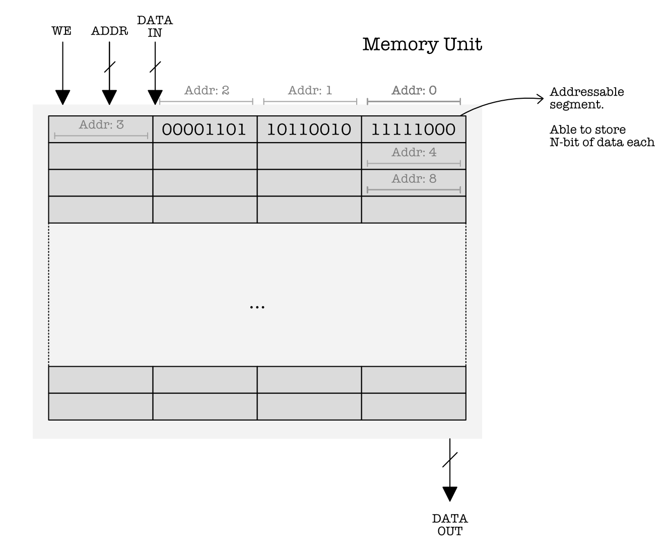
Important : below are the list of conventions that explain why we illustrate the memory unit as above.
-
We illustrate the memory unit to have four segments per row. This is only for illustration purposes, so that we can read them on paper more easily. In practice, it doesn’t matter how you physically arrange the segments.
-
Each segment can contain exactly 8 bits of data (1 byte) – this is done by convention.
-
Each segment of 8 bits (1 byte) is addressable. Therefore we say that by convention, data in the memory unit is byte addressable.
-
In each row (series of 4 segments), lower addresses are written on the right, and higher addresses on the left (hence address 0 is given for the most upper right segment and so on).
-
Each row contains $4\times8$ bits in total $=32$ bits.
- A memory unit typically receives $N$ bits of data input. Similarly, it typically outputs $N$ bits of data at a time, where $N=32$ or $N=64$. In this course, we will learn a 32-bit toy architecture (called the $\beta$) and therefore we will always $N=32$.
Therefore we will illustrate the memory unit to always have four 8-bit segments per row in this course – because it receives input or produce output in chunks of 32-bit data at time.
Modern computers in 2020 typically adopt the $64$ bit architecture (so we have 64-bit words for these architecture) .
- The number of bits that can be received in ADDR input port is either fixed (also 32 bits for this course) or depends on how many bits are needed to address all the segments in the memory unit.
For example, if we have a memory unit of size $128$ KB = $128 \times 1024 = 131072$ bytes, we need at least $\log_2(131072) = 17$ address bits. It is alright to receive more address bits.
What is the maximum memory unit size that we can have with $32$ address bits?
- In the figure above, each row contains $4\times8$ bits in total $=32$ bits. We call a block of
32bits as a word. Since the memory unit is byte addressable, a 32-bit word has four addresses. By convention, we select the smallest of the four addresses to be the overall address of the word.- So for example in the figure above, the first word (in the first row), has address
0x0000. - The subsequent word in the second row has address
0x0004, and so on. - Each subsequent word has their addresses increased by 4.
The definition of a word actually may depend on the ISA. The computer model that we learn for this course is a 32-bit architecture, therefore we define 1
WORDto be 32 bits.
- So for example in the figure above, the first word (in the first row), has address
Programmability of a Von Neumann Machine
We can clearly see how electronic devices that are designed based on this model is programmable (i.e: a close physical manifestation of a Universal Turing Machine).
The Memory Unit represents the “tape” of the Universal Turing Machine, while the CPU is the “arrow” that performs the logic computation and perform read/write to the memory. Both “input” and “program” (instructions) can be stored in the memory unit.
In the real world however, we can never have an infinitely long tape.
The CPU is a complex sequential logic circuit – a datapath whose job is to fetch and execute instructions loaded from the memory, one instruction at a time per clock cycle.
The Control Unit provides different control signals depending on the current instruction read. This allows us to reuse the same data paths for computing a set of different functions – or in other words: provide programmability. Programmable data paths give some algorithmic flexibility, achievable by just changing the control structure.
What are these “instructions”? How do we design an instruction set that makes for a general purpose programmable device? Designing an instruction set is a mix of engineering and art: we need to design an instruction set that is compact, uniform, versatile, fast, and so on.
Trial by simulation is our best technique for making choices.
In this course, we will learn the $\beta$ instruction set – an instruction set architecture (ISA), a CPU blueprint that defines an abstract model of a general-purpose computer. It specifies many crucial information that describes how a CPU should work, such as what instructions the CPU can process, how it interacts with the memory unit, the basic CPU components, instruction formats, and many more.
Its implementation: the $\beta$ CPU, is a 32-bit Von Neumann-based toy CPU created by MIT as a teaching tool to introduce students to programmable datapaths and instruction sets, among all others. We can write any algorithm using a mixture of $\beta$ instructions. The CPU can emulate any machine behaviour that we want by executing it.
Modern ISAs (e.g: ARM, x86) and its corresponding CPU architecture is certainly much more complex than the $\beta$, however the $\beta$ is more than sufficient for us to understand and appreciate the basic concepts of programmable datapath and instruction sets. Some notable ISA in the past are 6502, AVR, and 32-bit x86.
The Beta Instruction Set Architecture
Recall that in order for a machine to be programmable (used for general purpose), we need to design a set of well-defined operations (supported functions that can be computed), that the machine should support. These operations can be used to form a larger – more complex program that if executed, allows the machine to emulate the behavior of another program.
Beside defining the machine’s operation types, the ISA should also define the supported data types, the registers (How many internal registers are there? How to address them? etc), and various other fundamental features such as addressing mode, input and output, and many more.
Let’s dive in to the $\beta$ ISA right away.
$\beta$ ISA Format
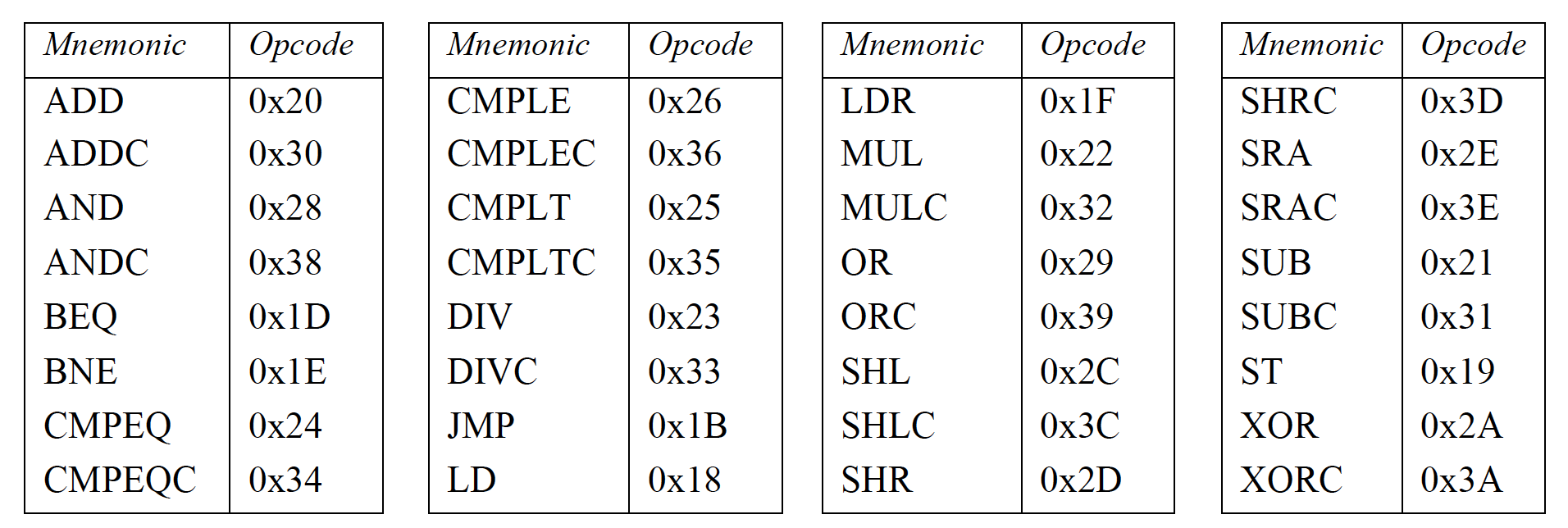
Each instruction that the $\beta$ supports is written in a specific encoding. There are in total of 32 disctinct operations/instructions that the $\beta$ should be able to execute, each having its own operation encoding (OPCODE).
The complete documentation on each instruction in detail can be found here.
All instructions have the same characteristics:
- Each instruction is encoded into 32-bits of information.
- Only one instruction is executed in each clock cycle. Each instruction is considered atomic and is presumed to complete before the next instruction is executed.
$\beta$ Machine Model
The $\beta$ is a general-purpose 32-bit architecture. All registers are 32 bits wide. There are 33 registers in total (in the entire CPU):
- The PC register: contain the address of the instruction that’s supposed to be executed by the CPU.
- When loaded with an address, it can point to any location in the byte-addressed memory.
- The memory unit returns the instruction (32-bit data) stored at this address for the CPU to decode and execute.
- The REGFILE registers (internal storage in CPU): contains 32 registers in total (and each register is 32 bits wide), addressable with 5 bits to identify
R0toR31respectively.- All registers except
R31can be read or written with new values. - For
R31: when read, it is always 0; when written, the new value is discarded. - Notation: In register transfer language, the content of register with address
Ais often denoted as :Reg[A]. The symbolRxrefers to the address of a particular registerxin the REGFILE. The symbolReg[Rx]refers to the content of that register.
- All registers except
Its machine model is summarised in the figure below:
Note that :
-
The Memory Unit (main memory) can also be referenced through load and store instructions that perform no other computation. The target memory address should be loaded in any registers in the REGFILE.
-
Conditional branch instructions (BEQ and BNE) are separated from comparison instructions (CMPLE, CMPLT, CMPEQ).
Branch instructions test the value of a register that can be the result of a previous compare instruction.
$\beta$ Instruction Encoding
There are only two types of instruction encoding: Without Literal (Type 1) and With Literal (Type 2). All integer manipulation is between registers, with up to two source operands (one may be a sign-extended 16-bit literal), and one destination register.
- Instructions without literals (Type 1) include arithmetic and logical operations between two registers whose result is placed in a third register.
- Instructions with literals (Type 2) include all other operations and instruction literals is represented in two’s complement.
The figure below shows the two types of $\beta$ instruction encoding:
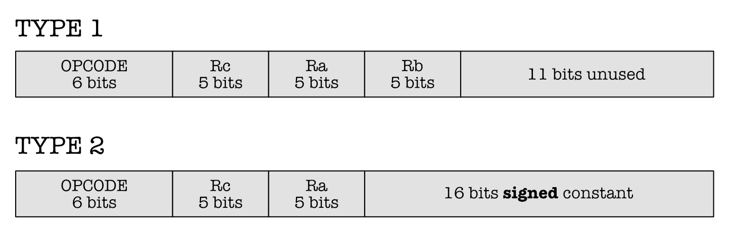
The 32-bit instruction I is segmented to various sections:
- The
OPCODE =I[31:26]is 6 bits long. TheOPCODEsignifies different types of operation. They are summarised in the table below:
- For Type 1 instruction (without literal), we have these three segments:
Rc = I[25:21],Ra = I[20:16], andRb = I[15:11], each 5 bits in length, to signify the target address of the registers in the REGFILE. The last 11 bits are unused.Rcis the destination register to write output to.Ra, andRbcontain the source data
- For Type 2 instruction (with literal), we have these three segments:
Rc = I[25:21],Ra = I[20:16], andc = I[15:0].Rcis the destination register to write output to.Racontains the source data.cis a 16-bit signed constant or literal.
The reason for this Type 2 instruction is that some operations require a constant instead. For examplem we want to add the content of register
Rawith a constantc$= 4$ instead. Then we can encodec=0000 0000 0000 0100as the last 16 bits of the instruction.
Example 1:
- Suppose we have following 32-bit instruction: $I=$
110000 00011 00001 1111111111111101 - Refer to the $\beta$ documentation, and we can find that first 6 bits corresponds to the
OPCODE: ADDC(Type 2) - Segment the instructions:
Rc = I[25:21] = 3,Ra = I[20:16] = 1, andc = -3. - Refer to the $\beta$ documentation to find out what ADDC does:
- To add the content of Register
R1withc = -3 - And store it in Register
R3 - Increase the content of PC by 4
- In register sign language:
PC$\leftarrow$PC+4Reg[Rc]$\leftarrow$Reg[Ra]+SEXT[c]Since
cis 16 bits, it has to be sign-extended (SEXT) to be 32 bits before added with the content ofRa.Regrefers to the REGFILE andReg[Rx]means the content of register addressed asRxin the REGFILE. We end up withc=0xFFFFFFFD.
- To add the content of Register
Example 2:
- Now suppose we have the following 32-bit instruction: $I=$
011001 01001 00011 0000000000001000 - Refer to the $\beta$ documentation, and we can find that first 6 bits corresponds to the
OPCODE: ST(Type 2) - Segment the instructions:
Rc = I[25:21] = 9,Ra = I[20:16] = 3, andc = 8. - Refer to the $\beta$ documentation to find out what ST does:
- To store the content of
Rcto the memory unit - In address: content of
Ra+c - In register sign language:
-
PC$\leftarrow$PC+4-EA$\leftarrow$Reg[Ra]+SEXT[c]-Mem[EA]$\leftarrow$Reg[Rc]>EAmeans effective address.Mem[EA]refers to the content of the Memory Unit at address EA. Againcis sign extended to form 32 bits:0x00000008.
- To store the content of
It is imperative that you read the beta documentation up until page 12, to understand all 32 basic instructions of the $\beta$ machine individually before proceeding to the next chapter. In the next few weeks, we will take this knowledge to the next level as you learn how to hand assemble C-language into this low-level machine language.
High Level language, Assembly Language, and Machine Language
We usually code in higher level language such as Python, Ruby, C/C++, Java, Javascript, C# and so on. However, our machines do not understand these languages directly. The human-friendly, intuitive high-level programming syntaxes are ultimately just a bunch of ones and zeros stored inside the machine.
Our high level languages, are first translated into assembly language, before further converted into machine language in its binary form.
For example, we can write the following in C:
int x = 3;
x = x + 10;
The compiler (GCC, for example) compiles the code above and translate it into the appropriate assembly language. Suppose we are running it on a $\beta$ machine and that the compiler supports it, the code above will be translated into $\beta$ assembly as an intermediate step:
LDR(x, R0)
ADDC(R0, 10, R0)
ST(R0, x) | Note this is a "macro" for ST(R0, x, R31). You'll learn "macro" in later parts.
x : LONG(3)
Finally, it will be converted into $\beta$ machine language, 32-bit for each line of assembly code. We may know this as an “ executable”, that is a piece of information that is directly “understandable” by the machine without the help of an intemediary translator anymore like a compiler/interpreter, or an assembler:
011111 00000 11111 0000 0000 0000 0010
110000 00000 00000 0000 0000 0000 1010
011001 00000 11111 0000 0000 0000 0000
0000 0000 0000 0000 0000 0000 0000 0011
The difference between each type of language is obvious.
- Firstly, it is nearly impossible to directly code in binary format, and much more convenient to code using the higher language.
- Secondly, converting from high level language to assembly language is a little bit more complex (and not unique, meaning that there are many ways to translate the high level language to the assembly language that still results in the same output) than to convert from assembly to the machine language.
Don’t worry yet as of now. What we need to know (and get familiar with) is simply how to do this task: given a 32-bit machine language, write the corresponding assembly instruction and explain how it works (and vice versa).
Preview: The $\beta$ CPU
The $\beta$ CPU falls under the family of RISC (reduced instruction set computing) processor. This type of computer processor possesses a small but highly optimised set of instructions, and are currently used for smartphones and tablet computers, among other devices.
The full anatomy of the (general-purpose) $\beta$ datapath is shown in the Figure below. Remember that this is an implementation of the $\beta$ instruction set architecture (i.e: its abstraction). This circuitry is therefore able to execute any $\beta$ instruction as intended within a clock cycle.
The details of the $\beta$ datapath will be explained in the next chapter, so that you have a complete understanding on how the datapath allows the working of each of the 32 instruction sets.
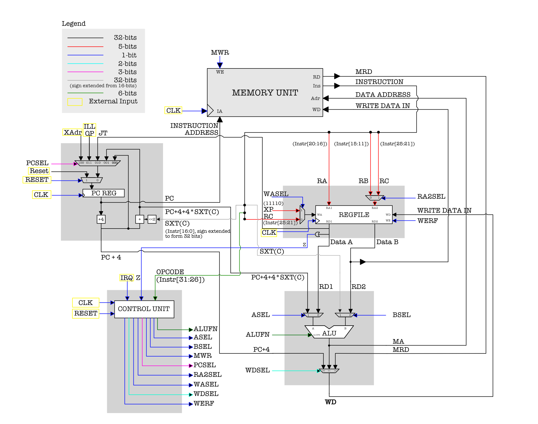
As of right now, we just need to understand the big idea of the $\beta$ ISA , and how the $\beta$ CPU realises it:
- The PC (program counter) is a part of the CPU that in theory, fetch one instruction (set to be 32-bit in length) from the Memory Unit per clock cycle.
- The
OPCODEpart of the instruction is processed by the Control Logic unit, and appropriate control signals are produced. - The combination of these control signals reprogram the datapath so that we can reuse it to execute different types of instruction.
- The other parts of the instruction:
Rb,Ra,Rcorc, tells us which registers in the REGFILE to use for this instruction. - Step 1-4 are repeated for each clock cycle, and each instruction is atomic.
The $\beta$ CPU hardware is therefore designed so that it can implement the $\beta$ ISA, and therefore we can give an actual physical form (of a machine) that is programmable and able to execute each defined $\beta$ instruction correctly as intended.
Summary
In the beginning of this chapter we were given the programmable Machine $M$, that is capable of computing the simple factorial function. We then proceeded by arguing that Machine $M$ is not enough to be used for a general purpose machine, that is to be used as an implementation of a Universal Turing Machine.
What we need to do to create a general-purpose computer is to:
- Design a general purpose data path (architecture), which can be used to efficiently solve most problems, and
- Design a proper instruction set to allow for easier ways to control it.
The $\beta$ ISA and its implementation, the $\beta$ CPU fulfils both requirement. If used to execute proper instruction, it should be able to emulate what Machine $M$ is able to do.
So how do we write the code to do factorial in a way that $\beta$ CPU can execute?
Suppose we have the simple factorial program written in $C$:
Unlike in Python, in C we cannot write standalone instructions without declaring a function. We will learn function linkage procedure in Week 9. For now to simplify, assume that instructions below are part of some pre-defined function in some .c script.
int n = 9; // or 10, or 11, any constant
int ans;

int r1 = 1;
int r2 = n;
while (r2 != 0){
	r1 = r1 * r2;
	r2 = r2 - 1;
}
ans = r1;
This can be (hand) assembled into $\beta$ assembly language:
.include beta.uasm

ADDC(R31, 1, R1)        | R1 = 1
LD(n, R2)               | R2 = n

loop:
BEQ(R2, done, R31)      | while (R2 != 0)
MUL(R1, R2, R1)	        | R1 = R1 * R2
SUBC(R2, 1, R2)	        | R2 = R2 -1
BEQ(R31, loop, R31)     | Always branches!

done:
ST(R1, ans, R31)        | ans = R1
HALT()

n: LONG(9)
ans: LONG(0)
Of course then the final step is to convert this into machine language and load it to the Memory Unit, and allow the PC of the $\beta$ machine to execute the first line of instruction (ADDC) .
You can actually do this! Open
bsim.jar, paste the assembly code above and run it.
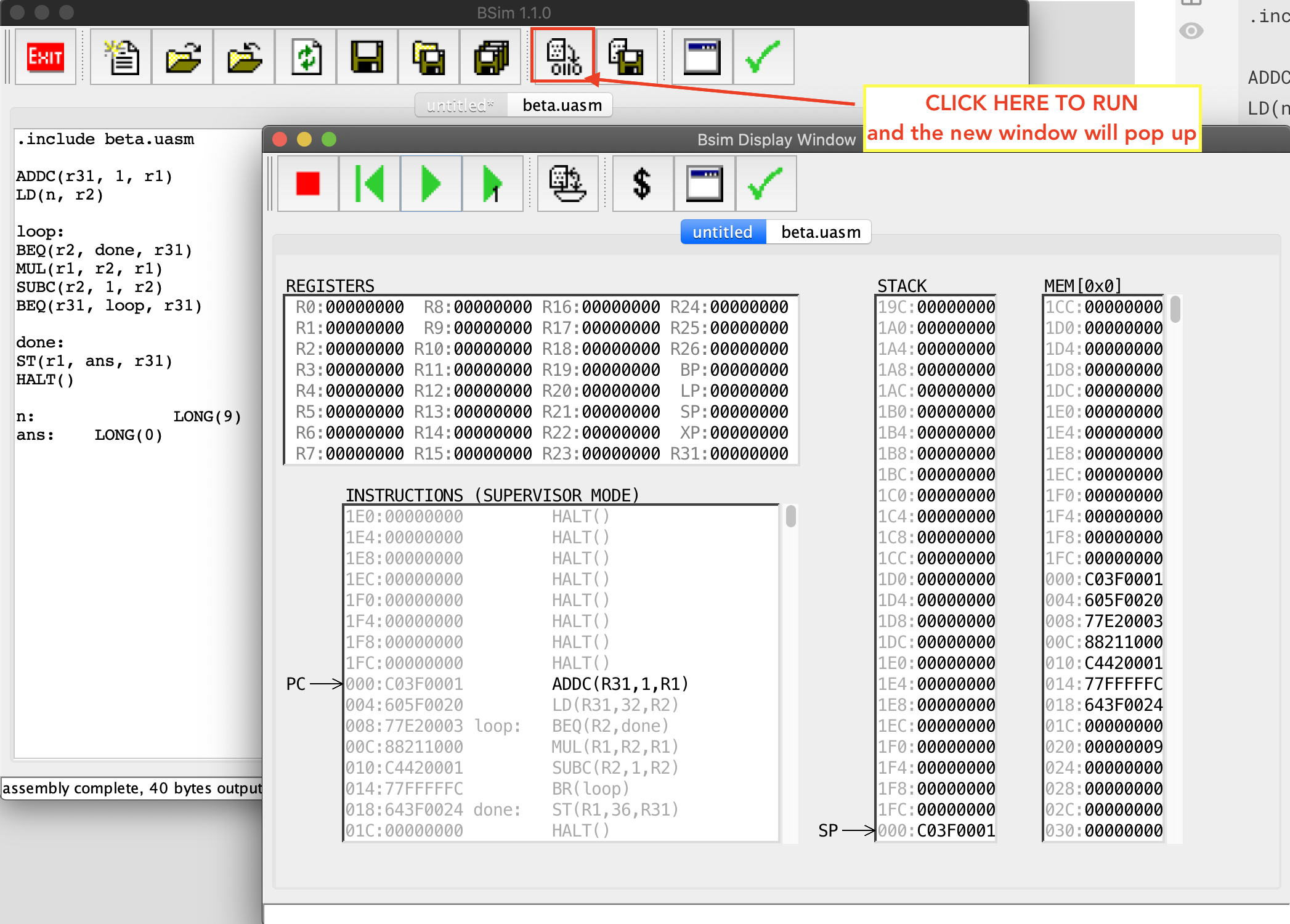
When the machine halts, we should have the answered stored somewhere in the memory unit, thus effectively enabling $\beta$ machine to emulate the ability of Machine $M$ without changing its datapath.
We will learn more about how to hand assemble and manually execute the code soon. Right now, this is here to give you a preview of what is to come in the next few weeks.