 Computation Structures
50.002 Computation Structures
Information Systems Technology and Design
Singapore University of Technology and Design
Digital Abstraction
Overview
One of the cheapest ways to encode information is in terms of 0s and 1s, using voltages. This method of determining discrete values out of voltages (which value is originally made up of real number, and therefore continuous and infinite) is called the digital abstraction.
What are the benefits of the digital abstraction?
- The digital abstraction is where one interprets voltage values as binary values, thus allowing us to encode information using voltages.
- Using voltages to encode bits of 0’s and 1’s provides a cheap and stable way for us to exchange information through digital devices.
- We can also manipulate or change information encoded using voltages very easily.
The voltages that represent digital bits are generated by semiconductor devices (MOSFET) – something that we will learn in the next chapter. The benefit of using semiconductors the ease of generation, and that they require zero power in steady-state. The drawbacks however, is that the voltages generated by these semiconductors are easily affected by external disturbances, and hence they may be unstable.
To preserve the integrity of information encoded in digital devices made of semiconductor materials, we need to set some contracts between these interconnected digital devices. In this notes, we are going to learn how we can use voltages to encode information in a stable way that follows a particular contract called the static discipline to guarantee the behavior of each processing block in the system.
A Digital Processing Element: Combinational Device and Combinational Digital System
A digital device is any device that uses voltages to encode information in terms of “low voltage” (bit 0) and “high voltage” (bit 1). Its output is a pure function of the present input only (there’s no memory of past inputs), and it has the following criteria.
A combinational device is a specific type of digital device that has the following criteria:
- One or more digital inputs
- One or more digital outputs
- A functional specification that details the value of each output for each possible combination of inputs (can be illustrated in terms of truth table / boolean expression)
Its circuit performs an operation assigned logically by a boolean expression or truth table.
- A timing specification consisting of an upper bound required
propagation time for the device to compute the specified output
values given a set of valid and stable input value(s)
Later on you will learn another type of digital logic devices called the sequential logic device, whose output depends not only on the present input but also on the history of the inputs, hence having a memory.
A set of interconnected circuit elements is combinational and can be labeled as a combinational digital system if and only if:
- Each circuit element is also combinational with no directed cycles (no feedback loop), and
- That very device’s input is connected to exactly one output of another device or to some vast supply of ‘0’s and ‘1’s.
Voltage to encode information
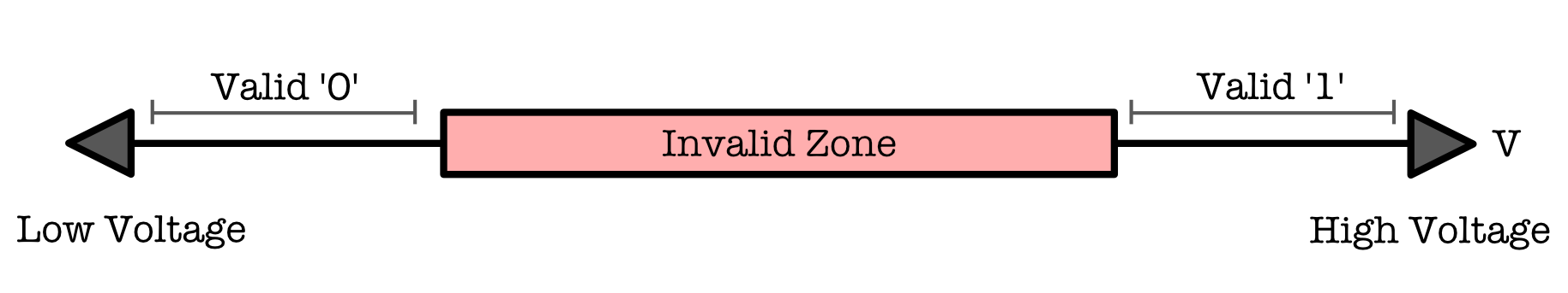
The most naive way to use voltage to encode information is to use ‘low’ voltage to encode valid ‘0’ and ‘high’ voltage to encode valid ‘1’, and define the low and high threshold for each valid ‘0’ and ‘1’.
Anything that is between the low and high threshold value is called the invalid zone, as shown in the figure below:
The static discipline is one of the contracts bound for all logical elements making up a digital system. The static discipline is stated as follows:
A digital system must be able to produce a valid output (for the next device connected at its output terminal) according to its specification if it is given a valid input.
This contract guarantees the behavior for each processing block in a system, so that a set of such interconnected devices may work properly (are able to pass and compute valid information at the end of the chain of connections). This is necessary so that the system has a predictable behavior.
However this doesn’t mean that the opposite is true. a device that receives invalid input does not always have to produce invalid output. We don’t care much and cannot define or guarantee the behaviour of the combinational device if it receives invalid input – it may or may not produce a valid output.
Therefore, one can say that a combinational logic device always obeys the static discipline.
Voltage Specifications and Noise Margin
Consider two digital devices connected in series as shown in the figure below. These devices are called a buffer, meaning that they pass the same bit over (if it receives a low voltage, it will produce a low voltage and vice versa). If we were to naively decide that any voltage below $V_{low}$=0.5V as digital bit 0, and any voltage above $V_{high}$=2.5V as digital bit 1, then our device may violate the static discipline.
Why is this so?
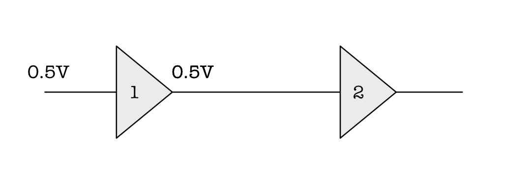
This explanation can be made clear with the following example. Suppose we supply 0.5V and Device 1 is able to produce also 0.5V, which means digital bit .
- However, the problem is that a wire, that connects two or more combinational devices together is susceptible to noise.
- The voltage value that is received at Device 2 may be slightly higher than 0.5V, for example: 0.55V instead, and therefore according to our specification, it is no longer a valid bit ‘0’.
Note that a noise can knock the voltage down as well, this is just an example that’s detrimental to the function of the devices in this example.
Device 1 in the figure above violates static discipline because given a valid input, it *may be unable to produce a valid output (to reach the next device 2)*, because the 0.5V produced at the output of Device 1 may meet some disturbances that caused it to be slightly off, e.g: 0.55V.
Hence, we need to account for the presence of some light noise.
Instead of naively setting some voltage $V_{high}$ and $V_{low}$ as we did above, we need to set a range of Voltages as valid bit 1 and 0 respectively, and ensuring that we
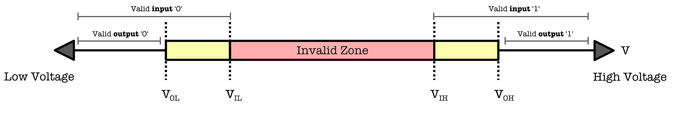
Hence, we need to have something called the noise margin – the yellow region illustrated in the Figure below. The noise margin is formed by setting four Voltage specifications: $V_{ol}$, $V_{oh}$, $V_{il}$, $V_{ih}$, where $V_{ol}$< $V_{il}$< $V_{ih}$ < $V_{oh}$ which defines what range of voltage values signifies a valid digital bit and a valid digital bit 0 for any combinational logic component in the system:
The noise margin adds as a precaution against external disturbances (noise).
Below are the explanations necessary to understand the fFigure 3 above:
-
$V_{ol}$ (voltage output low) and $V_{oh}$ (voltage output high) is the voltage that your system outputs, depending on whether your system is outputting bit
0or ‘1’. The output of this system is going to be received by another system after traversing through some wire. -
$V_{il}$ (voltage input low) or $V_{ih}$ (voltage input high) is the voltage that your system receives as input from another system.
- The absolute difference between $V_{ol}$ and $V_{il}$ is called the low bit noise margin, and the absolute difference between $V_{oh}$ and $V_{ih}$ is called the high bit noise margin.
Noise margin is formally defined as the maximum voltage amplitude of extraneous (erronous) signal that can be added to the noise-free input level without causing a drastic change in the output voltage and that it is still within the valid logic level.
-
The noise immunity (like an “overall” or “effective” noise margin) is the minimum between the high bit noise margin and the low bit noise margin.
-
$V_{ol}$ is less than $V_{il}$, because we would want to have some buffer against noise. A device always outputs a lower voltage value to signify digital bit
0‘0’ and accepts a slightly higher low-voltage value as digital bit0‘0’. The same logic applies for the higher region as well, as $V_{oh}$ is greater than $V_{ih}$ - In our previous case in Figure earlier, if $V_{ol}$ is set to be
0.5V, and $V_{il}$ is set to be0.6V, then Device 2 will be able to tolerate up to0.1Vof noise (if any). Therefore,0.55Vin our example above is still ‘seen’ as a valid bit0when it arrives at the input terminal of Device 2, thus making Device 1 obeys the static discipline.
Once set and chosen, these four voltage specifications: $V_{ol}$, $V_{oh}$, $V_{il}$, and $V_{ih}$ are to be obeyed by every digital device in an entire combinational logic circuit.
Voltage Transfer Characteristic Function (VTC)
The VTC is a plot between the input voltage ($V_{in}$) to a digital system/device vs the output voltage ($V_{out}$) of this digital system.
VTC does not tell us how fast the device is. It just captures the static behavior of the device and tells us what kind of device it is.
The image below shows the VTC of a buffer: a low $V_{in}$ gives a low $V_{out}$ and vice versa.
What will the VTC of an inverter look like?
The purpose of plotting a VTC (typically obtained from device measurements, i.e: we supply input voltages at intervals and measure the output) helps us to determine whether or not a digital device can be used as a combinational logic device.
In other words, to find out if we can find a set of four voltage specifications: $V_{ol}$, $V_{oh}$, $V_{il}$, and $V_{ih}$ for the device so that the device obeys the static discipline.
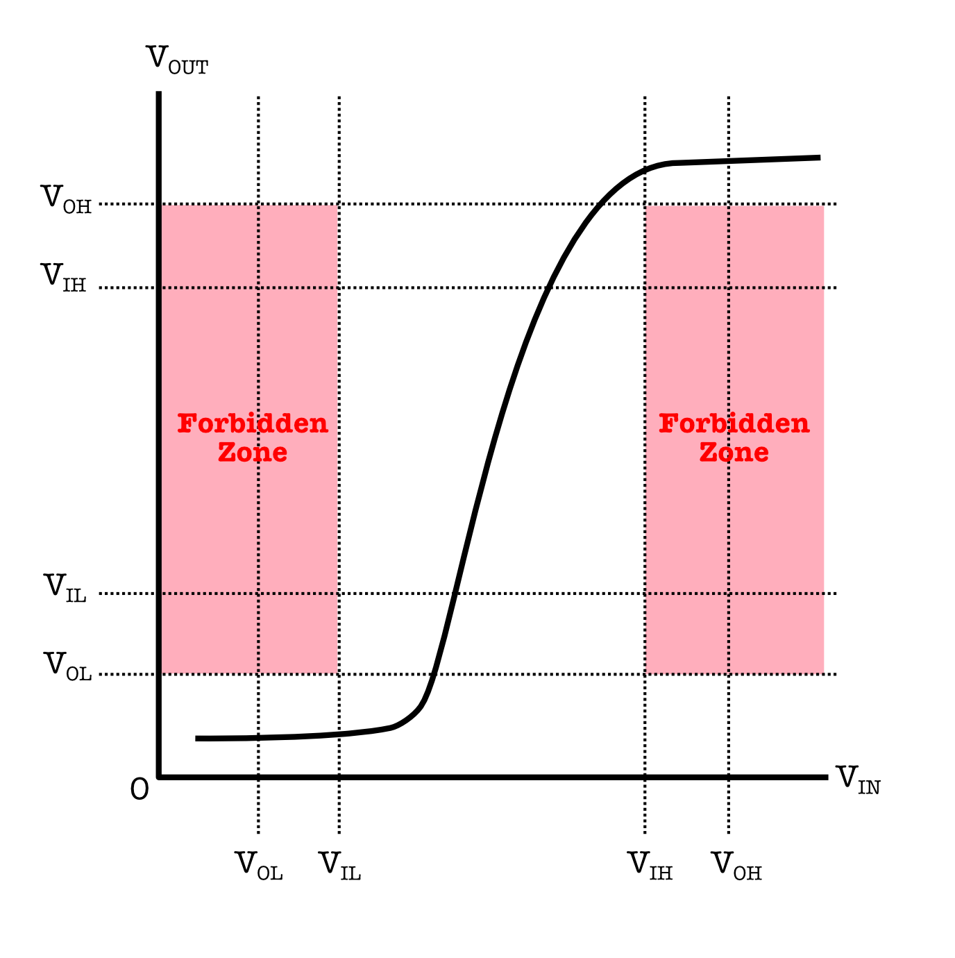
Explanation of the VTC figure above:
- The red zone is called the forbidden zone. It is formed by the four voltage specifications: $V_{ol}$, $V_{oh}$, $V_{il}$, and $V_{ih}$ that we set for the entire system.
- The name ‘forbidden zone’ comes e the fact that any value within this zone means that the device receives valid input but is unable to produce a valid output hence violating the static discipline and cannot be used as a combinational logic device.
You can quickly tell if a digital device can be potentially be used as a combinational logic device iff: you can find a set of these four voltage specifications: $V_{ol}$, $V_{oh}$, $V_{il}$, and $V_{ih}$ whereby its VTC curve does not cross the forbidden zone and that $V_{ol}$< $V_{il}$ < $V_{ih}$ < $V_{oh}$.
-
We typically begin by guessing each value of $V_{ol}$, $V_{oh}$, $V_{il}$, and $V_{ih}$ and check if the curve crosses the forbidden zone (check if static discpline obeyed) formed by these four values.
- If static discipline is violated, we either adjust our guess or find another device.
- Also, we want to choose $V_{ol}$, $V_{oh}$, $V_{il}$, and $V_{ih}$ that maximises noise immunity. -
If you can satisfy the condition highlighted above, then it means that the device is a combinational logic device. It’s VTC curve has to possesses both characteristics below:
-
There exist some region in the VTC whereby its absolute
\[\begin{aligned} \text{Gain}(V_{in}) = \frac{d V_{out}}{d V_{in}} \end{aligned}\]Gainis $>1$ .Gainis actually a function of $V_{in}$ and is formally defined as:In laymen terms you can approximate
\[\text{Gain} \approx \frac{V_{out_l}-V_{out_k}}{V_{in_j}-V_{in_i}}\]Gainduring some transition $V_{in_i}$ to $V_{in_j}$ that results in some $V_{out_k}$ to $V_{out_l}$ respectively by the simply computing the slope between these two points on the VTC:If you have found four voltage specifications $V_{ol}$, $V_{oh}$, $V_{il}$, and $V_{ih}$ for which the device still obeys the static discipline, you can approximate device’s maximum
\[\max\text{Gain}\approx \frac{V_{oh} - V_{ol}}{ V_{ih} - V_{il}}\]Gainby computing: -
If absolute
Gain$>1$, then there is a finite, positive noise margin. If absoluteGain$=1$, then there’s zero noise margin. It is impossible to have absoluteGain$<1$ and still have the four Voltage specifications $V_{ol}$ < $V_{il}$ < $V_{ih}$ < $V_{oh}$.You might want to ponder a little and convince yourself why the statement above is true.
Also, having absolute
Gain > 1maintains the signal passed through the system as signal loss is inevitable through the system. -
The device has a Non-linear
Gain, meaning thatGainis a function ofVinand therefore the gradient along the entire curve varies.- The VTC curve for a combinational logic device should not be entirely made of a single, constant gradient like the shape of a plot from a basic line equation, but rather more towards an “S” (or mirrored S) shape.
In other words, if both characteristics above aren’t satisfied in the VTC curve, then it is not the VTC of a combinational logic device.
Summary
In this chapter, we have learned about the digital abstraction, that is how can we set some contracts (via setting the four voltage specifications) such that we can establish digital values out of real-valued voltages.
In the next chapter, we will learn about the MOSFET (transistor), that is one of the smallest component (building block) that makes up a digital device, and how we can use them to form a proper combinational logic elements we call gates. These gates can be used to form an even larger combinational circuits such as the adder, shifter, etc, and an even larger one such as the Arithmetic Logic Unit (you will build them in Lab 2 and 3).
Each larger device will provide greater level of abstraction.
Therefore, it is imperative that each combinational logic device / component, no matter how small, must conform to the static discipline and the established four voltage specifications (that must be chosen such that it fits with their VTC) so that the larger system can work as intended.