50.002 Computation Structures
Information Systems Technology and Design
Singapore University of Technology and Design
Natalie Agus (Fall 2020)
Getting Started with FPGA: Part 2
This document introduces the steps on how we can create basic sequential logic modules, that is any module that utilises dff (D flip-flops).
You are recommended to read this document only after you have understood Week 3 materials, namely the synchronous logic and FSM.
The Alchitry Au board comes with 100MHz on-board clock. When used properly, connections defined in the always block of sequential logic modules is set by default to receive new set of values at every positive clock edge. It is imperative for dynamic discipline to be satisfied within a clock period. Designs that fail to pass timing but are used anyway will result in unpredictable output.
Sequential Logic Module
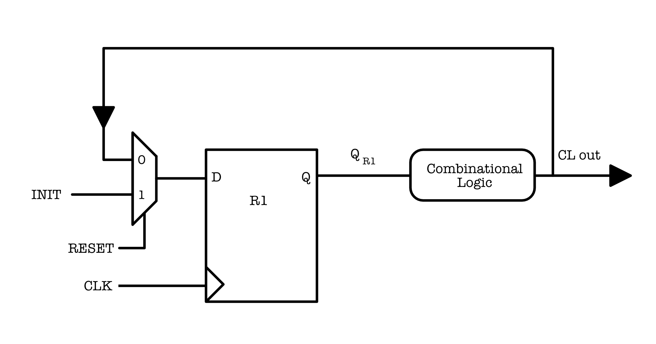
Above is a sample schematic of a simple sequential logic module. Assuming the D Flip-Flop R1 is triggered at each positive clock edge, then:
-
The combinational logic unit applies some function $f$ to its input
QR1. - At the first cycle, the value loaded to
R1isINIT, and hence at the signal atCL out= $f($INIT$)$ - At the second cycle, we apply $f$ again, resulting in
CL out= $f(f($INIT$))$, and so on. - We need to ensure that dynamic discipline is obeyed, meaning that $t1$ and $t2$ timing constraints are satisfied.
- Typically this isn’t much of an issue, unless you perform intensive computations in the combinational logic unit such that its
tpdgets too large and violates the $t2$ constraint. - Alchitry Lab will warn you if timing contraints are violated, which means you need to break down the combinational logic unit into smaller parts and adding more DFFs in between.
- Typically this isn’t much of an issue, unless you perform intensive computations in the combinational logic unit such that its
To make things simple, let’s use the 8-bit ripple-carry adder unit that we made in Part 1, to increment the value of INIT by the constant 2 at each clock cycle:
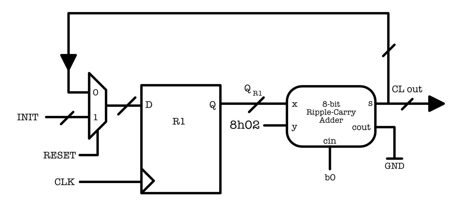
- The output
coutis grounded because we don’t need it. - The system has 8-bit
CL outas output. There’s no external input to the system. - When the system starts, it will add
2toINITvalue at each clock cycle. - If we connect each bit of
CLoutto an LED, then the output sequence we should observe (changing at each CLK cycle) is:2, 4, 6, 8, ...(in binary, of course).
Declaring and Using D Flip-Flop
We already have the 8-bit ripple-carry adder module ready, but not the D Flip-Flop. Fortunately, Lucid has a built in D Flip-Flop + the small reset mux built into it that you can use by declaring each unit with the keyword dff before the always block.
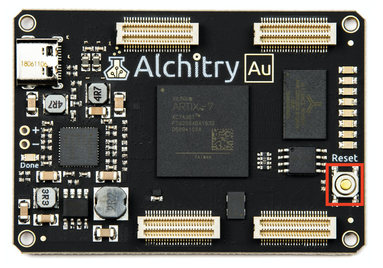
Create a new module and name it seq_plus_two.luc. This time round, we accept input clk and rst signal as per the default .luc script. These two signals are fed by the hardware, where clk is typically the onboard clock, and rst signal is 1 when the reset button on Alchitry Au (not Alchitry Io!) is pressed.
To use a dff properly, you need to define:
- The
clksignal, - The
rstsignal (optional), and - The
INITvalue (optional) .
All of the above must be done BEFORE the always block to take desired effect.
The syntax to define the so-called arguments to dff during declarations are very simple – use the bracket () separated by commas. An 8-bit dff is basically 8 copies of 1-bit dff (declared as an array with the square [] brackets):
module seq_plus_two (
	input clk,  // clock
	input rst,  // reset
	output out[8]
  )
  {
  dff register_1[8](#INIT(0), .clk(clk), .rst(rst));
  }
Note: .clk(clk) means to connect the clk signal of the dff with the clk signal of seq_plus_two (supplied as input from the on-board clock hardware). There one other way to declare the clk and the rst signal before the always block – a nested way. It works the same, just probably is easier to type when you have many modules to declare that receives the same clk and rst signal.
The dff has two important terminals, .d for input and .q for output. We simply have to connect them with the adder. Let’s declare the adder as well and connect them:
{
  dff register_1[8](#INIT(0), .clk(clk), .rst(rst));
  eight_bit_adder plus_two;

  always {
	plus_two.y = 8h02;
	plus_two.x = register_1.q;
	plus_two.cin = b0;
	register_1.d = plus_two.s;
	out = plus_two.s;
  }
You can download seq_plus_two.luc here.
Testing Your Sequential Logic Module
If you declare the seq_plus_two module in au_top:
seq_plus_two seqplustwo(.clk(clk), .rst(rst));
and connect its output to the LED,
io_led[0] = seqplustwo.out;
You won’t see any concrete thing on io_led[0]. It will just flicker really fast and you can’t see. anything that resembles some 8-bit binary values that are incremented by 2.
Why? Its not because that seq_plus_two.luc is buggy, but its because the clk is too fast, running at 100MHz (100 million cycles per second). The +2 addition is done so fast that your eyes cannot see any discrete values shown on io_led[0].
We cannot change the on-board clock speed, but we can slow down the clk signal fed to seqplustwo. However, we can utilize this in-built component called counter. Right-click on Components on the left and add the counter component.
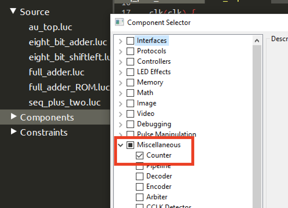
You should see a new script called counter.luc added under Components afterwards. This unit is a synchronous logic unit that receives the following input parameters:
#SIZE(n): defining how many bits is its outputclksignal that synchronizes this unitrstsignal#DIV(i)value (optional): number of bits used as the divisor.
The output of the counter is n bits as defined by the SIZE parameter. Without any DIV, then the counter will produce an output that’s incremented by 1 at every clk cycle.
If i is set to be nonzero, then the counter will produce an n bit output that is incremented by 1 at a slower clock rate – clk is slowed down by $2^i$ times. Therefore, we can use a 1-bit counter as a frequency divider – i.e: produce a clock signal with slower rate.
You don’t have to read the details if you are running low on time. Just know that you can use a
countercomponent with#DIVset to produce a clock signal with slower rate.
Therefore we can declare our counter as follows:
counter slowclock(#SIZE(1),#DIV(26), .clk(clk), .rst(rst));
And use its output as a slower clock for seqplustwo module:
seq_plus_two seqplustwo(.clk(slowclock.value), .rst(rst));
Don’t forget to connect seqplustwo’s output to io_led in the always block.
io_led[0] = seqplustwo.out;
Now you should be able to see that the LEDs are lighted up and they resembles bits of data that’s incremented by 2 periodically. BUT, when you click the reset button, it will not restart the addition back from 0 again! Can you guess why? Don’t worry about it for now. We will tackle this problem in Part 3 of the tutorial.
To enhance your understanding in creating synchronous / sequential logic modules, it is important for you to read this tutorial written by the original author.
Creating a Finite State Machine
Now suppose we want to vary the y input signal to the 8-bit adder in seq_plus_two into the following values in turn every clock cycle (on repeat):
8h02(+2)8h07(+7)8h0C(+12)
So the value out will be the following at each clock cycle:
At t=0: out = 0
*At t=1: out = 2
*At t=2: out = 9
*At t=3: out = 21
*At t=4: out = 23
*At t=5: out = 30
*At t=6: out = 42
*At t=7: out = 44
… *you get the idea.
We can supply these y values using an FSM, having the following simple transition diagram and starting state S0:
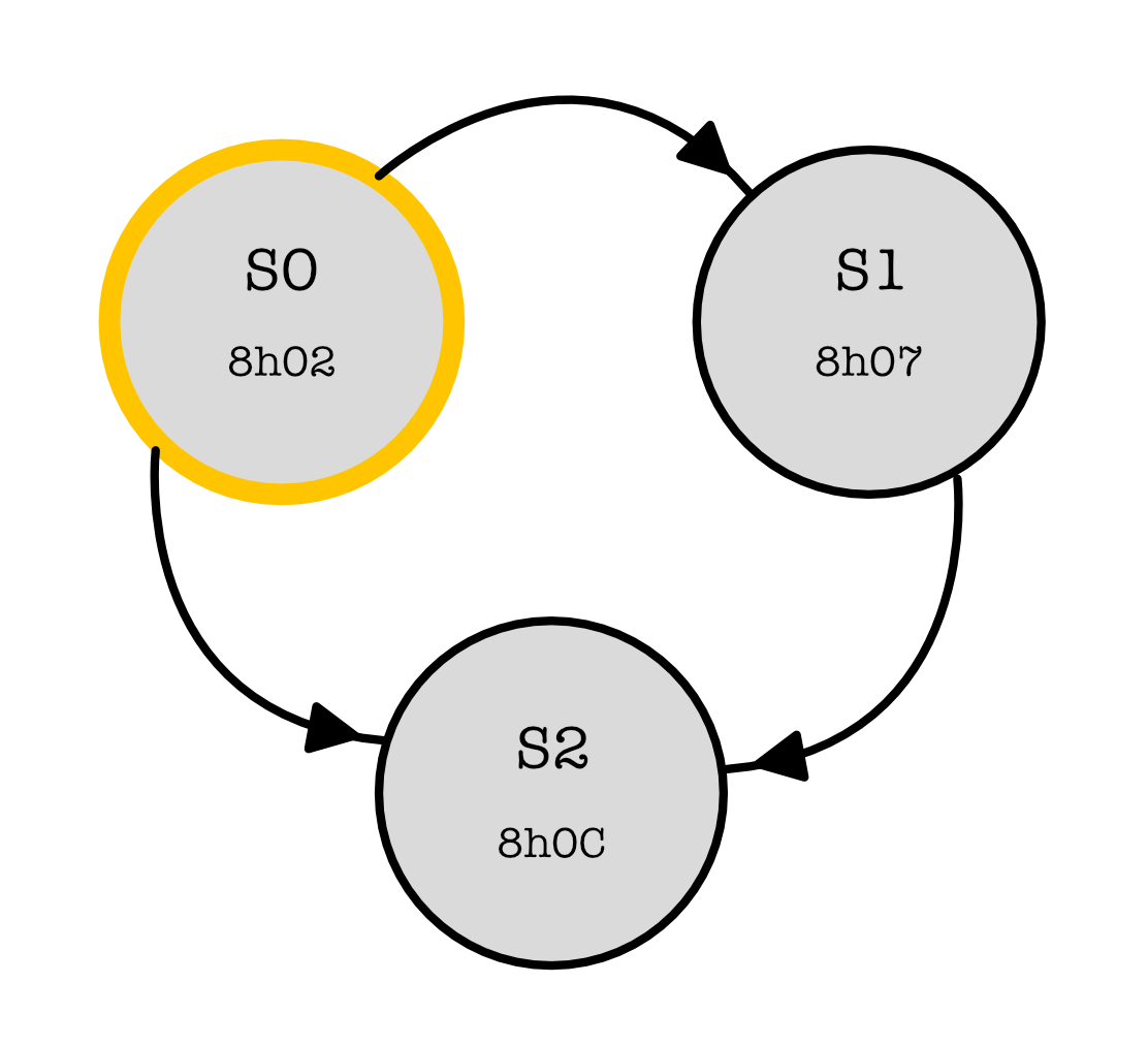
The schematic of the updated sequential logic device (its no longer a plus 2 only now) is:
<img src=”https://dl.dropboxusercontent.com/s/dwc8fl78ibykw22/fsmeg.png?raw=1” width=”60%”
height = “60%”>
We now have that additional FSM unit that controls the value of y instead of just feeding it with the constant 2 like we did previously.
Thankfully Lucid comes with a built-in fsm declaration, so we don’t have to define that FSM by ourselves. fsm is similar to dff except that it is used to store state and not a value.
Think its a little overkill to create an FSM just for this feature of toggling the values of b? Well, there’s many other ways to do this. One possible way is to create a ROM to store the 3 versions of values:
const Y_VALUES = {8h0, 8h0C, 8h07, 8h02}Note:
Y_VALUES[0]is8h02and not8h0.Then, use a 2-bit
dffwhose output value is used as an inputaddressto the ROM. We increment the content of thedffby 1 at each clock cycle, and reset it back to00once it reaches10(because we don’t need11):
dff counter[2](.clk(clk), .rst(rst));
eight_bit_adder adder;

...
// somewhere inside always
adder.y = Y_VALUES[counter.q]
if (counter.q == 2b10){
	counter.d = 2b00;
}
else{
	counter.d = counter.q + 1;
}
...// set other connections for adder
Sounds like so much hassle – technically we can see the
dffas storing a state too, so let’s be a little extra and usefsmmodule instead – because… why not?
Declaring FSM
We can declare our FSM by setting its clk and rst signal, along with the list of states before the always block:
fsm y_controller(.clk(clk), .rst(rst)) = {S0, S1, S2};
Then in the always block, we describe the hardware connections of this module, and the logic for the FSM: to describe what output should be set at each fsm state, and the next state values. The code is pretty descriptive and straightforward.
Create a new module and name it seq_plus_vary.luc to contain this code:
module seq_plus_vary (
	input clk,  // clock
	input rst,  // reset
	output out[8]
  )
{
  dff register_1[8](#INIT(0), .clk(clk), .rst(rst));
  fsm y_controller(.clk(clk), .rst(rst)) = {S0, S1, S2};
  eight_bit_adder adder;

  always {
	adder.y = 8h00;
	adder.x = register_1.q;
	adder.cin = b0;

	case (y_controller.q){
  	y_controller.S0:
      	adder.y = 8h02;
      	y_controller.d = y_controller.S1;
  	y_controller.S1:
      	adder.y = 8h07;
      	y_controller.d = y_controller.S2;
  	y_controller.S2:
      	adder.y = 8h0C;
      	y_controller.d = y_controller.S0;
	}

	adder.cin = b0;
	register_1.d = adder.s;
	out = adder.s;

  }
}
- The line
case (y_controller.q)switches the behaviour of the fsm depending on the current state produced at the output of the fsmy_controller.q. - At each state, we define what the output should be:
- For example when
y_controller.S0case happens, that’s when the current state isS0. It will output8h02as the signal to theyinput port of the adder.
- For example when
- And also define the next state:
- The line
y_controller.d = y_controller.S1;setsS1to be the next state of the fsm. - Therefore in the next positive clock edge, the FSM is at
S1.
- The line
The Tools (Vivado, Alchitry) will intrepret this code and synthesize an appropriate logic circuitry for it on the Au:
- By setting a bunch of logic cells in the Au (LUT) to implement your machine’s logic. Read here for fun facts on how FPGA works.
- Plus some other magic, we don’t really know how the proprietary software does it exactly other than it will utilize some of the 33280 logic cells of the Alchitry Au. So although we have more than enough cells on the Au to emulate reasonable school projects, we can’t really say that it can emulate any hardware (of any size).
To test: As usual, declare seq_plus_vary instance in au_top.luc with the slower clock, and connect its output to some LED on the Io Shield.
You can download seq_plus_vary.luc here.
Summary
In this document, we are given a glimpse on how to create a synchronous / sequential logic circuit. Please also read this tutorial to enhance your understanding. We were also introduced into two new types: dff and fsm. You are recommended to read more about FSM here.
It is important to always remind yourself that the always block contains the hardware description of your device. It is NOT a piece of code that is sequentially executed by a processor like our usual Python and C code (there’s no processor here!). They’re interpreted by Xilinx and Alchitry tools sequentially, but not evaluated sequentially. You should always remind yourself that everything in an always block as being evaluated continuously.
Be careful when using for loops in Lucid. for statements provide a compact way to write something that is otherwise repetitive, but in any case it does NOT work as how for loops in Python or C does.
Refer to Lucid Reference Guide frequently, and do not assume that they work the same way as Python or C. Also, don’t forget to incrementally test your modules:
- Make small modules, define clear input/output terminals
- Test each small module thoroughly: all combinations of input and output must be correct.
- Then make bigger modules
 Computation Structures