
- TOC
50.002 Computation Structures
Information Systems Technology and Design
Singapore University of Technology and Design
Building the \(\beta\) CPU
You can find the lecture video here. You can also click on each header to bring you to the section of the video covering the subtopic.
Overview
In the previous chapter, we were introduced to the \(\beta\) ISA, a CPU blueprint that specifies what instructions the CPU can process, how it interacts with the memory unit, the basic CPU components, instruction formats, and many more.
In this chapter, we will study how each of the 32 \(\beta\) instructions is supposed to work, and how the \(\beta\) CPU (an implementation of the \(\beta\) ISA) is able to compute each and every one of them by reprogramming its datapath without physically changing its hardware.
The key is to have a proper Control Logic unit that is able to decode current instruction’s OPCODE and give out the correct control signals (PCSEL, RA2SEL, ASEL, etc) to reprogram the datapath. The complete truth table of the control logic unit is as shown below,

This unit can be easily implemented using a read only memory.
We will go through the workings of each instruction and understand how the given \(\beta\) datapath is able to execute the instruction properly by producing appropriate control signals as shown above.
Instruction Cycles
Instruction Fetch
The first thing a CPU must do is to compute the address (ia[31:0]) of the instruction to execute next, and then fetch (read) them (id[31:0]) from the Physical Memory Unit (RAM).
Instructions are produced by a compiler and are specific to the CPU’s ISA. The control unit will know what control signals to produce and which signals need to be routed where for each type of instruction.
For example, when you double-click (run) an executable
.exeon Windows, the code for that program is moved from Disk into the Memory Unit (RAM), and the CPU is told what address the first instruction of that program starts at.The CPU always maintains an internal register called the Program Counter (PC) that holds the memory location of the next instruction to be executed.
Once the CPU knows the address of the very first instruction to be executed, it can fetch that first instruction from the Memory Unit and execute it. Figuring out the addresses of the subsequent instructions is easy:
- The first instruction will then tell the CPU what to do next, where is the second instruction, and so on.
- The second instruction will also tell the CPU what to do next, where is the third instruction, and so on.
- This is repeated until the CPU met a
HALT()instruction.
As of now, you always assume that the content of the PC register is always initially zero (32-bit of zeroes), and that the first line of your program instruction is always put at memory address zero (
0x00000000).
Instruction Decoding
When the CPU has an instruction, it needs to figure out (decode) specifically what type of instruction it is. Each instruction will have a certain set of bits called the OPCODE that tells the CPU how to interpret it. In the \(\beta\) ISA, the OPCODE can be found in the 6 most significant bits of the 32-bits instruction. The OPCODE is given as an input to the Control Unit, it will compute the appropriate control signals to program the datapath.
This decoding step depends on how complex the ISA is. An ISA like RISC (e.g: the \(\beta\) ISA) has a smaller number of instructions (a few dozens) while x86 has thousands. The most common family of instructions are:
- Memory Access: anything regarding loading and storing of data between the REGFILE (CPU internal storage) and the Memory Unit. No other computation is performed.
- Arithmetic: anything that requires computation using the ALU, and inputs are taken from the REGFILE.
- Branch instructions: anything pertaining to changing the value of PC Register to load instructions in different Memory Address, (conditional) based on a content of a specific register in the REGFILE.
Detailed Anatomy of the \(\beta\) CPU
The \(\beta\) CPU is comprised of the following standard parts that typically make up a CPU: PC, REGFILE, ALU, and CU.
Program Counter and Physical Memory Unit
The PC is a 32-bit register (i.e: a set of 32 1-bit registers). Its job is to store the address of the current instruction that is executed.
For now, we can safely assume that the initial content of the PC REG is always zero.
The datapath of the components involving the PC and the Physical Memory is shown in the figure below:
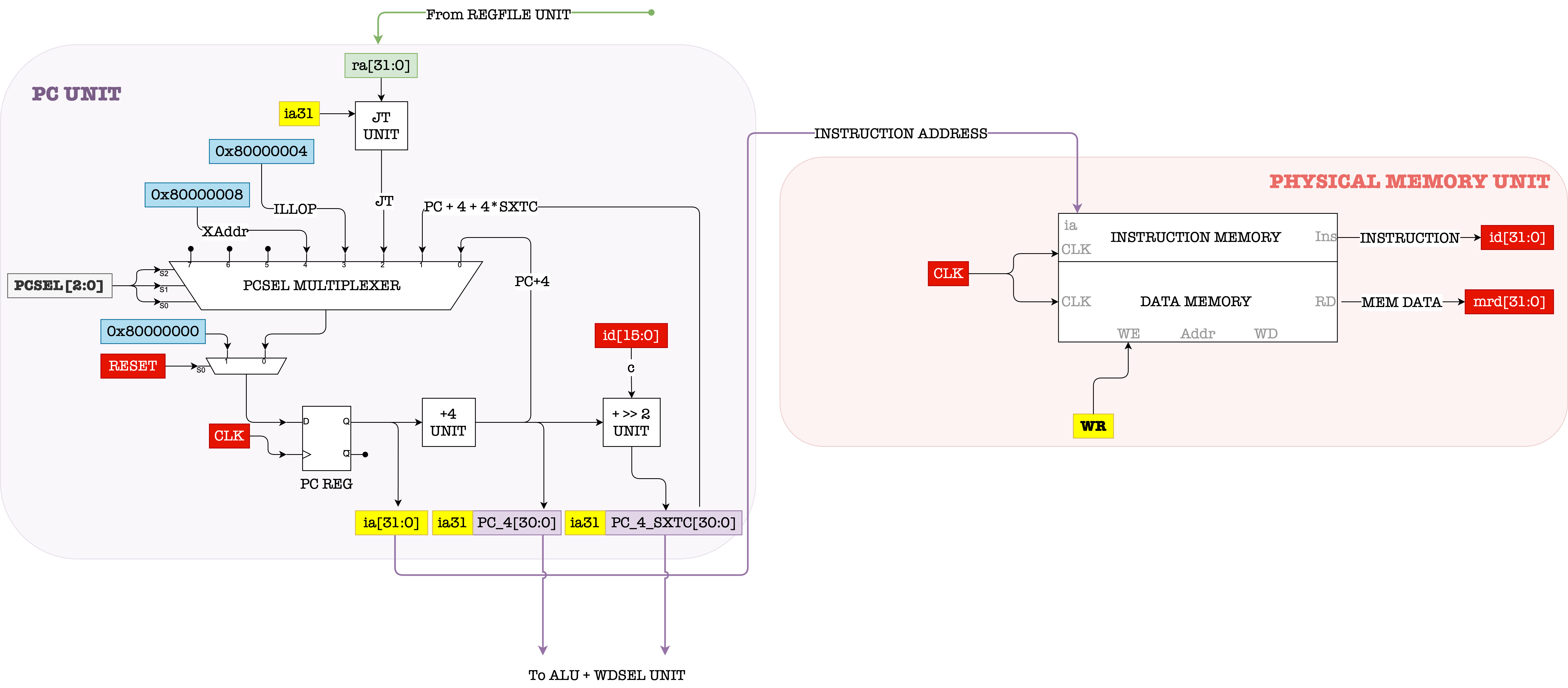
Two important things happened simultaneously at every clock cycle:
-
The output of the PC Register is connected to the
iaport (the input address port) of the Memory Unit (RAM or Physical Memory), hence the Memory Unit will produce the content of that address through theInsport. -
The output of the PC REG will also be added by 4.
- If
PCSEL=0andRESET=0, this value (old PC + 4) will enter the PC REG in the next clock cycle. This will cause the PC to supply the address of the subsequent instruction word in the next clock cycle. - If
PCSEL!=0andRESET=0, then the value in the PC REG will be equivalent to either of the inputs to the PCSEL mux (depending on whatPCSELvalue is).
- If
If RESET=1 then the value of the PC REG in the next cycle will be equivalent to RESET. We will learn what RESET is in the later weeks – but in short, Reset = 0x80000000 all for \(\beta\) instructions. If RESET=1, the value in PC REG will will be set back to 0x0=80000000 in the next clock cycle instead of increased by 4. You will learn in the Virtual Machine chapter on why the MSB of RESET is 1 instead of 0, but for now you can take its purpose as simply resetting the PC REG content back to 0.
The memory unit is neatly segmented into instruction memory and data memory for the sake of learning and simplicity. In reality, this might not always be the case. Your operating system will do the memory management for you and decide where in the physical memory each process should reside and run.
Register Files
The REGFILE in \(\beta\) ISA is the CPU’s internal storage unit that is comprised of 32 sets of 32-bit registers, denoted as \(R_0, R_1, ...., R_{31}\). Each register is addressable in 5 bits. For example: 00000 is the address of \(R_0\), 00001 is the address of \(R_1\), 00010 is the address of \(R_2\), and so on.
Remember, a 32-bit register simply means a set of 32 1-bit registers
The figure below shows the anatomy of \(\beta\) REGFILE component:
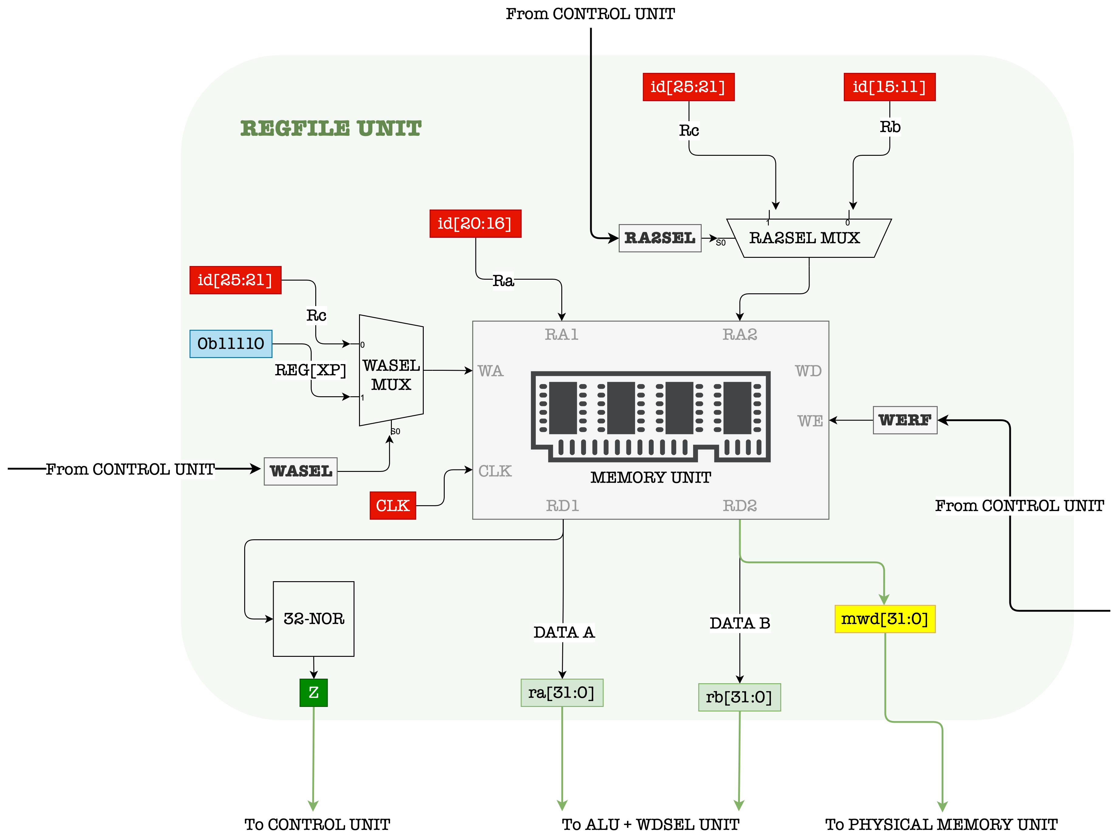
It has two combinational read ports: RD1 and RD2, and one clocked / sequential write port: WD.
We can simultaneously, at the same clock cycle, read the contents of two selected registers, addressable in 5 bits denoted as Ra and Rb, :
- The 5-bit address
Rais supplied through portRA1 - The 5-bit address
Rbis supplied throughRA2
We can also write data supplied at the WD port to any of the registers in the REGFILE:
- In order to write, a valid
1must be supplied at theWEport - The address of the register to write into is determined by the 5-bit input supplied at the
WAport.
The Write Enable Signal
Recall that a register / D Flip-Flop “captures” a NEW input at each CLK rise, and is able to maintain that stable value for the period of the CLK.
However, in practice, we might not want our register to “capture” new input all the time, but only on certain moments. Therefore, there exist a WE signal such that:
- When it’s value is
1, the register “captures” and stores the current input. - Otherwise, the register will ignore the input and will output the last stored value regardless of the CLK edge.
Detailed Anatomy of the REGFILE
To understand how the WE signal works more clearly, we need to dive deeper into the inner circuitry of the REGFILE. The figure below shows a more detailed anatomy of the REGFILE unit.
R31's content is always 0x00000000, regardless of what values are written to it. Therefore it is not a regular register like the other 30 registers in the REGFILE. It is simply giving out 0x00000000 as output when RA1 or RA2 is 11111, which is illustrated as the 0 on the rightmost part of each read muxes.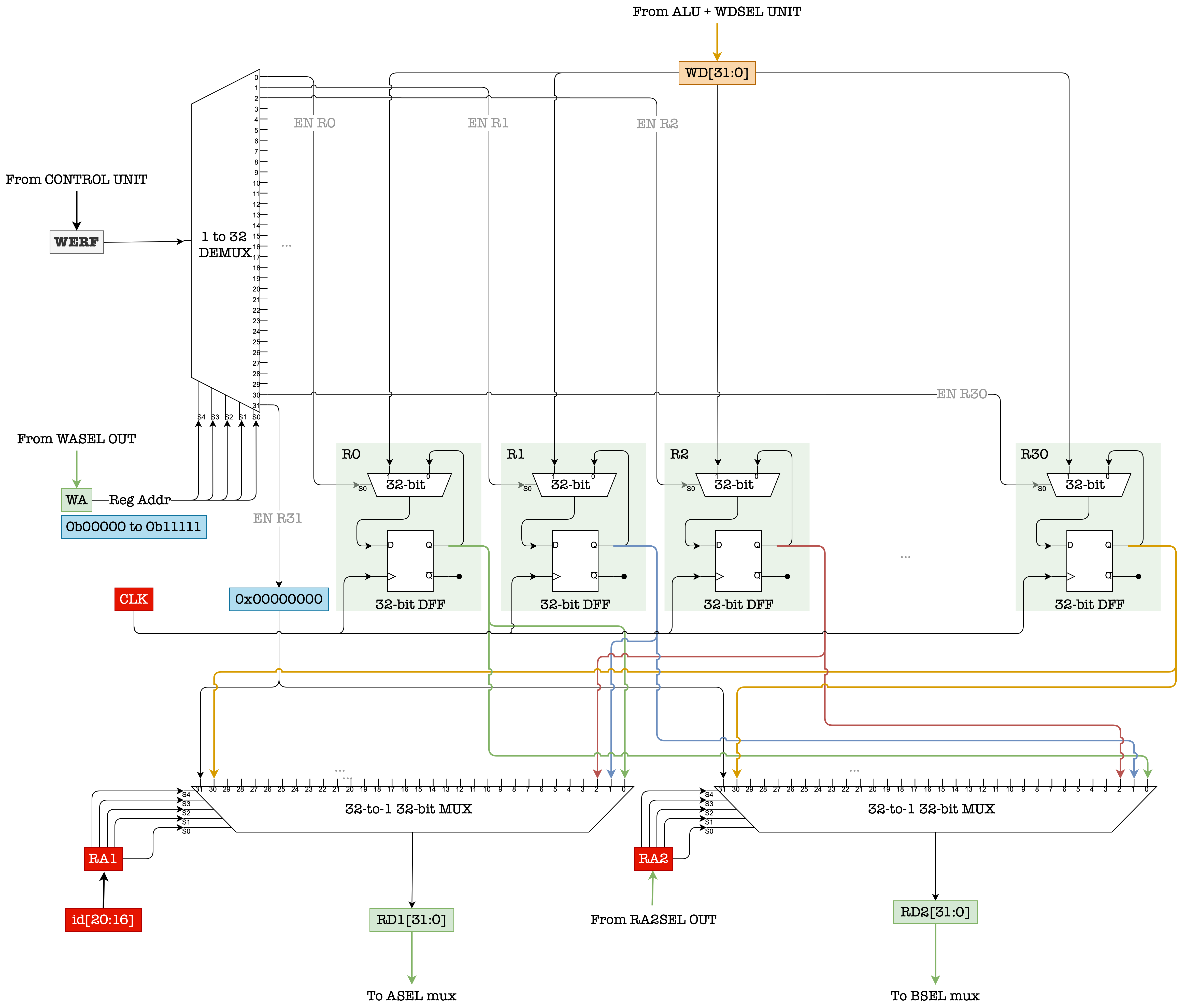
The WE signal is fed into a 1-to-32 demultiplexer unit. The WA signal is the selector of this demux. As a result, only 1 out of the 32 outputs of the demux will follow exactly the value of WE.
The outputs of the demux is used as a selector (EN port) to each of the 2-to-1 32-bit multiplexer connected to each 32-bit register.
Note: although not drawn (to not clutter the figure further), all the registers are synchronized with the same CLK.
The Static and Dynamic Discipline of the REGFILE
As mentioned above, the REGFILE unit has 2 combinational read ports that is made up by the two large 32-to-1 32-bit multiplexers drawn at the bottom of the figure. We can supply two read addresses: RA1 and RA2. They are the selector signals of these two multiplexers. Therefore the time taken to produce valid output (32-bit) data at RD1 and RD2 is at least the \(t_{pd}\) of the multiplexer and \(t_{pd}\) of the DFFs depending on when exactly the addresses become valid.
This unit also have 1 sequential write port. The write data is always supplied at WD. When the EN signal of a target register is a valid 1, we need to wait until the nearest CLK rise edge in order for WD to be reflected at the Q port of that register.
In register transfer language, the content of register with address A is often denoted as : Reg[A]
The timing diagram for read and write is shown below. Please take some time to study them:

Notice how the new data denoted as new Reg[A] supplied at port WD (to be written onto Reg[A]) must fulfill both \(t_S\) and \(t_h\) requirement of the hardware.
Control Logic Unit
The heart of the control logic unit (CU) is a combinational logic device that receives 6-bit OPCODE signal, 1-bit z signal, 1-bit RESET signal, and 1-bit IRQ signal as input. We will discuss about RESET, z and IRQ much later on.
At each CLK cycle, the PC will supply a new 32-bit address to the Memory Unit, and in turn, 32-bit instruction data is produced by the Memory Unit. The first 6 bits of the instruction, called the OPCODE is supplied as an input to the CU.
The CU will then decode the input combination consisted of OPCODE, z, RESET, and IRQ, and produce various control signals as shown in the figure below. In practice, this unit can be made using a ROM.
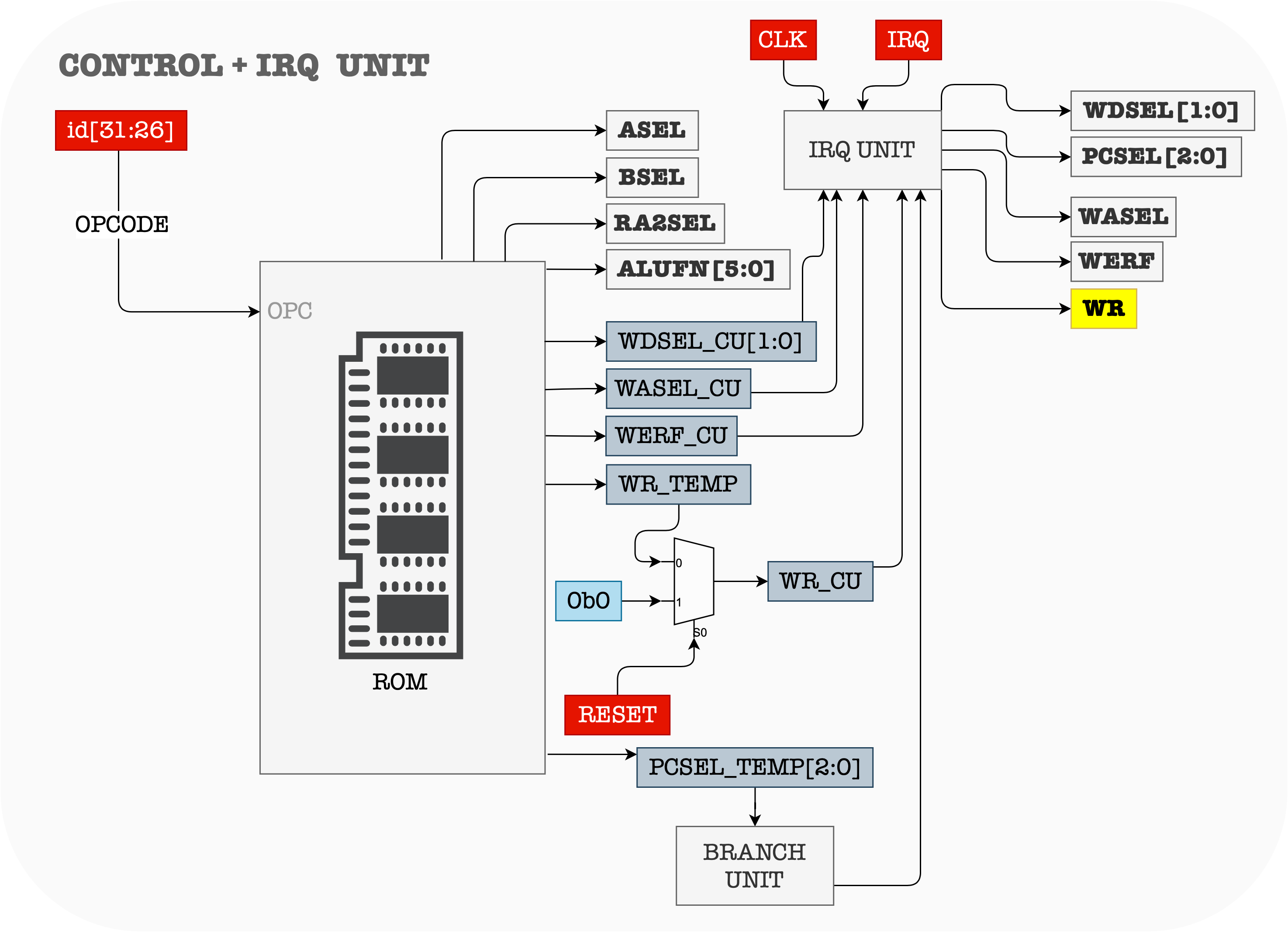
Note that the ALUFN is 6 bits long, PCSEL is 3 bits long, WDSEL is 2 bits long, RA2SEL, BSEL ASEL, WASEL, WR, and WERF (WE to REGFILE) are all 1 bit long. The total number of output bits of the CU is therefore at least 17 bits long
In our Lab however, the output signal of the control unit is 18 bits long. We don’t have to memorise these, as long as we get the main idea.
Notice the presence of the 1-bit register that samples the IRQ signal. This is because. the IRQ signal actually an asynchronous interrupt trigger.
In the later weeks, we will learn that asynchronous interrupts are generated by other hardware devices at arbitrary times with respect to the CPU clock signals. Therefore, we need another sequential logic device to condition/synchronize it such that it doesn’t cause unwanted changes to the Control Unit in the middle of execution (in the middle of a clock cycle). This sampling device that receives the external
IRQsignal allows the CPU to sample the input IRQ signal during the beginning of each instruction cycle, and will respond to the trigger only if the signalIRQis asserted when sampling occurs.
In the Lab however, we also simplify this part. We simply assume that the IRQ signal given by the test file is guaranteed to be stable for the entire CPU clock cycle, and already fulfils the \(t_S\) and \(t_H\) requirements of the CPU clock cycle.
For simplicity, we no longer display this register unit in the diagrams to explain the datapaths below. The presence of the CLK signal there is written to remind you that the CPU should be able to sample the asynchronous IRQ signal for each clock cycle. However, the heart of the Control Unit itself is combinational logic device (e.g: ROM) and not a sequential one.
Beta Datapaths
The \(\beta\) datapath can be reprogrammed by setting the appropriate control signals depending on the current instruction’s OPCODE. In general, we can separate the instructions into four categories, and explain the datapath for each:
- The
OPdatapath (Type 1) - The
OPCdatapath (Type 2) - Memory access datapath (Type 2)
- Control transfer datapath (Type 2)
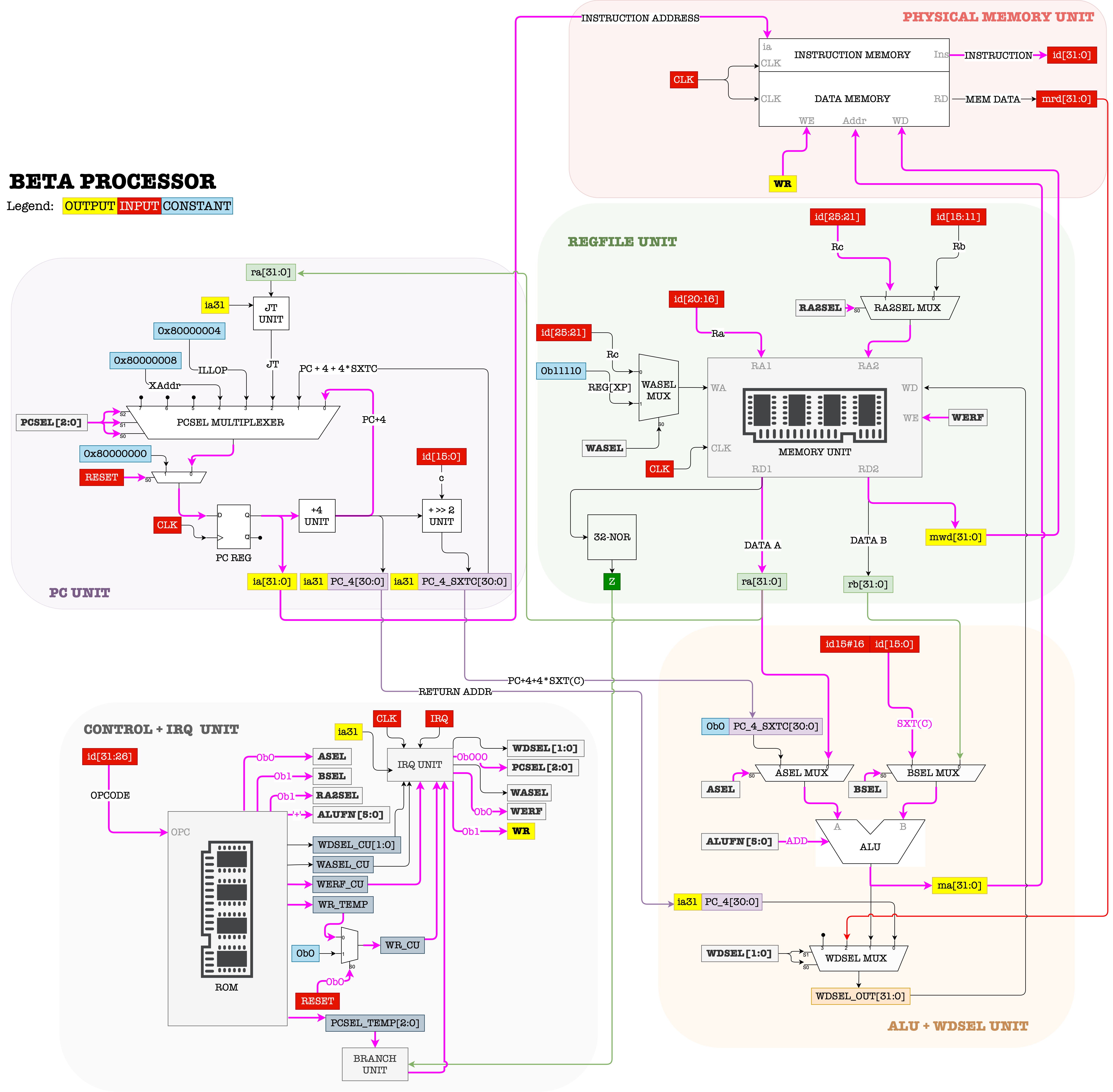
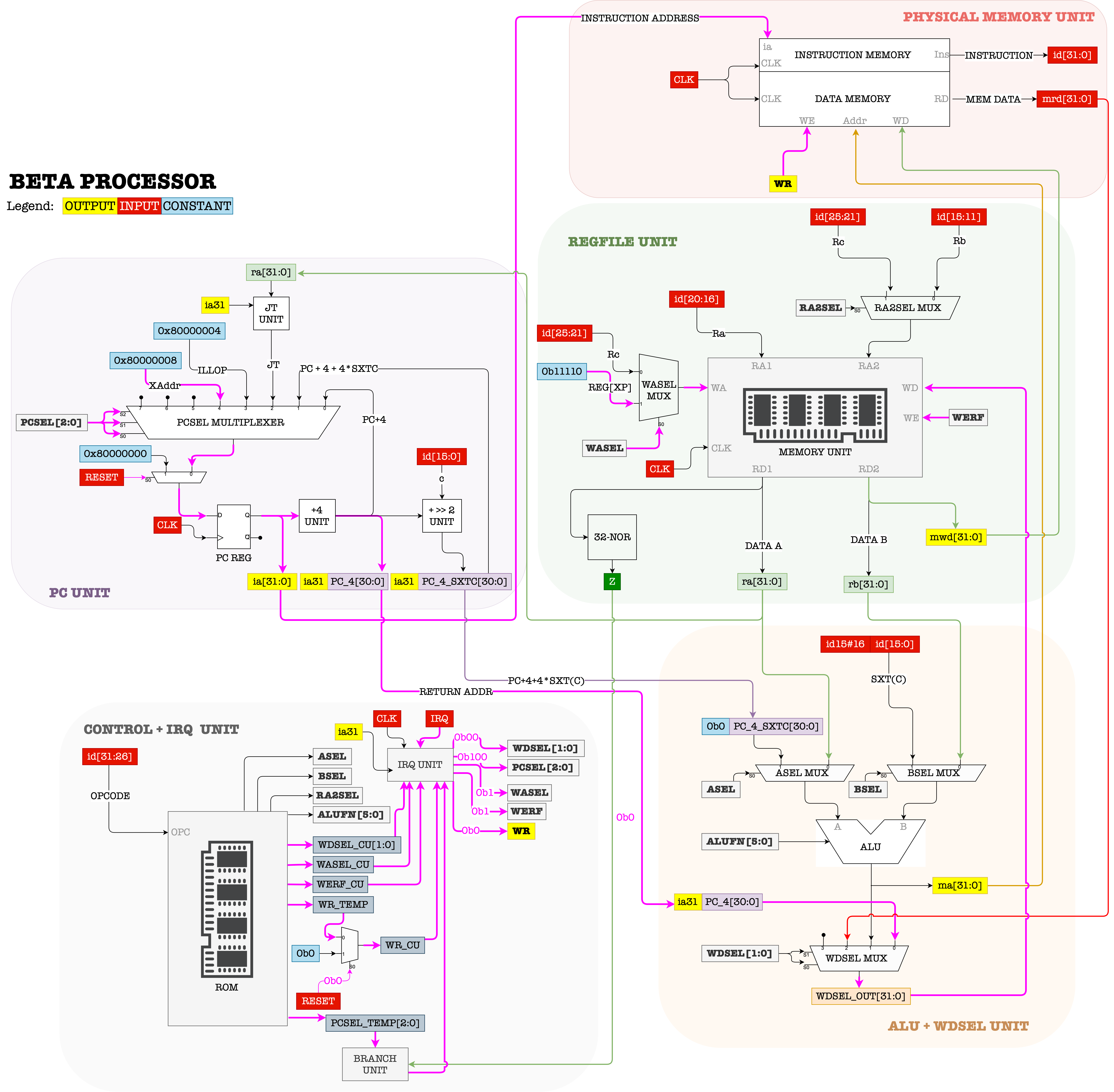
OP datapath
This datapath involves:
- Any logical computations using the ALU, and
- The inputs to the
AandBport of the ALU is taken from the contents of any two registersReg[Ra]andReg[Rb]from the REGFILE. - The result is stored as a content of
Reg[Rc]
The instructions that fall under OP category are: ADD, SUB, MUL, DIV, AND, OR, XOR, CMPEQ, CMPLT, CMPLE, SHL, SHR, and SRA. Its general format is:

The register transfer language for this instruction is:
PC \(\leftarrow\) PC+4
Reg[Rc] \(\leftarrow\) Reg[Ra] (OP) Reg[Rb]
- The corresponding assembly instruction format runnable in BSIM is
OP(Ra, Rb, Rc)
Important: Read the \(\beta\) documentation and fully study the functionalities of each instruction.
The figure below shows the datapath for all OP instructions:
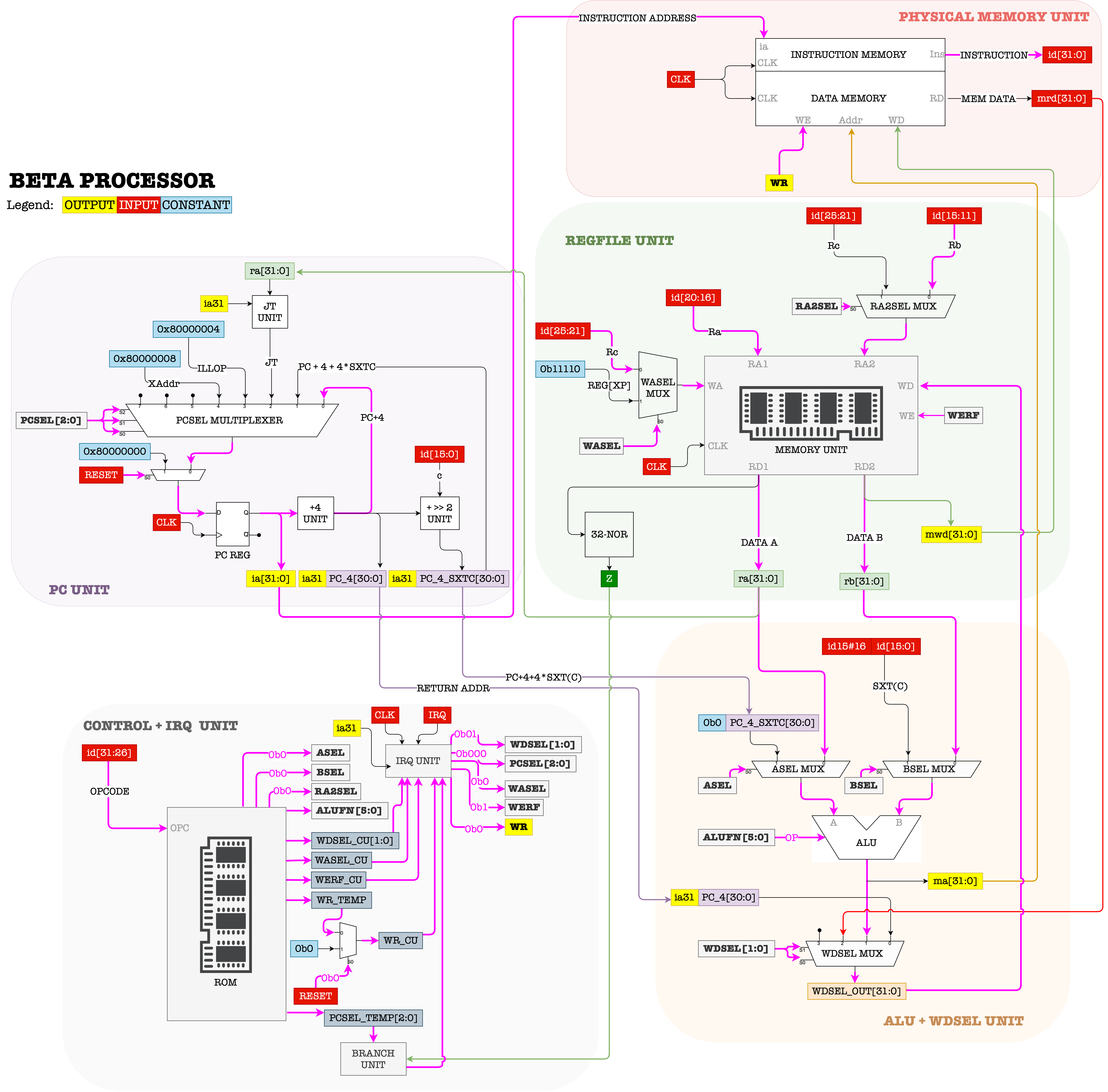
The highlighted lines in pink show how the signals should flow in order for the \(\beta\) to support OP instructions.
The control signals therefore must be set to:
-
ALUFN = F(OP)the
ALUFNsignal for the corresponding operationOP, for example, ifOPCODE = SUBthenALUFN = 010001, and so on. -
WERF = 1 -
BSEL = 0 -
WDSEL = 01 -
WR = 0 -
RA2SEL = 0 -
PCSEL = 000 -
ASEL = 0 -
WASEL = 0
Take some time to understand why the value of these control signals must be set this way to support the
OPinstructions.
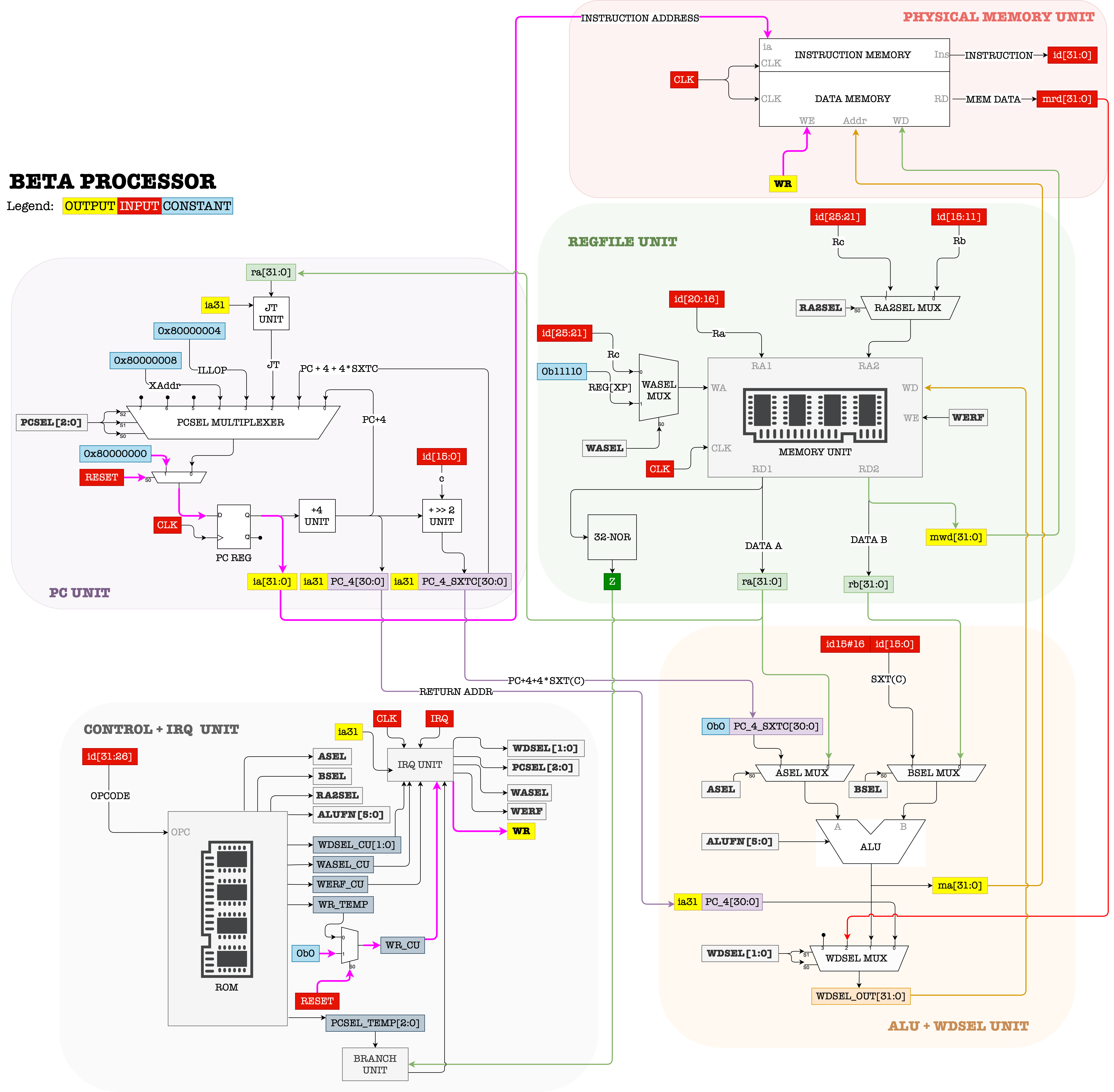
OPC datapath
The OPC (Type 2 instruction) datapath is similar to the OP datapath, except that input to the B port of the ALU must comes from c = I[16:0].
There is no Rb field in Type 2 instruction.
The instructions that fall under OPC category are: ADDC, SUBC, MULC, DIVC, ANDC, ORC, XORC, CMPEQC, CMPLTC, CMPLEC, SHLC, SHRC, and SRAC. It’s general format is:

The register transfer language for this instruction is:
PC \(\leftarrow\) PC+4
Reg[Rc] \(\leftarrow\) Reg[Ra] (OP) SEXT(C)
Again, don’t forget to read \(\beta\) documentation to understand each functionalities.
- The corresponding assembly instruction format runnable in BSIM is
OPC(Ra, c, Rc)
The figure below shows the datapath for all OPC instructions:
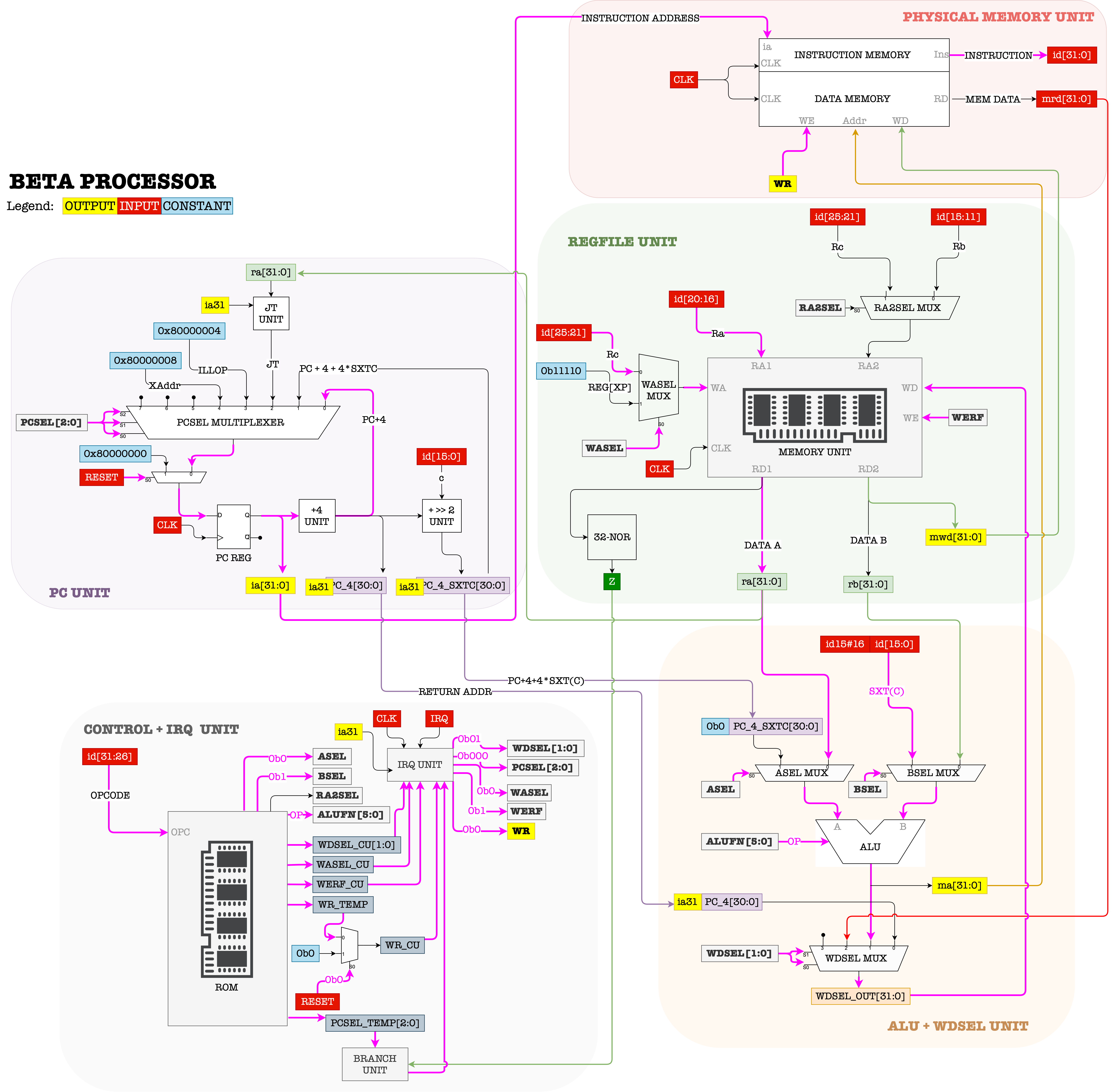
The control signals for OPC instructions are almost identical to OP operations, except that we need to have BSEL = 1.
Sample Code
Try it yourself by running this code step by step on BSIM and observe the datapath to familiarize yourself with how OP and OPC datapath works.
- At each timestep, be aware of the value of PC and all Registers.
- Familiarise yourself with how to translate from the assembly language to the 32-bit machine language
1
2
3
4
5
6
7
8
9
10
.include beta.uasm

ADDC(R31, 5, R0)
SUBC(R31, 3, R1)
MUL(R0, R1, R2)
CMPEQ(R1, R1, R4)
CMPLT(R0, R1, R4)
SHL(R1, R1, R5)
SRAC(R5, 4, R5)
SHRC(R1, 4, R6)
Memory Access Datapath
There are three instructions that involve access to the Memory Unit: LD, LDR and ST. All of them are Type 2 instructions.
LD Datapath
The general format of the LD instruction is:

The register transfer language for this instruction is:
PC \(\leftarrow\) PC+4
EA \(\leftarrow\) Reg[Ra] + SEXT(C)
Reg[Rc] \(\leftarrow\) Mem[EA]
-
The LD instruction allows the CPU to load one word (32-bit) of data from the Memory Unit and store it to
Rc - The effective address (
EA) of the data is computed using the content ofRa(32-bit) added withc(sign extended to be 32-bit). - The corresponding assembly instruction format runnable in BSIM is
LD(Ra, c, Rc)
The figure below shows the datapath for LD:
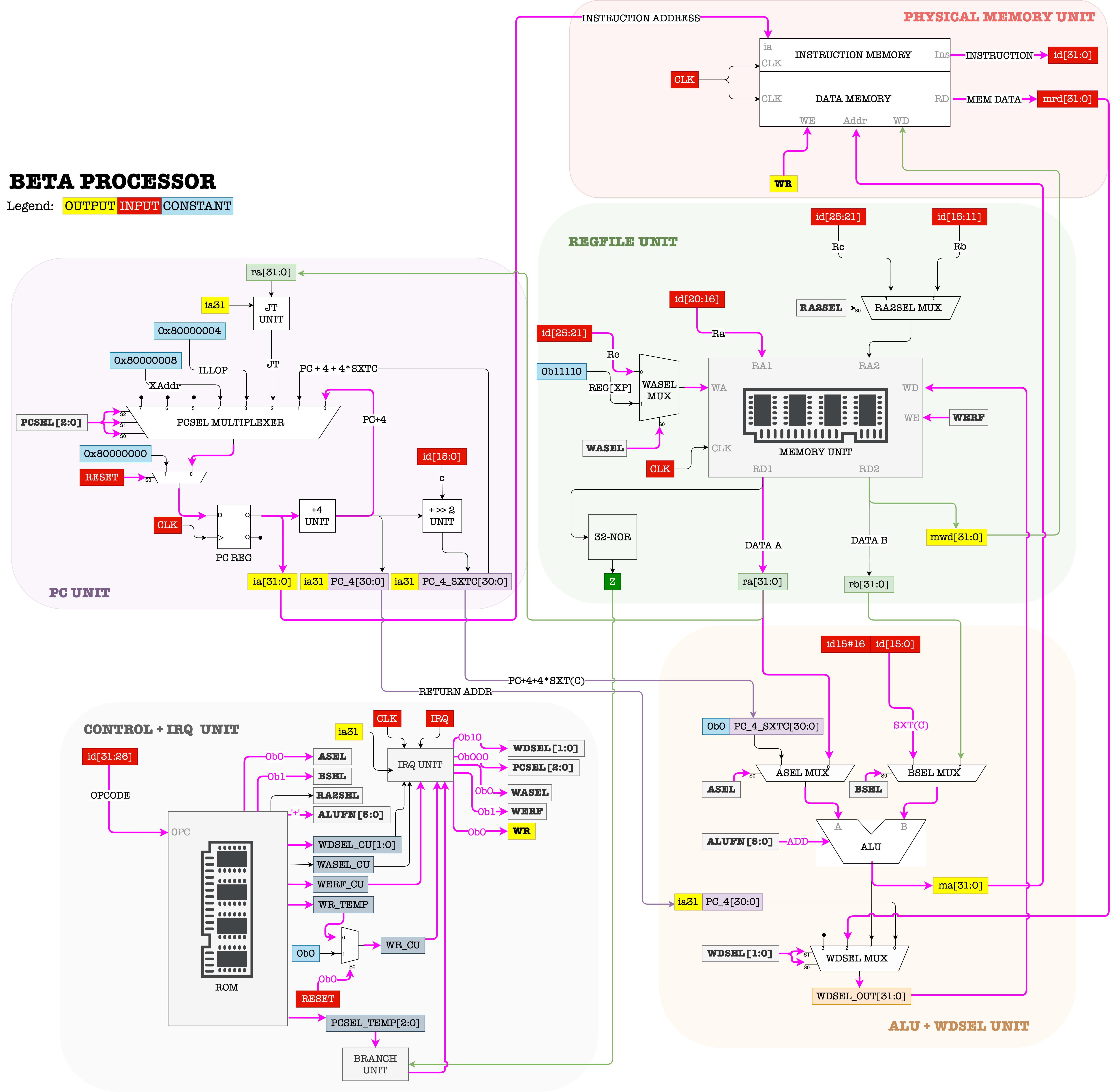
The control signals therefore must be set to:
-
ALUFN = ADD (000000) -
WERF = 1 -
BSEL = 1 -
WDSEL = 10 -
WR = 0 -
RA2SEL = -- -
PCSEL = 000 -
ASEL = 0 -
WASEL = 0
LDR datapath
The LDR instruction is similar to the LD instruction, except in the method of computing the EA of the data loaded.
The general format of the LDR instruction is:

The register transfer language for this instruction is:
PC \(\leftarrow\) PC+4
EA \(\leftarrow\) PC+4*SEXT(C)
Reg[Rc] \(\leftarrow\) Mem[EA]
- The
LDRinstruction computesEArelative to the current address pointed byPC. - The corresponding assembly instruction format runnable in BSIM is
LDR(label, Rc), wherecis auto computed as(address_of_label - address_of_current_ins)/4-1
The figure below shows the datapath for LDR:
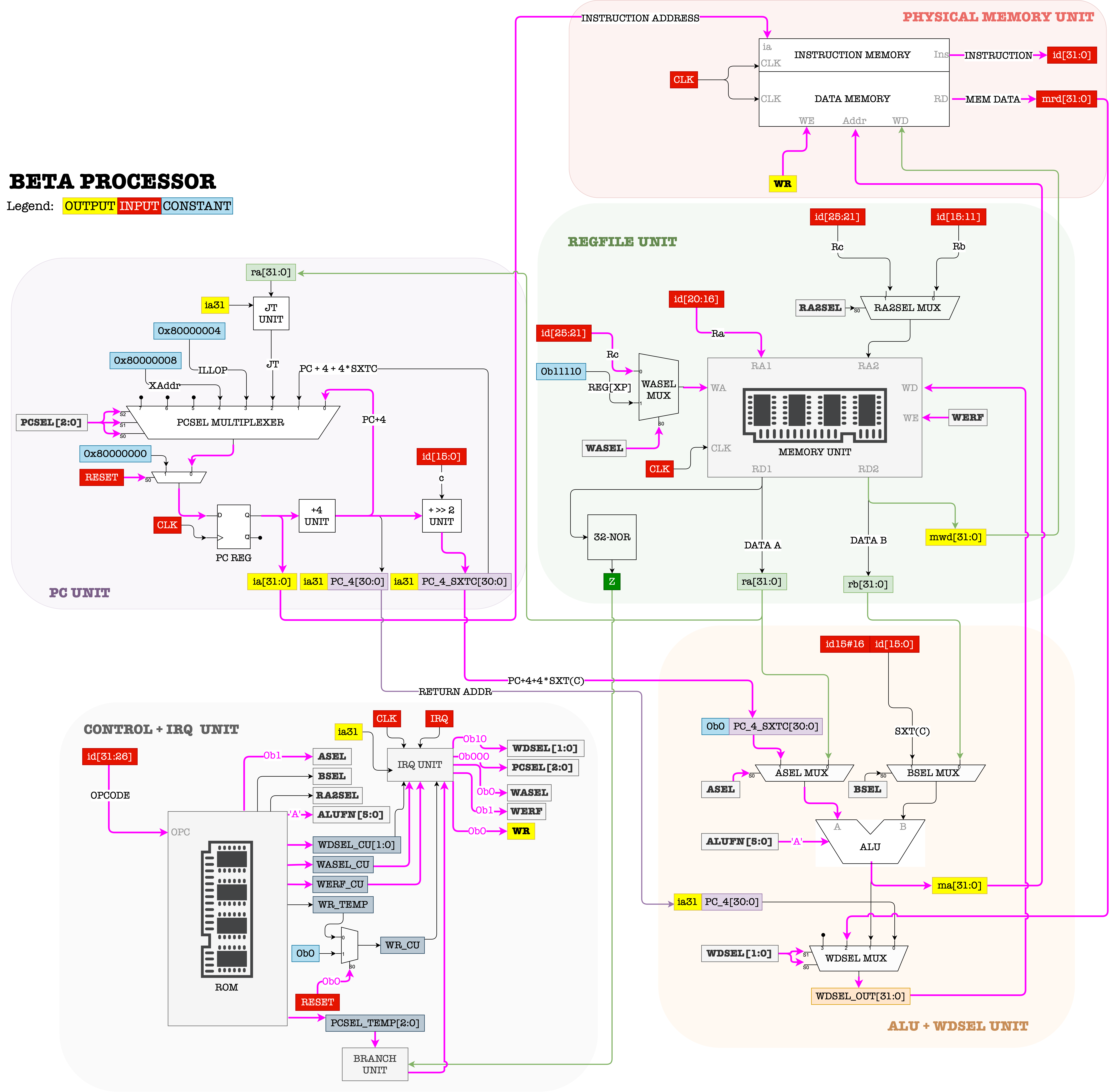
The control signals therefore must be set to:
-
ALUFN = 'A' (011010)The ALU is simply required to be transparent, i.e: “pass” the input at the
Aport through to its output port. -
WERF = 1 -
BSEL = -- -
WDSEL = 10 -
WR = 0 -
RA2SEL = -- -
PCSEL = 000 -
ASEL = 1 -
WASEL = 0
ST datapath
The ST instruction does the opposite to what the LD instruction does. It allows the CPU to store contents from one of its REGFILE registers to the Memory Unit.
Note that the instruction
STandLD/LDRallows the CPU to have access to an expandable memory unit without changing its datapath, although the CPU itself has a limited amount of internal storage in the REGFILE.
The general format of the ST instruction is:

The register transfer language for this instruction is:
PC\(\leftarrow\)PC+4EA\(\leftarrow\)Reg[Ra]+SEXT(c)-
Mem[EA]\(\leftarrow\)Reg[Rc] -
The ST instruction stores data present in
Rcto the Memory Unit. - Similar to how
EAis computed forLD, the effective address (EA) of where the data is supposed to be stored is computed using the content ofRa(32-bit) added withc(sign extended to be 32-bit). - The corresponding assembly instruction format runnable in BSIM is
ST(Rc, c, Ra), notice the swappedRcandRaposition.
The figure below shows the datapath for ST:
The control signals therefore must be set to:
-
ALUFN = 'ADD' (000000) -
WERF = 0 -
BSEL = 1 -
WDSEL = -- -
WR = 1 -
RA2SEL = 1 -
PCSEL = 000 -
ASEL = 0 -
WASEL = --
Sample Code
Try it yourself by running this code step by step on BSIM and observe the datapath to familiarize yourself with how OP and OPC datapath works.
- At each timestep, be aware of the value of PC and all Registers.
- Be aware on the value stored at certain memory locations
- Familiarise yourself with how to translate from the assembly language to the 32-bit machine language using labels and literals
1
2
3
4
5
6
7
8
9
10
11
12
13
14
15
16
17
18
.include beta.uasm

LD(R31, x, R0)
LD(R31, x + 4, R1)
LD(R31, x + 8, R2)
LD(R31, x + 12, R3)
LDR(x, R4)
LDR(x+8, R5)
MUL(R0, R3, R0)
ADD(R1, R1, R1)
ADDC(R31, 12, R6)
ST(R0, x)
ST(R1, x, R6)

x : LONG(15) | this is an array
	LONG(7)
	LONG(9)
	LONG(-1)
Control Transfer Datapath
There are three instructions that involves transfer-of-control (i.e: branching, or jumping), that is to change the value of PC so that we can execute instruction from other EA in the Memory Unit instead of going to the next line. These instructions are BEQ, BNE, and JMP.
We will not use the ALU at all when transferring control.
So far, we have only seen
PCto be advanced by 4:PC\(\leftarrow\)PC+4. With instructions involving transfer-of-control or , we are going to setPCa little bit differently.
BEQ datapath
This instruction allows the PC to branch to a particular EA if the content of Ra is zero. It is commonly used when checking for condition prior to branching, e.g: if x==0, else.
The general format of the BEQ instruction is:

The register transfer language for this instruction is:
PC \(\leftarrow\) PC+4
Reg[Rc] \(\leftarrow\) PC
EA \(\leftarrow\) PC + 4*SEXT(C)
if (Reg[Ra] == 0) then PC \(\leftarrow\) EA
- The address of the instruction following the
BEQinstruction is written toRc. - If the contents of
Raare zero, thePCis loaded with the target addressEA; - Otherwise, execution continues with the next sequential instruction.
- The checking of the content of
Rais not done through ALU, but rather through the 32-bit NOR gate that producesZ(1-bit), The value ofZis fed to the CONTROL UNIT to determine whether PCSEL should be001or000depending on the value ofZ. - The corresponding assembly instruction format runnable in BSIM is
BEQ(Ra, label, Rc)wherecis auto computed as(address_of_label - address_of_current_ins)/4-1
The figure below shows the datapath for the BEQ:
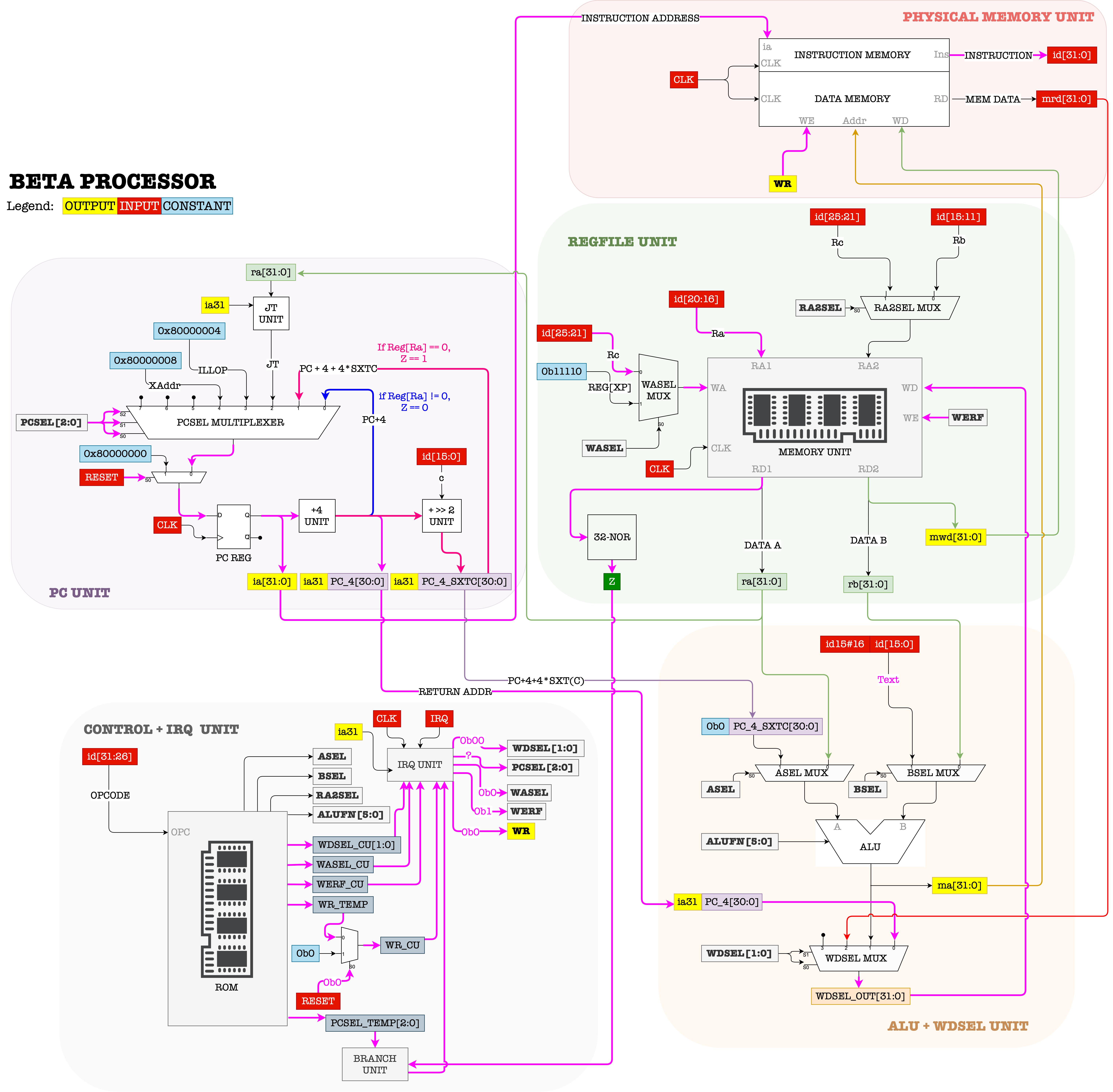
The control signals therefore must be set to:
-
ALUFN = --We aren’t using the ALU at all when transferring control.
-
WERF = 1 -
BSEL = -- -
WDSEL = 00 -
WR = 0 -
RA2SEL = -- -
PCSEL = Z ? 001 : 000 -
ASEL = -- -
WASEL = 0
BNE datapath
BNE is similar to BEQ, but branches PC in the opposite way, i.e: when Ra != 0. It also utilizes the output Z.
The general format of the BNE instruction is:

The register transfer language for this instruction is:
PC \(\leftarrow\) PC+4
Reg[Rc] \(\leftarrow\) PC
EA \(\leftarrow\) PC + 4*SEXT(C)
if (Reg[Ra] != 0) then PC \(\leftarrow\) EA
- The corresponding assembly instruction format runnable in BSIM is
BNE(Ra, label, Rc)wherecis auto computed as(address_of_label - address_of_current_ins)/4-1
The figure below shows the datapath for the BNE:
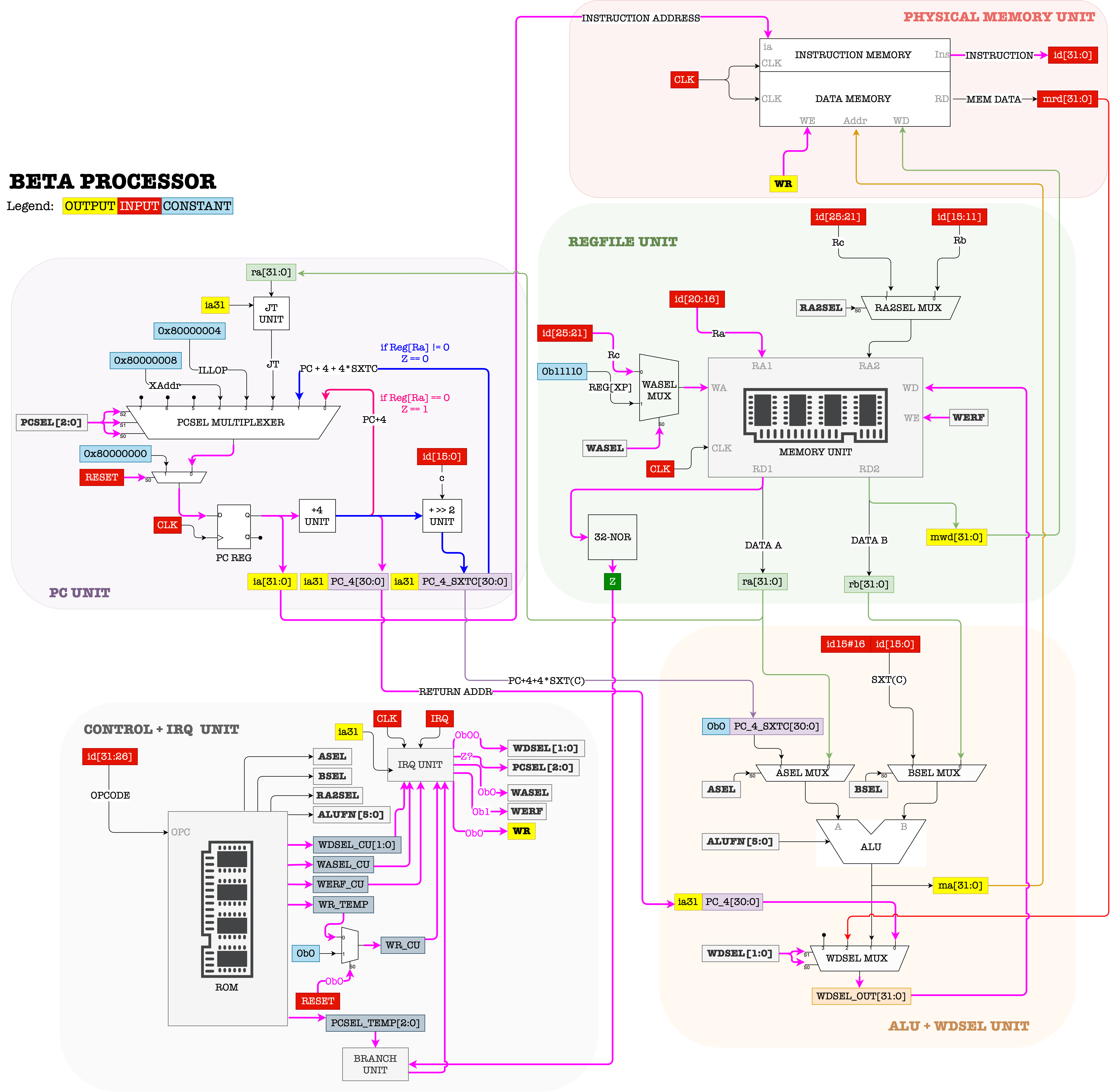
The control signals therefore must be set to:
-
ALUFN = --We aren’t using the ALU at all when transferring control.
-
WERF = 1 -
BSEL = -- -
WDSEL = 00 -
WR = 0 -
RA2SEL = -- -
PCSEL = Z ? 000 : 001 -
ASEL = -- -
WASEL = 0
JMP Datapath
JMP also allows the CPU to change its PC value, but without any condition (jump).
The general format of the JMP instruction is:

The register transfer language for this instruction is:
PC \(\leftarrow\) PC+4
Reg[Rc] \(\leftarrow\) PC
EA \(\leftarrow\) Reg[Ra] & 0xFFFFFFFC (masked)
PC\(\leftarrow\) EA
- The address of the instruction following the
JMPinstruction is written toRc, thenPCis loaded with the contents ofRa. - The low two bits of
Raare masked to ensure that the target address is aligned on a 4-byte boundary. - The corresponding assembly instruction format runnable in BSIM is
JMP(Ra, Rc).
The figure below shows the datapath for the JMP:
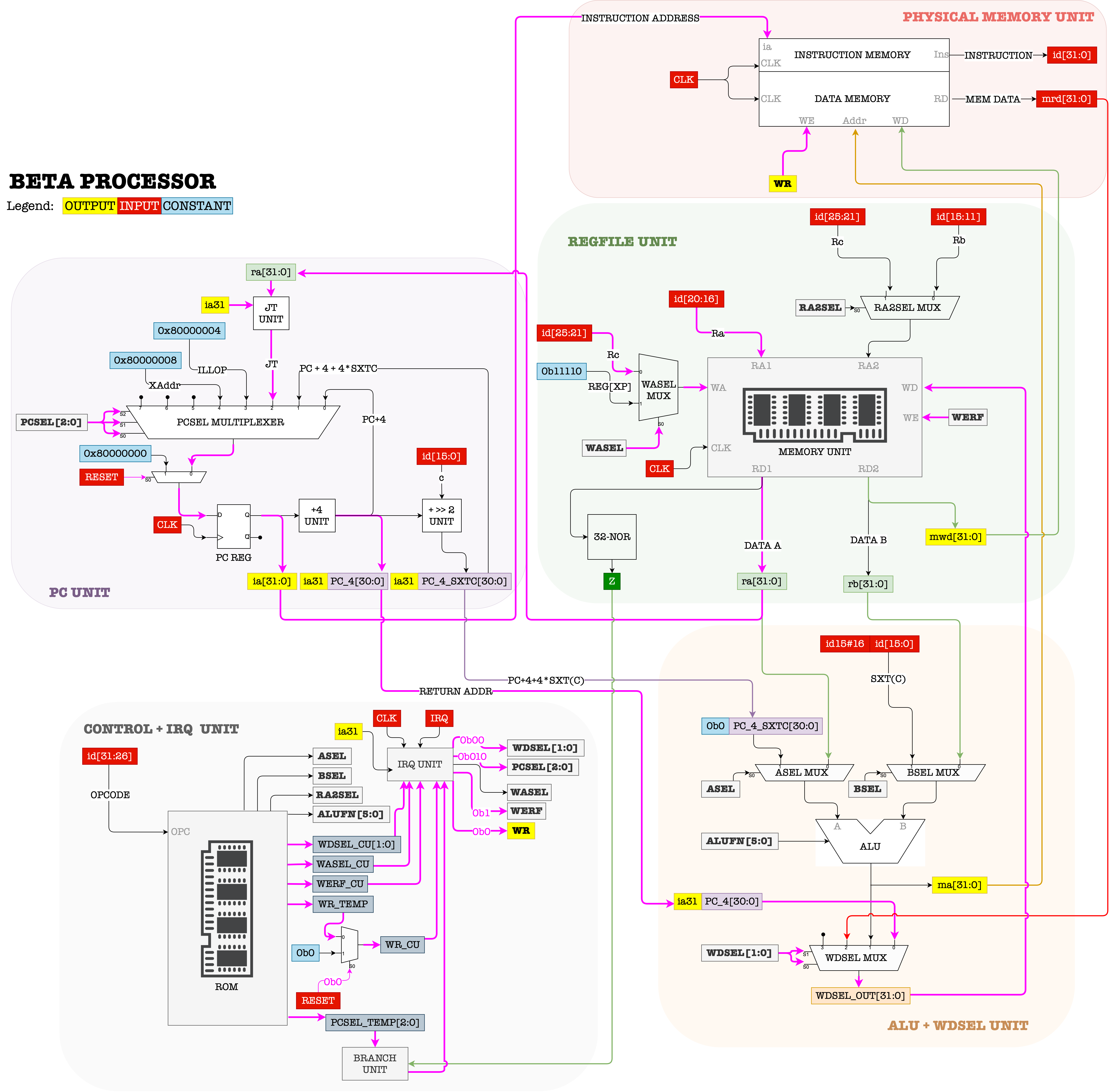
The control signals therefore must be set to:
-
ALUFN = --We aren’t using the ALU at all when transferring control.
-
WERF = 1 -
BSEL = -- -
WDSEL = 00 -
WR = 0 -
RA2SEL = -- -
PCSEL = 010 -
ASEL = -- -
WASEL = 0
Sample Code
Try it yourself by running this code step by step on BSIM and observe the datapath to familiarize yourself with how OP and OPC datapath works.
- At each timestep, be aware of the value of PC and all Registers.
- Know where is the address of each instruction when loaded to memory
- Note how to translate from
labeltoliteralwhen crafting the 32-bit machine language forBEQ/BNEinstructions.
1
2
3
4
5
6
7
8
9
10
.include beta.uasm

ADDC(R31, 3, R0)

begin_check: CMPEQ(R31, R0, R1)
BNE(R1, is_zero, R10)
SUBC(R0, 1, R0)
BEQ(R31, begin_check, R10)

is_zero: JMP(R31)
Exception Handling
Exceptions as the name suggests, is an event generated by the CPU when an error occurs.
\(\beta\) exceptions come in three flavors: traps, faults, and interrupts.
-
Traps (intentional) and faults (unintentional) are both the direct outcome of an instruction and are distinguished by the programmer’s intentions.
- These happens for example when we supply an illegal
OPCODE, i.e: it does not correspond to any of the instructions defined in the ISA.
- These happens for example when we supply an illegal
-
Interrupts are asynchronous with respect to the instruction stream, and are usually caused by external events, for example from I/O devices, or network devices. This would require us to “pause” the execution of the current program and handle the interrupt.
- At the beginning of each cycle, the CPU will always check whether
IRQ == 1. - If
IRQ != 1, the CPU will continue with normal execution. - If
IRQ == 1, the CPU will pause the current execution and handle the interrupt request first (and eventually resume back the paused execution after the interrupt handling is done).
- At the beginning of each cycle, the CPU will always check whether
The datapath that handles trap/fault (due to Illegal OPCODE) is as follows:

The datapath that handles interrupt (due to asynchronous IRQ signal) is as follows:
There’s only one difference between the two: the datapath at the PCSEL mux.
The PCSEL multiplexer’s fourth and fifth input are called ILLOP and XAdr. These refers to the address of the instruction branching to the interrupt handling code, in the events that trap, fault, or interrupt occurs. In \(\beta\) ISA,
ILLOPis set at0x80000004XAdris set at0x80000008
The control signals in the events of these exceptions therefore must be set to:
-
ALUFN = --We aren’t using the ALU at all when transferring control.
-
WERF = 1 -
BSEL = -- -
WDSEL = 00 -
WR = 0 -
RA2SEL = -- -
PCSEL:Illegal_Opcode ? 011 : 000IRQ ? 100 : 000
-
ASEL = -- -
WASEL = 1
Note that since WASEL = 1 and WDSEL = 00 and WERF = 1, then PC+4 (supposed next instruction’s address) is stored at Reg[XP] (register 30, or 11110 in binary) so that we may resume the execution once the exception has been handled.
CPU Reset
Finally, the \(\beta\) processor accept external RESET signal that can reset the value of the PC. The signal RESET must be 1 for several clock cycles in order to ensure that the values affected by RESET propagates throughout the entire circuit. During the period where RESET = 1, we need to make sure that WR is 0 so that we do not accidentally overwrite the content of the physical memory.
CPU Benchmarking
We always want a CPU that has a high performance (most instruction per second) at a low cost. Unfortunately there will always be a tradeoff between the two. We can benchmark the quality of a CPU by computing its \(MIPS\) (million instruction per second),
\[MIPS = \frac{Clock Rate }{CPI}\]where \(CPI\) means “Clocks per Instruction”.
Although it is common to judge a CPU’s performance from its clock rate (cycles per second, typically ranging between 2-4 GHz per core for modern computers), we also need to consider another metric called the \(CPI\), that is the average clock cycles used to execute a single instruction.
In \(\beta\) ISA, each instruction requires only 1 clock cycle to complete (atomic execution). It is possible for other ISA to take more than 1 clock cycle on average to complete an instruction.
Typically, one will choose a particular program (with fixed number of instructions) for benchmarking purposes, and the same benchmark program is run on different CPUs with potentially different Clock Rate and \(CPI\).
The higher the \(MIPS\), the faster it takes to run the benchmark program. Therefore we can say that a CPU with the highest \(MIPS\) has the best performance.
Summary
You may want to watch the post lecture videos here:
In this notes we have covered extensively how to create the \(\beta\) CPU datapath given its ISA (blueprint). We can run some instructions written in machine language (0s and 1s), but obviously it is not yet user friendly at all. Not to mention that this CPU alone does not support reusable instructions (we know them as functions). The next lecture introduces us to assemblers and compilers, which are softwares created to help us utilise the \(\beta\) CPU better so that we are focused on programming it and spending more time thinking about designing our program, and less time writing the program.